ISSN (Print) : 2320 – 3765 ISSN (Online): 2278 – 8875
I
nternational
J
ournal of
A
dvanced
R
esearch in
E
lectrical,
E
lectronics and
I
nstrumentation
E
ngineering
(An ISO 3297: 2007 Certified Organization)
Vol. 3, Issue 11, November 2014
10.15662/ijareeie.2014.0311079
Design of Low Power Non Volatile Magnetic
Flip-Flop or Memories Based on Lector
Technique
D.shilpa1, S.Senthurpriya2
PG Scholar, Department of ECE,Muthayammal Engineering College, Namakkal, India1
Assistant Professor, Department of ECE,Muthayammal Engineering College, Namakkal, India2
ABSTRACT: Power has becoming a burning issue in modern VLSI design. Non volatile memories like MRAM, FeRAM , ReRAM etc can save power by allowing the system power off in standby state. MRAM can be built up by using Magnetic Flip-flop like portable computer, Floppy disk, CD's etc. Comparing to the conventional Flip-flop STT-MRAM can save the power and retain the data by using 22 nm technology .Advanced computing systems suffer from high static power due to rapidly rising leakage currents in deep sub-micron MOS technologies. In this paper performed electrical simulations to validate its functional behaviors and evaluate its performance by using spice model of STT-MRAM. Some mechanisms like checkpointing/power gating has been undergone in this NVM(non-volatile memories). There are numerous methods proposed to control leakage power dissipation. LECTOR is one of the techniques used for leakage reduction without affecting the dynamic power. The proposed design requires less design effort and offers greater power reduction and smaller area cost than the previous method. in leakage power reduction when compared to all other existing leakage reduction techniques. Using this LECTOR technique, power efficiency becomes better. This paper presents the analysis for leakage current in Static RAM implementing LECTOR technique
KEYWORDS: Checkpointing,flip-flop, STT-MRAM, non-volatile, LECTOR
I. INTRODUCTION
Non-volatile memories (NVM) are to be integrated in Flip-Flops or memories to allow system power-off in standby state and save power. STT-MRAM has high speed, low power, and infinite endurance. Power consumption consists of dynamic and static power, the main function of dynamic power is to charging and discharging of load capacitance at an average frequency over any given interval time. There are various techniques to reduce the static power dissipation. Spin transfer torque-Magnetic random access memory (STT-MRAM) can be used to reduce the power but it has high write energy. Recently microprocessors are composed of a large number of registers or flip-flops, which are based on CMOS volatile memory for high speed. To retain data in standby mode, volatile memories need power all the time, it leads to high static power. A number of solutions are under intense investigation by both industries and academia. To overcome that some non volatile memories has been introduced such as ReRAM, MRAM, phase change memory.
ISSN (Print) : 2320 – 3765 ISSN (Online): 2278 – 8875
I
nternational
J
ournal of
A
dvanced
R
esearch in
E
lectrical,
E
lectronics and
I
nstrumentation
E
ngineering
(An ISO 3297: 2007 Certified Organization)
Vol. 3, Issue 11, November 2014
Magnetic Flip-Flop (MFF) stores the intermediate computing data in non-volatile mode. It was firstly proposed in 2006 and the idea is to replace one of the master or slave parts by the circuit similar to a non-volatile configuration point. The first prototype was presented in 2008 by NEC based on hybrid process and its high performance up to 3.5 GHz .MFF is expected to make low standby power for electrical appliances like LCD TV, PC and portable devices in the next few years. MFF is the key element to build non-volatile logic circuits and allows true instant on/off and zero standby power. As the switching of MRAM cell consumes always much more than a SRAM, two special techniques have been developed to relax the switching power of MFF, which should be operating with a very high frequency fswitch(>MHz). One is checking point: MFF stores the intermediate data in MTJs with a manageable slow frequency (e.g. 1 KHz) and the other is “write before sleep”: MFF stores the intermediate data in MTJs, as there is a request by user or in case of power failure.
Future trends in MRAM are error detection mechanisms and MRAM enhances FPGA density and energy consumption, core processor and hierarchy memory.
Fig 1.1 structure view of a STT-MRAM cell
II. RELATED WORK
ISSN (Print) : 2320 – 3765 ISSN (Online): 2278 – 8875
I
nternational
J
ournal of
A
dvanced
R
esearch in
E
lectrical,
E
lectronics and
I
nstrumentation
E
ngineering
(An ISO 3297: 2007 Certified Organization)
Vol. 3, Issue 11, November 2014
10.15662/ijareeie.2014.0311079
nowadays electronics systems. This trend is pushed by the development of data center related to cloud services and soon to the Internet of Things (IoT) deployment. Memories are one of the major contributors to power consumption. . Another advantage of this new MFF is its easy extension for multi-bit registers (e.g. 64-bit), which allows low area overhead by sharing peripheral control circuits. Besides, multi NV storage can improve the reliability of the computing system against power failures and soft errors.
3.2 CHECKPOINTING
The checkpointing mechanism operates periodically a snapshot of the system state, and stored into non-volatile storage. Upon detection of power supply failure or error event, the check point works. In checkpointing scheme, the current state is stored in the hard drive disk (HDD), Storing a global checkpoint using this technique is expensive and can stop the execution for a long time. The total checkpoint overhead goes beyond 10% of the total execution time. Checkpointing is a good solution to keep both data reliability and achieve ultra low power by reducing the switching frequency. When power failures occur, the system can be instantly off/on and the starting point can be arbitrarily chosen. The main objective of checkpoint is activating the checkpoint when the system enters into standby state. By using power-gating technique supply voltage is cut off. When the power on the data can be restored instantly and save the power.
3.3 POWER-GATING TECHNIQUE
Power gating technique saves the static power. PG has demonstrated in how to effectively use micro-architectural information to detect when to enable power gating mechanism in a microprocessor’s unit. They propose an idle-Count algorithm to predict when to assert the PG signal. Due to this algorithm, the PG can be activated even for short standby time leads to energy savings. In order to simplify the mechanism and conserve area, the writing circuit of all the transistors are sized to reduce the write supply voltage to Vdd logic. Therefore, all blocks are powered by the same logic Vdd (1.1 V), and share the same sleep transistor. MFF can be fully shut down and the leakage power can be completely suppressed in standby mode. As different logic blocks will not switch simultaneously, the peak current will not occur at the same time, the sleep transistor can be trimmed to save area. Different energies consumed in a system with power gating operation. Normally during the standby mode, the energy required for PG is higher than the static energy consumed.
3.4 SELF ENABLE CONTROL CIRCUIT
ISSN (Print) : 2320 – 3765 ISSN (Online): 2278 – 8875
I
nternational
J
ournal of
A
dvanced
R
esearch in
E
lectrical,
E
lectronics and
I
nstrumentation
E
ngineering
(An ISO 3297: 2007 Certified Organization)
Vol. 3, Issue 11, November 2014
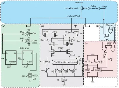
Fig 3.1 (a) CMOS Volatile D-latch, (b) 4-bits STT-MRAM including Sense Amplifier circuit (c) STT writing circuit, (d) Self-Enable control circuit, (e) Power gating cell using sleep p-MOS transistor (header switch).
IV.OPERATION OF MAGNETIC FF
4.1 CMOS FLIP-FLOP (CFF)
ISSN (Print) : 2320 – 3765 ISSN (Online): 2278 – 8875
I
nternational
J
ournal of
A
dvanced
R
esearch in
E
lectrical,
E
lectronics and
I
nstrumentation
E
ngineering
(An ISO 3297: 2007 Certified Organization)
Vol. 3, Issue 11, November 2014
10.15662/ijareeie.2014.0311079
4.3 CONVENTIONAL BIDIRECTIONAL STT-MRAM WRITING CIRCUIT
In conventional writing circuit for STT-MRAM write operation SWE_bar=0, the transistors MN4 and MN5 are turned off to isolate between the read and the write operations so that the read current will not be disturbed by the write current. To write logic ‘0’ the transistors MP4 and MN7 are turned on and the transistors MP5 and MN6 are turned off, the write current generated flows. To write logic ‘1’, the reversed current is generated by turning on theMP5 and MN6 and turning off the MP4 and MN7.The switching may happen at any moment inside the large fixed write pulse, in addition the write current is applied to all p-MTJs even when the current p-MTJ state “Qm” is equal to the expected data “Qs”. Therefore, unnecessary energy is lost. The energy to store “0101” is 4.5pJ from this simulation. In order to save this wasted energy while keeping high data reliability, add a small combinatory logic block to build up a self-enabling write circuit is shown in fig 3.1(c).
4.4 SELF-ENABLE CONTROL CIRCUIT
The “Self-Enable” circuit is to replace the fixed writing pulse by a sequence of self-enabled write/read operations. The schematic of the self-enabled switching circuit is shown in fig 3.1(d). By activating CKP=1 , the self enabled SWE_bar=0, the current p-MTJ state “Qm” and the expected state “Qs” are different, and no sensing operation is ongoing SE=0. The switching pulse is applied when “Qm” is equivalent to “Qs”. If there is a read back, the switching current is applied only forNm bits where “Qs” is different to “Qm”. The switching energy reduction Es can be calculated using self enable technique. In our simulation the four p-MTJs are initialized at logic ‘1111’ and the expected data “Qs” is ‘0 1 0 1’. In fact, only two out of four bits are written. The energy reduction is estimated and the write energy of the four p-MTJs is reduced.
4.5 POWER-GATING CIRCUIT
To simplify the PG mechanism and conserve area, the writing circuit of all the transistors are sized to reduce the write supply voltage to Vdd logic. Therefore, all blocks are powered by the same logic Vdd (1.1 V), and share the same sleep transistor. During the standby mode the MFF can be fully shut down and the leakage power can be completely suppressed. As different logic blocks will not switch simultaneously, at the same time the peak current will not occur, the sleep transistor can be trimmed to save area. Once the standby mode is detected, the “sleep” signal is activated and the checkpoint “CKP” is forced. The delay will depend only on the writing latency of STT-MRAM (e.g.4 ns/bit) . Power gating shows the simulated waveform for MFF power gating and different operations before and after the cutting-off power is shown in the Fig.3.1(e).
V. PROPOSED SYSTEM
LECTOR is used for reducing the leakage power based on the effective stacking of transistors in the path from supply voltage to ground. The LECTOR technique is based on the concept that “a state with more than one transistor OFF in a path from supply voltage to ground is far less leaky than a state with only one transistor OFF in any supply to ground path.” In this process, two leakage control transistors (LCTs) were introduced in each CMOS gate, a PMOS (LCT1) added to the pull-up network and a NMOS (LCT2) added to the pull-down network and the gate terminal of one LCT is controlled by the source terminal of the other, such that one of the LCTs is always near its cutoffregion of operation for any input(s) given to the CMOS gate, thus providing additional resistance in the path from supply to ground, decreasing the sub-threshold leakage current, thereby the reducing the static power.
VI. WORKING PRINCIPLE OF LECTOR
ISSN (Print) : 2320 – 3765 ISSN (Online): 2278 – 8875
I
nternational
J
ournal of
A
dvanced
R
esearch in
E
lectrical,
E
lectronics and
I
nstrumentation
E
ngineering
(An ISO 3297: 2007 Certified Organization)
Vol. 3, Issue 11, November 2014
LCT1 completely to OFF state the voltage is not sufficient. Hence, the resistance of LCT1 will be lesser than it’s OFF resistance, allowing conduction. Even though the resistance of LCT1 is not as high as it’s OFF state resistance, it increases the resistance of Vdd to ground path, controlling the flow of leakage currents, and then the leakage power has been suppressed and saves the static power.
Fig.6.1 Lector technique
ISSN (Print) : 2320 – 3765 ISSN (Online): 2278 – 8875
I
nternational
J
ournal of
A
dvanced
R
esearch in
E
lectrical,
E
lectronics and
I
nstrumentation
E
ngineering
(An ISO 3297: 2007 Certified Organization)
Vol. 3, Issue 11, November 2014
10.15662/ijareeie.2014.0311079 Fig 7.2 simulation result of LECTOR technique
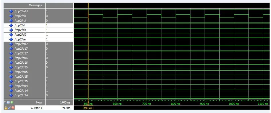
The fig 7.2 shows that the performance of LECTOR technique is better as compared to MFF. Two mechanisms were employed to achieve ultra low power consumption. The first one is the checkpointing/power-gating operation used to suppress the stand by static leakage power by cutting off the power supply voltage. The second one is the Self-Enable switching, which can reduce significantly the large margin of the switching current to avoid errors driven by the intrinsic stochastic effects of STT. By using LECTOR technique, leakage power has been reduced from 40nw to 25nw.
VIII. CONCLUSION
The scaling down of device dimensions, supply voltage, and threshold voltage for achieving high performance and low dynamic power dissipation has largely contributed to the increase in leakage power dissipation. we proposed a new magnetic flip-flop (MFF) integrating four contexts with little area overhead. It can be used as a key element in the future memory hierarchy architectures to achieve a “normally off” computing system. To achieve ultra low power two mechanisms has been used. The first one is the checkpointing/power-gating operation used to suppress the standby static leakage power by cutting off the power supply voltage. The 3D structure of STT-MRAM allows the checkpointting operation to achieve tradeoff between speed and energy. The second one is the Self-Enable switching, is to reduce significantly the large margin of the switching current to avoid errors. This paper presents “LECTOR” to tackle the leakage problem. LECTOR uses two additional self controlled transistors. Like other leakage reduction techniques, such as sleepy stack, sleepy keeper, etc, LECTOR also achieves leakage power reduction but with the advantage of not affecting the dynamic power as this technique does not require any additional control and monitoring circuitry like in and also maintains exact logic state. Comparing to CFF and STT-MRAM power has been consumed but has high static power. Using LECTOR technique leakage current suppressed and saves the static power is shown in fig 7.2.
ISSN (Print) : 2320 – 3765 ISSN (Online): 2278 – 8875
I
nternational
J
ournal of
A
dvanced
R
esearch in
E
lectrical,
E
lectronics and
I
nstrumentation
E
ngineering
(An ISO 3297: 2007 Certified Organization)
Vol. 3, Issue 11, November 2014
REFERENCES
[1] Djaafar Chabi, Weisheng Zhao,Member, IEEE, Erya Deng, Yue Zhang, Student Member, IEEE, Nesrine Ben Romdhane, Jacques-Olivier Klein, Member, IEEE, Ultra Low Power Magnetic Flip-Flop Based on Checkpointing/Power Gating and Self- EnableMechanisms-2013.
[2] K. Andoet al., “Roles of non-volatile devices in future computer system: Normally-off computer,”IGI Global, pp. 83–107, Jun. 2012.
[3] E. Deng, Y. Zhang, J. O. Klein, D. Ravelosona, C. Chappert, and W. S.Zhao, “Low power magnetic full-adder based on spin transfer torque MRAM,” IEEE Trans. Magn., vol. 49, pp. 4982–4987, 2013.
[4] H. Yodaet al., Progress of STT-MRAM Technology and the Effect on Normally-Off Computing Systems Session 11.3, IEDM 2012.
[5]X.Wu,W.Zhao,M.Nakamoto,C.Nimmagadda,D.Lisk,S.Gu,R.Radojcic, M. Nowak, and Y. Xie, “Electrical characterization for intertier connections and timing analysis for 3-D ICs,”IEEE Trans. Very Large Scale Integr. (VLSI) Syst., vol. 20, no. 1, pp. 186–191, 2012.