Volume 2008, Article ID 830273,12pages doi:10.1155/2008/830273
Research Article
An MC-SS Platform for Short-Range Communications in
the Personal Network Context
Dominique Noguet,1Marc Laugeois,1Xavier Popon,1B. Balamuralidhar,2Manuel Lobeira,3
Narasimha Sortur,2Deepak Dasalukunte,4Cedric Dehos,1and Zeta Bakirtzoglou5
1Leti Minatec Center (CEA), 17 rue des Martyrs, 38054 Grenoble Cedex 9, France
2Tata Consultancy Services Limited (TCS Limited company), 96 Epip-ip Industrial Area, Whitefield Road 560066, Bangalore, India 3ACORDE S.A., Centro de Desarrollo Tecnol´ogico, Avenida de los Castros S/N, 39005 Santander, Cantabria, Spain
4Department of Electrical and Information Technology, Lund University, P.O. Box 118, 22100 Lund, Sweden 5Intracom S.A. Telecom Solutions, 19.7 km Markopoulou Ave, 19002 Peania Attika, Greece
Correspondence should be addressed to Dominique Noguet,dominique.noguet@cea.fr
Received 4 June 2007; Revised 8 September 2007; Accepted 16 December 2007
Recommended by Luc Vandendorpe
Wireless personal area networks (WPANs) have gained interest in the last few years, and several air interfaces have been proposed to cover WPAN applications. A multicarrier spread spectrum (MC-SS) air interface specified to achieve 130 Mbps in typical WPAN channels is presented in this paper. It operates in the 5.2 GHz ISM band and achieves a spectral efficiency of 3.25 b·s−1·Hz−1. Besides the robustness of the MC-SS approach, this air interface yields to reasonable implementation complexity. This paper focuses on the hardware design and prototype of this MC-SS air interface. The prototype includes RF, baseband, and IEEE802.15.3 compliant medium access control (MAC) features. Implementation aspects are carefully analyzed for each part of the prototype, and key hardware design issues and solutions are presented. Hardware complexity and implementation loss are compared to theoretical expectations, as well as flexibility is discussed. Measurement results are provided for a real condition of operations.
Copyright © 2008 Dominique Noguet et al. This is an open access article distributed under the Creative Commons Attribution License, which permits unrestricted use, distribution, and reproduction in any medium, provided the original work is properly cited.
1. INTRODUCTION
Personal Networks (PNs) are a recent paradigm that en-able an individual to experience connectivity with his de-vices with unrestricted geographic span [1]. This network concept is leveraged by the availability of reliable wireless links between the devices in the user vicinity. The analysis of user’s needs carried out in [2] has shown two typical classes of applications that can be differentiated by the data rate range; they require low data rate (LDR), lower than 250 kbps and high data rate (HDR), up to 100 Mbps. Other studies have shown that due to specific channel conditions and more specifically its dynamicity [3,4], a specific attention must be taken in the design of the physical layer (PHY) of these inter-faces. New air interfaces have been specified for short-range, very high data rate applications, under the framework of the IEEE802.15.3 standard. However, a consensus could not be reached on a single solution among the systems that were proposed. One of the most famous systems is probably
Wi-Media which targets 480 Mbps using multiband orthogonal frequency-division multiplexing (OFDM) [5]. New trends in regulation (e.g., [6]) indicate that the future worldwide band for ultra-wideband operation will move to higher fre-quency though leading to more power consuming and costly implementation. Besides, most of the applications foreseen require either lower data rate or far higher like wireless high-definition multimedia interface (HDMI).
Channel
Figure1: PHY functional block diagram.
Synchro.
Figure2: PHY frame format.
access (CDMA) approaches when many asynchronous users are sharing the same band. Moreover, this air interface ex-hibits a very high degree of flexibility from which link adap-tation techniques can benefit [9].
This paper focuses on the design of a hardware platform for up to 130 Mbps operating in the 5.2 GHz ISM band. Its MAC layer is compliant with the IEEE802.15.3 standard [10]. A real-time implementation of the PHY layer runs on an FPGA and a wideband radio front-end providing over the air interface. The paper is divided into 6 sections. InSection 2, a short description of the air interface and the related param-eters is given. In Section 3, some aspects of the MAC pro-tocol and its implementation are detailed. InSection 4, the baseband processing hardware design is described and com-plexity issues are discussed. InSection 5, the radio front-end selection is discussed. InSection 6, the global hardware ar-chitecture and platform are described. Finally,Section 7 pro-vides measurement results obtained with the prototype.
2. OVERVIEW OF THE SELECTED MC-SS SYSTEM
The MC-SS air interface detailed in this paper, referred to as the MAGNET HDR (M-HDR), has been optimized for wire-less personal area networks (WPANs) in the PN context. Un-like cellular and wireless LAN systems, peer-to-peer commu-nication (especially from data traffic point of view) will hap-pen in such a context. In this case, simultaneous communi-cation between different users will yield to high interference for which CDMA would require high complexity multiuser detectors, which is not compliant with the low complex-ity requirement of the M-HDR system. Therefore, a TDMA scheme was chosen. This scheme also has the advantage of being compliant with the IEEE802.15.3 standard. Regarding the PHY, the M-HDR air interface is based on multicarrier technology capable of transmitting data from low to high rate for WPAN environment. An overview of the baseband PHY operations is illustrated by the block diagram ofFigure 1.
The M-HDR is based on a coded OFDM modulation us-ing convolutional coder. The data are spread over the sub-carriers by the spreading and multicode blocks. This func-tion aims at a better exploitafunc-tion of channel diversity, thus yields to more robustness [7]. Preamble information is then appended in the time domain to build the PHY frame struc-ture described inFigure 2.
At the input of the receiver, automatic gain control (AGC) and time/frequency synchronization are performed in the time domain. The synchronization block, which is critical in OFDM systems, is detailed in Section 4. After the OFDM demodulation, the channel is estimated using a least square estimator over full pilot symbols. This is based on the assumption of low device velocity in WPAN con-text. After the despreading, the bits are demapped from the QPSK, 16-QAM, or 64-QAM, according to the mode selected. The range of data rate envisaged is from few of Mbps to 130 Mbps, which corresponds to HDR-WPAN sce-narios identified in the MAGNET project [2]. Two modes of operations using 20 MHz and 40 MHz bandwidth han-dling up to 65 and 130 Mbps, respectively, are considered for additional flexibility. The maximal spectral efficiency of 3.5 bits·s−1·Hz−1is achieved using the 64-QAM. Detailed
rationale for parameters is given inTable 1, choices can be found in [7,10].
3. MAC PROTOCOL
Table1: MC-SS air interface main parameters.
40 MHz 20 MHz
Carrier frequency 5.20 5.20 GHz
Sampling frequency 40 20 MHz
FFT size 256 128
Total subcarriers 256 128
Subcarriers for guard band 45 23
Subcarriers for pilot 19 9
Subcarriers for data 192 96
Percentage of guard band 17.578 17.969 %
Subcarrier spacing 156.250 156.250 kHz
Occupied signal bandwidth 33.13 16.56 MHz
Number of time samples per data symbol 256 128 samples
Samples for guard interval 10 5 samples
Samples for total OFDM burst 266 133 samples
Maximum delay spread 0.213 0.213 μs
Sample duration in time 0.025 0.050 μs
Length of data interval in time 6.40 6.40 μs
Length of guard interval in time 0.250 0.250 μs
Length of total OFDM interval in time 6.65 6.65 μs
Percentage of guard interval 3.91 3.91 %
Channel coding Convolution code
Generator polynomial G1=133, G2=171
Tail 6 bits
spreading factor 8 8 chips
Maximum velocity 3 3 Km/h
Maximum doppler spread 14.4 14.4 Hz
Coherence time=9/(16π fD) 12.4 12.4 ms
Higher layer M-HDR MAC
APIs Control Data
Host interface
module
Host (Nokia 770)
USB
USB
host
USB
de
vi
ce
Target module
NIC
Figure3: M-HDR MAC implementation architecture.
From the implementation point of view, the following three modules were implemented.
(1) The M-HDR MAC module contains the implemen-tation for the core MAC functionalities, for example, beacon transmission for piconet formation, channel scanning for piconet discovery, synchronization with other devices, association/disassociation requests to join and leave piconet, and asynchronous/isochronous data transmission. On the data path, this module ex-changes logical link control (LLC) frames with the
host while the control path is used to exchange vari-ous management commands, for example, set or fetch configuration parameters. In order to achieve the re-quired real-time performance, the MAC is partitioned into hardware (HW-MAC) and software (SW-MAC). The time-critical and compute-intensive blocks like CRC generation and ciphering are implemented in hardware as part of HW-MAC. In the following sub-sections, we elaborate on both the software and hard-ware parts of the MAC implementation.
(2) The target module ofFigure 3acts as an interpreter for the messages it receives from the host over the USB link. It translates these commands into IEEE-802.15.3 format and forwards them to the M-HDR MAC mod-ule for further processing.
(3) The host interface module implements the application programmable interfaces (APIs) which are used by the higher layers to access various MAC functionalities.
0 1 3 · · · 2048
Frame identifier Payload size Payload
Figure4: Frame format for message exchange between the host and HDR NIC.
Host interface
Frame convergence
sublayer
Device management
entity
M-HDR MAC
Transmitter chain
Receiver chain
Transmitter Receiver
IOCTL
CAP, CTA queues
Device driver
Baseband TX Baseband RX handler
Beacon handler
ISR
Baseband
Figure5: Architecture of the IEEE802.15.3 MAC.
As mentioned above, the implementation of the M-HDR MAC conforms to the IEEE802.15.3 standard and consists of the four main building blocks (seeFigure 5).
3.1. SW-MAC design
Non-real-time critical features of the MAC are implemented on a software (SW-MAC) running on an embedded general purpose processor (GPP).
The TX-frame processing block is mainly responsible for the formation of the data and command frames to be trans-mitted. Upon receiving the data/command request from the frame convergence sublayer (FCSL) or the device manage-ment entity (DME), the transmitter chain validates the re-quest, for example, the sourceid, dstid, data length, and stream index parameters. The MAC frame prepared by at-taching the MAC header and the payload is then sent to the transmitter for the transmission over the air.
The transmitter block puts these frames into appropri-ate device driver queues for transmission. The device driver implements two transmission queues: one for transmissions during the contention access period (CAP) and the other for transmissions during the allocated channel time (CTA).
The RX-frame processing module is responsible for re-ceiving the frames from the baseband and forwarding them to the FCSL or DME. The receiver upon receiving the frame from the baseband verifies the frame for the command or the data. The command frames are forwarded to the DME block and the data frames are passed to the FCSL block.
The receiver block coordinates the packet reception be-tween the receiver chain and the baseband device driver.
Baseband
initMac()
DME RX
FCSL TX frames RX frames TX
Figure6: A multithreaded implementation.
by the use of semaphores. The Linux system calls are imple-mented as a thin operating system abstraction layer (OSAL). The OSAL implements the generic wrapper functions over the OS-dependent system calls.
As shown inFigure 6, the M-HDR MAC module is im-plemented as a multithreaded program. The module is ac-tivated by a call to the main function which in turn in-vokes the initMAC() function. The initMac() function ini-tializes the framework by creating the threads for each of the DME, FCSL, transmitter chain, receiver chain, as well as the transmitter and the receiver blocks. The associated message queues, registers, memory pool, and PIB (PAN Information Base) parameters are also initialized.
3.2. HW-MAC primitives
The hardware MAC (HW-MAC) is present at the interface between the PHY layer and the SW-MAC layer. It inher-its some terminal functions of the MAC layer to achieve improved real-time performance as compared to that per-formed when in software. The HW-MAC handles all the data processing in order to provide the PHY layer with the re-quired format of the packet to be transmitted . Similarly, the HW-MAC receives packet from PHY BB and transforms it in a consistent way for the SW-MAC . The HW-MAC consists of several blocks like the hardware 128 bit advanced encryption standard (AES) unit which benefits from the implementa-tion described inFigure 7, CRC generation/verification units and register address space along with an address decoder. The top-level finite state machine is the intelligence behind the working of HW-MAC. It schedules and synchronizes the data flow between SW-MAC and PHY BB depending on the type of configuration defined by the SW-MAC.
The block diagram of the HW MAC depicting the flow of data between SW-MAC and PHY BB is shown inFigure 7. The presence of HW-MAC makes the SW-MAC perceive the PHY layer as any other peripheral. This is because the HW-MAC provides the SW-HW-MAC with an interface similar to a memory. Various configurations and status registers includ-ing the data and header FIFOs are mapped on to an address space to which the SW-MAC can write. If the SW-MAC re-quires transmitting a data packet over the air, it writes the configuration in the registers and the data to be transmitted into the FIFOs. The HW-MAC delivers it to the PHY layer according to the configuration set by the SW-MAC. Con-versely, when a packet is received from the PHY layer and if it is intended for a device in receive mode, the HW-MAC
ver-ifies the packet for its integrity and interrupts the SW-MAC to inform about the received packet. Besides these schedul-ing functions, the HW-MAC also implements primitives to speed up the computation of data. This concerns encryption, CRC generation/verification, and other minor functions like packet parsing, packet formatting, timers, and so on.
4. BASEBAND PROCESSING
Like any OFDM system, the M-HDR air interface is sensi-tive to synchronization error and a particular attention has been made to handle robust synchronization at the receiver. Another specific concern for real-time digital design of the M-HDR air interface is clock-domain management. Finally, hardware implementation errors (e.g., quantization noise, operator bias, etc.) impact on processing precision needs to be quantified. Implementation loss induced by the baseband processing is scarcely addressed in the literature. In this sec-tion, the error introduced by the digital baseband processing is quantified and its impact is given in terms of equivalent additive white Gaussian noise (AWGN) signal on the ideal signal.
4.1. Synchronization
The synchronization aims at referencing in time the FFT vec-tor for OFDM demodulation and at estimating the carrier frequency offset (CFO) in the time domain (pre-FFT). CFO corresponds to the TX/RX oscillator frequency shift. Correct-ing the CFO is of paramount importance for OFDM systems which are very sensitive to such an impairment [8]. Synchro-nization is processed on the fly and runs continuously once the AGC is locked. It seeks a specific synchronization pattern contained in each frame header [10]. The synchronization process is ruled by a finite state machine (FSM) whose state is updated every received sample. It synchronizes the data flow according to the strongest path of the channel which is used as time reference.
The time synchronization is performed as follows. First, the autocorrelation of the received signal is computed. The periodic nature of the synchronization pattern enables the autocorrelation to show a typical flat region when the syn-chronization symbol is received. When the flat region is de-tected, the synchronization sample is coarsely indexed. To refine the position detection, a more restricted window is considered and the cross-correlation of the input signal with the known synchronization pattern is analyzed throughout this window. Peaks appear on the cross-correlation profile as soon as the known pattern is completely received. As previ-ously stated, criterion to detect those peaks is defined. When last cross-correlation peak is received, the system can be syn-chronized accurately. In fact, the window is active when the autocorrelation signal is higher than the threshold over more than a predetermined time. This time is related to the syn-chronization pattern duration.
SW
-MA
C
TX FIFO
RX FIFO
Config./status registers
Global controller
AES
HW-MAC
CRC
CRC
Packet formatted TX FIFO
Addr. verif.
Packet parsing
PH
Y
B
B
Figure7: HW-MAC block diagram.
1E−06 1E−05 1E−04 1E−03 1E−02 1E−01 1E+ 00
0 0.2 0.4 0.6 0.8 1
False alarm and misdetection probability
Auto correlation threshold
PMD SNR=2 dB PMD SNR=8 dB PMD SNR=14 dB PMD SNR=4 dB
PMD SNR=10 dB PFA
PMD SNR=6 dB PMD SNR=12 dB Figure8: False alarm and misdetection probability.
an AWGN channel. The threshold is represented as a percent-age of the maximum value of the autocorrelation.
The PFA is defined as the probability of finding a syn-chronization sample while no synsyn-chronization symbol was transmitted. Obviously, it decreases when the autocorrela-tion threshold increases. The PFA does not depend on the signal-to-noise ratio (SNR). This is due to the fact that the flat region is never detected when no synchronization pat-tern is sent, whatever the noise level.
The PMD is defined as the probability of missing the synchronization point despite the transmission of a synchro-nization symbol. For the lowest thresholds, the misdetection is mainly due to bad flat region localization or, as for the false alarm, due to the absence of autocorrelation flat re-gion falling edge. For high thresholds, misdetection is also high but mainly due to nondetection of the flat region. Be-tween these two threshold regions, a minimum is obtained around 0.5.
A PFA versus PMD, tradeoffvalues can be obtained for each SNR as the crossing point of the misdetection and false alarm curves. For instance, the SNR=8 dB provides PFA< 10−5and PMD<10−5choosing the threshold equal to 68%.
When higher SNR are targeted, increasing the threshold will reduce the false alarm probability. For 10 dB, setting a 70% threshold brings about PFA<10−6and PMD<10−6.
4.2. Clock management for flexible design
Bringing flexibility of the baseband in terms of data rate in-creases the complexity of clock management. This section describes clock management and its impact on hardware ar-chitecture tradeoffs. The focus is on the 40 MHz system but can be transposed to the 20 MHz case easily. The convolu-tional encoder is fed with data at frequency f. The coder produces two parallel bits which are serialized before being punctured. LetNbe the number of bits per symbol,Dthe serial output data rate of the convolutional encoder,Rthe global code rate,P the puncturing rate, and f the working frequency if only one frequency was used in the design. Since each OFDM symbol of 266 samples carries 192 data, the se-rial bitrate at the output of the coder isD = 192×40× N/266≈29×N. At the output of the puncturing, the data are at the frequency f.Table 2recaps the frequency to be used at the coder module according to the MAGNET modulation scheme implying different clock frequencies. The solution to dynamically change clock frequencies to address these modes is to use XILINX Virtex 4 tunable DLL feature.
Table2: Convolutional encoder frequencies.
Modulation N R D P f Nb bit/OFDM symbol
Coder input Coder output
QPSK 2 1/2 58 1 58 192 384
QPSK 2 3/4 58 2/3 87 288 384
16 QAM 4 1/2 116 1 116 384 768
16 QAM 4 3/4 116 2/3 174 576 768
64 QAM 6 2/3 174 3/4 232 768 1152
64 QAM 6 3/4 174 2/3 261 864 1152
MAC-SW
FIFO
Ins PHY header
FIFO
MAC-SW
Programmable DCM frequencyf
DCM 174 MHz
DCM
174/6=29 MHz Framing
DCM 40 MHz
Channel
coding FIFO S→P Interleaver Mapping
Multicode
spreading FIFO
OFDM modulation
Time domain preamble
RAM
Cyclic prefix insertion
MC-SS transmitter
Programmable DCM frequencyf /2
DCM 174 MHz fandf /2
DCM
174/6=29 MHz estimationChannel Synchronisation
Channel
decoding FIFO
P→S
depunc Deinterleaver
Soft demapping
Multicode
despreading FIFO Egalisation
OFDM demodulation & deframinig
DCM 40 MHz
MC-SS receiver
Bit level signal 6 bits level signal Signed signal
Figure9: M-HDR baseband clock management.
serial to parallel converter always works at the highest fre-quency, and the data validation signal duty cycle is adjusted according to the modulation. This choice leads to a very small part of the design working at high frequency that does not need to be changed according to the modulation. The map-per and the spreader, that follow, process at the modulation symbol rate, namely, 29 MHz. Then, pilots are inserted in-creasing the rate up to 40 MHz for the OFDM modulation.
Figure 9shows the resulting clock domains.
5. RF FRONT-END
For the M-HDR platform, several receiver front-end archi-tectures have been considered, two of which have emerged as possible candidates. On one hand, a classical zero interme-diate frequency (zero-IF), and on the other hand, a modi-fied weaver [11] which achieves a rejection of the image fre-quency, are generated by the down conversion of a hetero-dyne receiver.
As it is known, the weaver architecture is first mixed with the quadrature phases of the local oscillator to be then
low-pass filtered (see Figure 10, in which IF = RF1 −LO =
LO−RF2, where RF1is the desired signal and RF2the image
frequency that would lead to the same IF after the synthesis). One drawback of this architecture is that it introduces the problem of a secondary image, if the second mixer translates the spectrum to a nonzero frequency. With the frequency plan considered for the M-HDR system, this effect may cause UMTS image frequency to interfere with the desired signal.
The performance of the modified weaver architecture in terms of rejection depends on the phase and gain mismatch between the two reception paths. For a 1–5◦phase mismatch or 0.2–0.6 dB gain mismatch, it was reported that such archi-tecture achieves 30–40 dB rejection [12].
The parameters of the second approach, the zero-IF-based architecture, are specified in Figure 11. The global noise factor is similar to the one of the weaver architecture.
3.6 GHz (0◦) 1.6 GHz (0◦)
5.2 GHz
LNA BPF
1.6 GHz 2 GHz image
1.6 GHz 2 GHz rejected
NF0,G0
NF1,G1 NF2,G3 NF3,G3 NF4,G4 NF5,G5
+
NF6,G6
VGA
LNA BPF
3.6 GHz (90◦) 1.6 GHz (90◦)
NFtotal=NF0+NF1−1 G0
+NF2−1
G0.G1
+ NF3−1
G0.G1.G2
+ NF4−1
G0.G1.G2.G3
+ NF5−1
G0.G1.G2.G3.G4
+ NF5−1
G0.G1.G2.G3.G4.G5
Figure10: Weaver RF architecture.
5.2 GHz
LNA
NF0,G0
NF1,G1 NF2,G2
NF3,G3
NF3,G3
VGA/filter 5 GHz (0◦)
5 GHz (90◦)
Antenna:
Noise figure (loss): 0.5 dB Phase Error: 0.5
Gain error (imbalance): 0.1 dB Gain: 0 dB
Impedance: (matched to LNA)
RF filter:
Noise figure: 1.5 dB Gain:−2 dB
Adjacent channel rejection: 30 dB VGA/filter:
Noise figure: 20 dB Gain: 10–60 dB
Adjacent channel rejection: 30 dB LNA:
Noise figure: 5 dB
1 dB compression point:−25 dBm IP2: 70 dBm
IP3:−15 dBm
Phase error: 20 (discrete) 10 (integr.)
Gain error: 0.2 dB Gain: 20 dB
Mixer:
Noise figure: 8 dB Isolation; LO to RF: 30 dB LO to DC: 27 dB RF to DC: 40 dB IP2: 25 dBm IP3: 5 dBm Phase error: 20 Gain error: 0.2 dB Gain: 10 dB
A.N.:NFtotal=5.2 dB NFtotal=NF0+NFG1−1
0 +
NF2−1 G0.G1 +
NF3−1 G0.G1.G2+
NF4−1 G0.G1.G2.G3+
NF5−1 G0.G1.G2.G3.G4
Figure11: Zero-IF RF architecture.
filter, and the digital filter. On the other hand, since the chan-nel and image coincide due to the direct conversion, the zero-IF architecture does not suffer from image rejection is-sue. This latter point is more critical for the weaver archi-tecture that implements an “explicit” rejection scheme. The conclusion that can be drawn is that provided the same
Host
Digital board RF board
Figure12: Platform block diagram.
RF connection
Figure13: M-HDR prototype: (a) digital side and host PDA; (b) RF daughter board side and antenna.
1E−05
Figure14: Impact of fixed point computation for noncoded QPSK configuration.
direct conversion. However, since the DC subcarrier is not used by the baseband, DC offset is no longer a very critical is-sue if enough attention is paid to the frequency stability and phase noise. Perfect channel and CFO (ref.) With CFO estimation With channel estimation With channel and CFO estimation
Figure15: Impact of CFO and channel estimation for noncoded QPSK configuration.
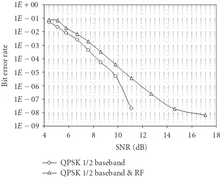
1E−09 QPSK 1/2 baseband & RF
Figure16: Impact of RF front-end for QPSK-1/2 configuration.
by a random phase shift in the time domain (before FFT). The influence of the phase noise in the OFDM signal appears in two different ways in the frequency domain as reported in [13].
(1) A common phase error (complex value) is multiplied to all subcarriers. This error comes from close-to-carrier phase noise. This error can be tracked and re-moved by equalization.
(2) Due to further carrier phase noise, subcarriers are mixed together at FFT process, by such a way, inter-carrier interference appears as hardly removable extra-noise in the signal.
These should lead to a tradeoffbetween signal processing ex-tracomputation (common phase error tracking) and require-ments on the PLL and crystal choices.
Innovative design works [14–17] presented different techniques that provided improved reliability and a yield of CMOS RF transceivers, what has made, after the proper evo-lution in the research areas, CMOS process a real player in the cost-effective radio market. Single-chip solution offers as well several advantages such as reduction in manufacturing and packaging costs due to the elimination of the routing be-tween different integrated circuits, leading to a printed circuit board (PCB) multilayer complexity reduction. Smaller ar-eas and diminished consumption (simplification of internal interfaces between blocks) jointly with shorter factory test times and higher test yields are other benefits of the single-chip designs. For these reasons, the zero-IF approach was preferred and the MAXIM MAX2829 chip was used as the heart of the RF part of the design. Besides, the included PLL bandwidth and the chosen crystal reference made negligible the extradistortion caused by the phase noise effects.
6. IMPLEMENTATION PLATFORM
The M-HDR prototype consists of a set of boards that em-bed the components needed for the implementation of MAC and PHY layers, namely, an RF board implementing TX and RX RF functions from/up to the converters up to/from
the antenna and a digital board implementing digital PHY and MAC functionalities. The latter also includes some host bridging features in order to plug the HDR prototype to a host device. An overview of the M-HDR prototype is illus-trated inFigure 12.
The HDR RF subsystem (or board) is based on an
off-the-shelf component from MAXIM (MAX2829). The
MAX2829 is designed for dual-band 802.11a/g applications covering especially world-band frequencies of 4.9 GHz to 5.875 GHz. The IC includes all circuitry required to imple-ment the RF transceiver function, providing a fully inte-grated receive path, transmit path, VCO, frequency synthe-sizer, and baseband/control interface. Only the power ampli-fier, RF switches, RF bandpass filters (BPFs), RF baluns, and a small number of passive components are needed to form the complete RF front-end solution.
The digital board houses the programmable chips that implement baseband PHY and MAC functions. For SW-MAC primitives, an ARM9 has been selected (AT91RM9200). The SW-MAC primitives run on top of a Linux OS. For the HW-MAC and PHY primitives, a Xilinx Virtex 4 has been chosen due to hardware resource available and flexible clock management capability (XC4VSX55-10). Complexity analysis that led to this chipset choices is pro-vided inTable 3. The NIC is used by its host as a USB device. Battery operation was made possible to enable handheld field trials. It offers autonomy of several hours. Power con-sumption is mainly due to FPGA implementation though an equivalent system-on-chip implementation would yield to dramatic power consumption decrease.
7. PHY MEASUREMENT RESULTS
This section aims at providing results of the tests performed with the M-HDR prototype. The first tests consist in bit er-ror rate (BER) versus SNR for different configurations of the platform, gradually illustrating the impact of each approxi-mation. Results presented hereafter are all given for AWGN channels for the sake of comparison.
The first step aims at evaluating the impact of fixed point implementation within the FPGA. It is worth mentioning that the converters (ADC) at the input of the receiver have a 12 bit dynamic introducing a quantization SNR of 72 dB. This means that the conversion noise is negligible within the SNR range addressed by the receiver. In order to see the im-pact of fixed point computation, the BER vresus SNR per-formance of the prototype was compared with the floating point simulation model. In both cases, measurements are performed under perfect channel estimation and without CFO estimation (both TX and RX share the same clock refer-ence and CFO estimator is disabled). The results are shown in
Figure 14for AWGN channel. From these noncoded perfor-mance curves, it can be noted that perforperfor-mance loss is negli-gible at the SNR range to be considered for the system.
1E−05 1E−04 1E−03 1E−02 1E−01 1E+ 00
Bi
t
er
ror
ra
te
4 6 8 10 12 14
SNR (dB) No mismatch
0.1/0.1 0.2/0.2
0.05/0.05 0.15/0.15
(a)
1E−05 1E−04 1E−03 1E−02 1E−01 1E+ 00
Bi
t
er
ror
ra
te
4 6 8 10 12 14
SNR (dB) No mismatch
0.1/0.1
With mismatch and correction (b)
Figure17: Impact of (a) IQ mismatch (lin/rad) and (b) IQ mismatch correction.
Table3: Complexity analyis.
(a)
PHY/MAC HW (FPGA) Logic (slices) Multipliers (18×18) Block RAM (18 kb) Clock domains (DCM)
Required for TX baseband 3800 18 30 4
Required for RX baseband 10200 118 49 4
Total required 14000 136 79 4
(b)
SW-MAC (Processor) Computational requirement ROM requirement RAM requirement
Requires for MAC ∼180 to 200 MIPS 8 64
noise. The previous curve obtained with perfect estimation is given as a reference. This reference curve is similar to the one ofFigure 14.
It can be observed that the major degradation is brought by the channel estimator linked to the zero-forcing equal-izer. However, the 3 dB shift is rather due to the kind of esti-mator chosen rather than its implementation, since floating point simulation provides similar results. It can be noticed that the CFO estimation and correction have little impact on the overall performance.
Measurements presented inFigure 16show the impact of the RF front-end to the global performance for the QPSK-1/2 configuration. It can be seen that the RF front-end introduces some degradation (e.g., around 1.5 dB shift at BER of 10−6).
At high SNR, an error floor of 10−8 cannot be overtaken.
Such error floor will impact the performance even further when weaker channel coding schemes will be used. Among the potential explanation for this phenomenon is the impact of IQ mismatch. IQ mismatch compensation schemes have been presented in the literature [13–15]. Simulations have provided information on the effects of the IQ mismatch and the frequency offset, as well as the capabilities of the correc-tion algorithms.
In the simulation results presented inFigure 17(a), the white noise coming from IQ mismatch intercarrier interfer-ence is higher than the front-end thermal noise. Error floor effects are then similar to those observed on the prototype. Results show a good BER improvement with IQ mismatch correction, even if IQ mismatch estimation is degraded at low SNR. InFigure 17(b), the corrected system curve meets the “no mismatch” curve.
8. CONCLUSION
The multicarrier spread spectrum prototype presented in this paper enables to achieve data rates that cover most WPAN applications necessities. Since the WPAN transceivers are likely to equip battery-operated devices, it is important that hardware complexity remains reasonable. The MC-SS air interface described herein has a complexity which is close to that of WLAN transceivers while achieving better robust-ness over WPAN channel conditions.
measurements have shown that the degradation introduced by the baseband implementation is compliant with simula-tion results. Measurements including the RF show that some error floor appears at high SNR values. Among the potential sources of degradation is the IQ mismatch. This impairment can be compensated at the baseband by efficient correction schemes that already proved their effectiveness through sim-ulation.
ACKNOWLEDGMENT
This work has been done in the frame of the MAG-NET Beyond European IST project of the 6th Framework Program. MAGNET Beyond is an R&D project within Mobile and Wireless Systems and Platforms Beyond 3G (www.ist-magnet.org).
REFERENCES
[1] A. Lo, W. Lu, M. Jacobsson, V. Prasad, and I. Niemegeers, “Per-sonal networks: an architecture for 4G mobile communica-tions networks,”Telektronikk Journal, 2007.
[2] R. Prasad and K. Skouby, “Personal network (PN) applica-tions,”Wireless Personal Communications, vol. 33, no. 3-4, pp. 227–242, 2005.
[3] IST-MAGNET project deliverable D3.1.2b, PAN Channel Characterisation, June 2005.
[4] J. Karedal, A. J. Johansson, F. Tufvesson, and A. Molisch, “Characterization of MIMO channels for handheld devices in personal area networks at 5 GHz,” inProceedings of the 14th European Signal Processing Conference (EUSIPCO ’06), Flo-rence, Italy, September 2006.
[5] J. D. P. Pav ´on, S. N. Shankar, V. Gaddam, K. Challapali, and C.-T. Chou, “The MBOA-WiMedia specification for ultra wide-band distributed networks,”IEEE Communications Magazine, vol. 44, no. 6, pp. 128–134, 2006.
[6] CEPT—ECC, “ECC Decision of dd mm 2006 on the har-monised conditions for devices usingUWB technology in bands below 10.6 GHz,” Draft (ECC/DEC/(06)AA) document 13 33-A8R0 Annex8 draft ECC Dec(06)AA Modifications proposed by TG3, February 2006.
[7] IST-MAGNET project deliverable D3.2.2, Candidate Air Inter-faces and Enhancements, December 2005.
[8] R. Prasad,OFDM for Wireless Communication Systems, Artech House, London, UK, 2004.
[9] K. Schoo, F. Bauer, and K. Strohmenger, “Adaptive modula-tion and coding in a PAN optimized air interface considering computation complexity,” inProceedings of the 15th IST Mobile Summit, Myconos, Greece, June 2006.
[10] IEEE 802.15.3 standard, Part 15.3: Wireless Medium Access Control (MAC) and Physical Layer (PHY) Specifications for High Rate Wireless Personal Area Networks (WPANs). [11] T. E. Dodgson, E. Lee, P. Gardner, and D. Noguet,
“Reconfig-urability in its application to platforms for private-personal area networks and personal networks,” inProceedings of the 15th Wireless World Research Forum, Paris, France, December 2005.
[12] IST MAGNET project deliverable D5.3.1 Selected air interface of PAN nodes for implementation, June 2005.
[13] L. Maret, C. Dehos, M. D.-N. Bouvier, D. Morche, and J. Bar-letta, “Sensitivity of a MC-CDMA beyond 3G sytem to RF im-pairments,” inProceedings of the 14th IST Mobile and Wireless Communications Summit, Dresden, Germany, June 2005. [14] R. L. Hovald,The communications performance of single-carrier
and multi-carrier quadrature amplitude modulation in RF car-rier phase noise, Ph.D. thesis, Drexel University, Philadelphia, Pa, USA, 1997.
[15] T. C. W. Schenk, E. R. Fledderus, and P. F. M. Smulders, “Performance impact of IQ mismatch in direct-conversion MIMO OFDM transceivers,” inProceedings of the IEEE Radio and Wireless Symposium (RWS ’07), pp. 329–332, Long Beach, Calif, USA, January 2007.
[16] K. Vavelidis, I. Vassiliou, T. Georgantas, et al., “A dual-band 5.15-5.35-GHz, 2.4-2.5-GHz 0.18-μm CMOS transceiver for 802.11 a/b/g wireless LAN,”IEEE Journal of Solid-State Cir-cuits, vol. 39, no. 7, pp. 1180–1184, 2004.