Grid Connected Photovoltic System Using
High Gain DC-DC Converter With Voltage
Multiplier Circuit
Nova Sunny, Santhi B
Department of Electrical and Electronics Engineering, Rajagiri School of Engineering and Technology
Kakkanad, India
Head of Department, Department of Electrical and Electronics Engineering, Rajagiri School of Engineering and
Technology, Kakkanad, India
ABSTRACT: In this paper, a high step – up converter which is suitable for renewable energy system connected to grid is proposed . Conventional step – up converters required for grid application cannot achieve high step – up conversion with high efficiency because of the resistances of elements or leakage inductance. The proposed converter is a conventional interleaved boost converter with voltage multiplier module which not only reduces the current stress but also constrains the input current ripple which decreases the conduction losses and lengthens the lifetime of the input sources.
KEYWORDS: high step-up, photovoltaic (PV) system, voltage multiplier module.
I. INTRODUCTION
Nowadays, renewable energy is increasingly valued and employed worldwide because of energy shortage and environmental contamination[1]-[3]. Renewable energy systems generate low voltage output, and thus, high step-up dc/dc converters have been widely employed in many renewable energy applications such fuel cells, wind power generation, and photovoltaic (PV) systems [4]-[6].Such systems transforms low voltage to high voltage via step up converter and produce ac using grid tie inverter. Fig 1 shows a typical renewable energy system that consists of renewable energy sources, a step-up converter, and an inverter for ac application. Output of renewable resources are very low ,in order to achieve grid application a very high input is required for the inverter. This can be achieved by using power electronics converters. In order to achieve high step up conversion, it may require two-stage converters with cascade structure for enough up gain, which decreases the efficiency and increases the cost. Thus, a high step-up converter is seen as an important stage in the system because such a system requires a sufficiently high step-step-up conversion with high efficiency.
Conventional converters like boost converter has limited step up gain and voltage stress across the switch is same as that of the output voltage. Despite these advances, high step-up single-switch converters are unsuitable to operate at heavy load given a large input current ripple, which increases conduction losses. The conventional interleaved boost converter is an excellent candidate for high-power applications and power factor correction. Unfortunately, the step-up gain is limited, and the voltage stresses on semiconductor components are equal to output voltage. Hence, based on the aforementioned considerations, modifying a conventional interleaved boost converter for high step-up and high-power application is a suitable approach.
Fig.1.Block diagram of photovoltaic system connected to grid
The proposed converter is a conventional interleaved boost Converter integrated with a voltage multiplier module, and the voltage multiplier module is composed of switched capacitors and coupled inductors. The coupled inductors can be designed to extend step-up gain, and the switched capacitors offer extra voltage conversion ratio which is required for grid application. In proposed scheme, PV array is tied with grid through Single phase Voltage source Inverter (VSI). High gain dc-dc converter is placed between PV array and inverter. The maximum power in PV array is tracked using incremental conductance based MPPT controller. The MPPT controller controls duty cycle of the converter. PLL is used to get the phase and frequency information of grid voltage.
II. SYSTEMDESCRIPTION
A. MODELING OF PV PANEL
By connecting the PV cells in series and parallel can produce desired output power. PV panel is modeled with the help of design equations. The terminal equation for the current and voltage of the array is given by
Np and Ns are no of parallel and series cells. Iph is the photocurrent ,Is is the cell saturation current,q is an electron charge and Tc is the working temperature, A is an ideal factor, Rsh is a shunt resistance and Rs is a series resistance of solar cell.
Iph = [Isc + Ki(Tc – Tref)] H
Where ,
Isc is the short circuit current, Ki is the short circuit current temperature coefficient ,Tref cell reference temperature and His the solar insolation in KW/m2
Cell’s saturation current varies with the cell temperature which is given by
Is = IRs (Tc/Tref)3exp[qEG(Tc – Tref)/TrefTckA
IRS is the cell’s reverse saturation current at a reference temperature and standard solar radiation. EG is the band gap energy of the semiconductor used in the cell.
B. Incremental conductance for MPPT
Incremental conductance Algorithm for mppt is used to track the maximum power Point (mpp) of the photovoltaic panels, and generate the control signal for the high gain dc- dc converter. The algorithm compares the actual conductance – Ipv/ Vpv and the incremental conductance dIpv/dVpv [7].
If dIpv/ dVpv. > – Ipv/ Vpv
Rsh
IRs
Ns
NpV
KTcA
Np
IRs
Ns
V
q
NpIs
NpIph
I
)
1
]
)
(
If dIpv/ dVpv. < – Ipv/ Vpv
then the operating point is on the right of the MPP, so α is varied to decrease Vpv
If dIpv/ dVpv. = – Ipv/ Vpv
then the operating point is in the MPP, so, the value of α is maintained.
where dIpv and dVpv are the PV current and voltage variations, respectively. Thus, the duty cycle α , used to generate
the PWM signal for the MOSFET switching.
III. HIGHSTEP-UPINTERLEAVEDCONVERTER WITH AVOLTAGEMULTIPLIERMODULE
A. HIGH GAIN DC – DC CONVERTER
The proposed high step-up interleaved converter with a voltage multiplier module is shown in Fig. 2. The voltage multiplier module is composed of two coupled inductors and two switched capacitors and is inserted between a conventional interleaved boost converter to form a modified boost–flyback–forward interleaved structure. When the switches turn off by turn, the phase whose switch is in OFF state performs as a flyback converter, and the other phase whose switch is in ON state performs as a forward converter. Primary windings of the coupled inductors with Np turns are employed to decrease input current ripple, and secondary windings of the coupled inductors with Ns turns are connected in series to extend voltage gain. The turn ratios of the coupled inductors are the same.
The equivalent circuit of the proposed converter is shown in Figure 3, where Lm1 and Lm2 are the magnetizing inductors, Lk1 and Lk2 represent the leakage inductors, S1 and S2 denote the power switches, Cb is the voltage-lift capacitor, and n is defined as a turns ratio Ns/Np. The duty cycles of the power switches during steady operation are interleaved with a 1800 phase shift and the key steady waveforms in one switching period of the converter contain six modes.
B . MODEL ANALYSIS
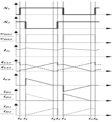
Operation of the converter can be explained in six modes. Steady state waveform is given in Fig4
Mode 1 [t0, t1 ]: At t= t0 , the power switches S1 and S2 are both turned ON. All the diodes are reversed-biased. Magnetizing inductors Lm1 and Lm2 as well as leakage inductors Lk1 and Lk2 are linearly charged by the input voltage source Vin.
Mode 2 [t1, t2]: At t= t1, the power switch S2 is switched OFF, thereby turning ON diodes D2 and D4. The energy that magnetizing inductor Lm2 has stored is transferred to the secondary side charging the output filter capacitor C3. The input voltage source, magnetizing inductor Lm2, leakage inductor Lk2, and voltage-lift capacitor Cb release energy to the output filter capacitor C1 via diode D2, thereby extending the voltage on C1.
Mode 3 [t2, t3 ]: At t= t2, diode D2 automatically switches OFF because the total energy of leakage inductor Lk2 has been completely released to the output filter capacitor C1. Magnetizing inductor Lm2 transfers energy to the secondary side, charging the output filter capacitor C3 via diode D4 until t3.
Mode 4 [t3, t4 ]: At t= t3 , the power switch S2 is switched ON and all the diodes are turned OFF. The operating states of modes 1 and 4 are similar.
Mode 5 [t4, t5]: At t= t4, the power switch S1 is switched OFF, which turns ON diodes D1 and D3. The energy stored in magnetizing inductor Lm1 is transferred to the secondary side charging the output filter capacitor C2. The input voltage source and magnetizing inductor Lm1 release energy to voltage-lift capacitor Cb via diode D1, which stores extra energy in Cb.
Mode 6 [t5, t0 ]: At t= t5, diode D1 is automatically turned OFF because the total energy of leakage inductor Lk1 has been completely released to voltage-lift capacitor Cb. Magnetizing inductor Lm1 transfers energy to the secondary side charging the output filter capacitor C2 via diode D3 until t0.
C. DESIGN
The electrical specifications are Vin = 40 V, Vo = 300 V, and fs = 40 kHz. The major components have been chosen as follows: Magnetizing inductors Lm1 and Lm2 =133 μH; turn ratio n = 1; capacitors Cc1, Cc2, C2, and C3 = 220 μF; and C1 = 470 μF.
Leakage inductors Lk1 and Lk2 are 1.6 μH.
IV.SINGLEPHASEDC–ACINVERTER
A full bridge inverter is used to convert DC voltage and current to AC voltage and current. The inverter is controlled by a PWM signal, which in turn controls the inverter switches[8] .
Fig.5 Single-phase full bridge inverter
V. SIMULATION
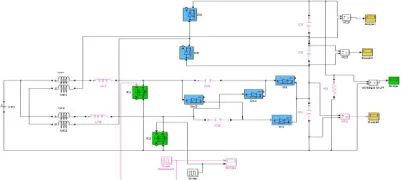
The system consist of solar panel, converter to step up the output voltage of solar panel ,inverter which is connected to single phase grid.
Fig 6. Simulation circuit of full system Fig7 Solar output voltage and current
Fig 8. Simulation circuit for high gain dc - dc converter Fig 9. Converter output voltage
Fig 11 SPWM generation Fig 10 Reference sine wave generation
Fig 12 Inverter circuit Fig 13 Control pulses for inverter switches
VI. CONCLUSION
The grid connected solar power plant can be done in place where excess solar energy is available. Simulation of photovoltaic system connected to single phase grid using high gain dc-dc converter is presented. By using this converter the duty ratio of power switches and power conversion rate can be maintained in an acceptable range. It shows high conversion rate as compared to conventional boost converter.
REFERENCES
[1] J. T. Bialasiewicz, “Renewable energy systems with photovoltaic power generators: Operation and modeling,” IEEE Trans. Ind. Electron., vol. 55,no. 7, pp. 2752–2758, Jul. 2008.
[2] T. Kefalas and A. Kladas, “Analysis of transformers working under heavily saturated conditions in grid-connected renewable energy systems,” IEEE Trans. Ind. Electron., vol. 59, no. 5, pp. 2342–2350, May 2012.
[3] Y. Xiong, X. Cheng, Z. J. Shen, C. Mi, H. Wu, and V. K. Garg, “Prognostic and warning system for power-electronic modules in electric, hybrid electric, and fuel-cell vehicles,” IEEE Trans. Ind. Electron., vol. 55, no. 6, pp. 2268–2276, Jun. 2008.
[4] S. K. Changchien, T. J. Liang, J. F. Chen, and L. S. Yang, “Novel high step-up DC–DC converter for fuel cell energy conversion system,” IEEE Trans. Ind. Electron., vol. 57, no. 6, pp. 2007–2017, Jun.
[5] Y. P. Hsieh, J. F. Chen, T. J. Liang, and L. S. Yang, “Novel high step up DC–DC converter with coupled-inductor and switched-capacitor techniques for a sustainable energy system,” IEEE Trans. Power Electron., vol. 26, no. 12, pp. 3481–3490, Dec. 2011.
[6] Y.-P. Hsieh, J.-F. Chen, T.-J. Liang, and L. S. Yang, “A novel high step-up DC–DC converter for a microgrid system,” IEEE Trans. Power Electron., vol. 26, no. 4, pp. 1127–1136, Apr. 2011.
[7] N. E. Zakzouk, M. A. Elsaharty, A. K. Abdelsalam, A. A. Helal and B. W. Williams, "Improved performance low-cost incremental conductance PV MPPT technique," in IET Renewable Power Generation, vol. 10, no. 4, pp. 561-574, 4 2016.
[8] Yahyaoui, F. Tadeo and M. V. Segatto, "Control strategy for small-scale photovoltaic systems connected to single-phase grids," 2016 7th International Renewable Energy Congress (IREC), Hammamet, 2016