Nitride Semiconductors: Bulk Crystals and Thin Films. (Under the direction of Dr. Zlatko Sitar and Dr. Ramon Collazo.)
As III-nitrides continue to evolve into a homoepitaxial growth scenario, the development of non-traditional metrologies for the proper study of III-nitride single crystals and homoepitaxial thin films becomes critical. To this purpose, the work presented in this dissertation has focused on the development and application of suitable high resolution X-ray diffraction (HRXRD) methods, desirable for their sensitivity, accuracy and non-destructive nature. HRXRD techniques were explored and developed for the identification of polishing-induced damage in processed III-nitride single crystals, the structural analysis of non-polar AlN homoepitaxial films grown on AlN single crystals and the assessment of alloy film characteristics of AlxGa1-xN epilayers deposited on AlN substrates.
AlN and GaN substrates were treated to various degrees of mechanical polishing and chemical mechanical polishing (CMP). Gross damage created from aggressive polishing was readily quantified using X-ray rocking curve (XRC) peak broadening and diffuse scatter intensity. However, once the wafers were exposed to CMP treatment, it was found that the use of line scanning methods was unable to distinguish the effects of CMP time exposure on the crystal surface. Alternatively, the analysis of surface-related diffraction features recorded from on- and off-axis high-resolution reciprocal space maps (RSMs) allowed the classification of remnant damage in CMP-treated substrates as a function of CMP exposure time. By comparing the crystal truncation rod intensity and the pole diffuse scatter magnitude, differences at the near-surface regions of CMP-processed wafers were qualitatively and quantitatively measured. For AlN, the mapping of the (101̅3) reflection, observable under grazing incidence conditions, was introduced as an effective HRXRD method to analyze the crystal surface of AlN substrates using a laboratory source.
measurements indicated that the films were strain-free. However, differences among the film surfaces were identified, corresponding to a transition from a heavily faceted step morphology to monolayer steps as the growth temperature was increased. To examine the presence of extended defects, defect-selective RSM analysis was performed using (ℎ0ℎ̅0) maps taken parallel to the [0001]. For all films, no characteristic broadening from basal plane stacking faults was observed. Additionally, for a two-layer AlN homoepitaxial structure, transmission electron microscopy under different diffraction conditions did not exhibit defect imaging contrast. These results evidence the ability to use HRXRD RSMs to characterize highly perfect non-polar m-plane AlN films.
by
Milena Rebeca Bobea
A dissertation submitted to the Graduate Faculty of North Carolina State University
in partial fulfillment of the requirements for the Degree of
Doctor of Philosophy
Materials Science and Engineering
Raleigh, North Carolina 2015
APPROVED BY:
_______________________________ ______________________________
Dr. Zlatko Sitar Dr. Ramon Collazo
Committee Co-Chair Committee Co-Chair
DEDICATION
BIOGRAPHY
ACKNOWLEDGMENTS
TABLE OF CONTENTS
LIST OF TABLES……… ix
LIST OF FIGURES……….. xi
CHAPTER 1: INTRODUCTION 1.1. Motivation....………... 1
1.2. General Properties of III-Nitride Semiconductors……….. 2
1.3. Historical Perspective: The Need for High Crystal Quality.………... 7
1.4. III-Nitride Epitaxial Structures for Modern Devices ……….. 11
1.5. XRD Characterization for Future III-Nitride Materials……….. 15
1.6. Dissertation Overview ……… 17
CHAPTER 2: X-RAY DIFFRACTION THEORY 2.1. Introduction ……… 18
2.2. Scattering of X-rays ……… 19
2.2.1. Kinematical Theory of Diffraction ………. 20
2.2.1.1. Bragg’s Law and Diffraction ………... 24
2.2.1.2. Reciprocal Lattice and Scattering Vector ……… 26
2.2.1.3. Ewald Sphere of Reflection ………. 29
2.2.1.4. Diffraction from Real Crystals ……….... 30
2.2.2. Dynamical Theory of Diffraction ………... 35
2.2.2.1. Takagi-Taupin Generalized Theory………. 37
2.2.2.2. Solution toTakagi-Taupin Equations ………... 38
2.3. Summary ………. 40
CHAPTER 3: X-RAY DIFFRACTION MEASUREMENTS AND APPLICATIONS 3.1. Introduction………. 41
3.2. Instrumentation ………... 41
3.2.1. X-ray Sources………... 42
3.2.2. Incident Beam Optics………... 44
3.2.3. Diffracted Beam Optics ………... 46
3.2.4. Sample Stage………... 48
3.4. Resolution in Reciprocal Space ……….. 53
3.5. Data Acquisition and Interpretation……… 55
3.5.1. Broadening in Reciprocal Space ………... 56
3.5.2. X-ray Rocking Curves (𝜔-scans)………... 59
3.5.2.1. Mosaic Tilt and Twist ……….. 60
3.5.2.2. Wafer Curvature ……….. 62
3.5.2.3. Lateral Coherence Length……… 63
3.5.3. 2θ-ω Radial Scans ………... 63
3.5.3.1. Vertical Coherence Length and Microstrain ……….………….. 64
3.5.3.2. Lateral Parameter Measurements ………….……….………….. 64
3.5.4. Reciprocal Space Mapping …………... 69
3.6. Summary ………. 73
CHAPTER 4: SUBSURFACE DAMAGE IN BULK ALN AND GAN SINGLE CRYSTALS 4.1. Introduction………. 74
4.2. III-Nitride Bulk Crystal Growth ………. 76
4.2.1. AlN………... 76
4.2.2. GaN ………... 78
4.3. Boule Processing and Wafer Preparation ………... 80
4.3.1. Boule Crystal Slicing .………... 81
4.3.2. Mechanical and Chemical Mechanical Polishing (CMP) ... 82
4.4. Assessing Epi-readiness of III-Nitride Wafers ………... 84
4.4.1. Surface Morphology ……..…………... 84
4.4.2. X-ray Scattering Techniques……... 85
4.5. HRXRD of Processed III-Nitride Semiconductor Wafers……….. 87
4.5.1. PVT-AlN ……..…………... 87
4.5.1.1. Surface Morphology ……….……….………….. 88
4.5.1.2. XRCs……….………... 89
4.5.1.3. RSMs ……….………….. 92
4.5.1.4. Extremely Asymmetric RSMs ………..……….………….. 97
4.5.2. FS HVPE-GaN grown on Am-GaN Seeds ... 106
4.5.2.1. Surface Morphology ……….……….………….. 107
4.5.2.2. Optical Characterization …..……….……….………….. 111
4.5.2.3. Lattice Parameter Measurements……….……… 113
4.5.2.4. XRCs ………..……….……… 115
4.5.2.5. RSMs ………...……….……….………….. 117
CHAPTER 5: STRUCTURAL CHARACTERIZATION OF
HOMOEPITAXIAL NON-POLAR ALN FILMS GROWN ON M-PLANE ALN SINGLE CRYSTALS
5.1. Introduction………. 127
5.2. Heteroepitaxy of Non-polar III-Nitrides………. 129
5.3. Non-polar Nitride Bulk Single Crystals ………... 134
5.3.1. Non-polar GaN Substrates ………... 134
5.3.2. Non-polar M-plane Bulk AlN Substrates ... 135
5.3.2.1. Epi-ready Surface Morphology ………….……….………. 136
5.3.2.2. Structural Characterization ………….……….………... 137
5.3.3. Structural Properties of Homoepitaxial M-plane AlN Films ……... 143
5.3.3.1. Film Surface Morphology………….……….………... 144
5.3.3.2. Optical Quality and Impurity Incorporation ………….………... 146
5.3.3.3. HRXRD Characterization ………….……….………... 147
5.4. Summary ………... 161
CHAPTER 6: HRXRD CHARACTERIZATION OF MOCVD-GROWN ALGAN DEPOSITED ON ALN SINGLE CRYSTALS 6.1. Introduction………. 163
6.2. Routine HRXRD Scanning Methods ……….. 164
6.2.1. 2𝜃-𝜔 Radial Scans ……….. 164
6.2.2. Limitations to Line Scanning Methods ………... 168
6.3. Summary……….. 171
CHAPTER 7: CRYSTALLOGRAPHIC TILT OF ALGAN ALLOY FILMS DEPOSITED ON ALN SINGLE CRYSTALS 7.1. Introduction………. 172
7.2. Crystallographic Epilayer Tilt ……… 173
7.3. Measurement of Crystallographic Tilt ……… 176
7.4. Strain and Composition Assessment of Tilted AlGaN Alloys ………... 178
8.1.1. Subsurface Damage in Bulk AlN and GaN Single Crystals……… 187
8.1.2. Structural Characterization of Homoepitaxial M-Plane AlN Films………… 188
8.1.3. HRXRD Characterization of MOCVD-Grown AlGaN Alloys on AlN…….. 189
8.2. Future Work………. 190
8.2.1. Synchrotron Studies on Polishing-Induced Damage………... 190
8.2.2. Role of MDs and TDs in AlGaN Strain Relaxation ………... 190
8.2.3. Surface Morphology of Tilted AlGaN Alloys ……… 193
LIST OF TABLES
Table 1.1. Properties of most commonly used substrates for III-nitride epitaxial growth. The thermal expansion coefficient values are reported for the common MBE growth temperature of 800°C………...13
Table 3.1. Summary of MRD cradle movement capabilities, as listed by the PANalytical MRD manual………...………...49
Table 3.2. List of the most often used HRXRD scans, described in both real and reciprocal space………...51
Table 3.3. Characteristics of perfect dislocations present in III-nitride crystalline materials………...57
Table 4.1. Values obtained from the pole diffuse scatter observed in (101̅3) RSMs……….102
Table 4.2. Values obtained from the extracted (101̅3) RSM CTR profiles………...105
Table 4.3. a and c lattice constants for all polished FS HVPE-GaN crystals. Taking into account the reported narrow margins of error, the HVPE-GaN lattice parameter values remain unaffected throughout surface processing. Notably, values differ from those of the Am-GaN seed.………...114
Table 4.4. XRC values for on and off-axis reflections routinely measured for III-nitride epitaxial materials………..116
Table 5.1. Basic crystal properties of foreign substrates commonly used for non-polar nitride film growth……….130
Table 5.2. Properties of stacking faults found in non-polar III-nitrides. Stacking sequences are described with respect to the [0001] direction………133
Table 5.4. Experimental values for a and c lattice parameters for m-plane AlN homoepitaxial films and PVT-grown m-plane substrate………...153
Table 6.1. Results for AlxGa1-xN alloy films using (0002) 2𝜃-𝜔 radial scans. Strain state assumptions can underestimate the alloy composition in lower Al-content alloy films by more than 0.10 molar fraction units……….165
LIST OF FIGURES
Figure 1.1. Bandgap energy versus the a lattice parameter of III-V nitride binary compounds (wurtzite) at room temperature. Image taken from Ref. 14.………..4
Figure 1.2. Unit cell representation of the wurtzite crystal structure for III-nitride compounds, depicting both a and c lattice parameters (left). In the partial unit cell (right), the atomic arrangement that gives rise to non-centrosymmetry and internal crystal polarization along the c-axis is depicted. P is the polarization vector, pointing from the cation (filled circles) to the anion (unfilled circles)………6
Figure 1.3. Crystallographic orientations of the wurtzite structure. The polar (0001) plane is commonly referred to as the c-plane, while the non-polar (112̅0) and (101̅0) are the a-plane and m-plane, respectively……….…………...7
Figure 1.4. Herbert Maruska’s research center laboratory notebook, showing a Laue diffraction pattern for a single-crystal GaN sample. Note from November 22, 1968. Image taken from Ref. 31………...15
Figure 2.1. Schematic of the scattering vector, 𝑸, and its relationship to the incident (𝒌𝟎) and
scattered (𝒌𝒉) wave vectors………...22
Figure 2.2. Constructive interference of reflected waves by successive atomic planes in a rectangular crystal. If the reflected rays are to continue to travel adjacent and parallel to each other, the incident ray on point B must travel an extra distance that is a multiple of the wavelength. Therefore, 𝑛𝜆 = 𝐶𝐵 + 𝐵𝐷 = 2𝑑ℎ𝑘𝑙sin 𝜃, formally known as Bragg’s law………...………...25
Figure 2.3. Schematic for the conditions required for Bragg diffraction, illustrated in (a) the real crystal lattice and (b) in the reciprocal lattice……….28
Figure 2.4. Schematic of the Ewald sphere construction in reciprocal space. The sphere has a radius of 1
planes are in reflecting position (Bragg’s condition), 𝑃 lies on the surface of the Ewald sphere. As such, 𝑷′𝑷 = 𝑯𝒉𝒌𝒍= 𝑸, where 𝑸 is the scattering vector. The diffracted beam vector, 𝑶𝑷, is emitted towards a film plane or detector, where diffraction is recorded………30
Figure 2.5. A section through reciprocal space of a crystal lattice, showing the position of the Ewald sphere for 𝑸 = 𝑯𝒉𝒌𝒍 and 𝑸 = 𝑯𝒉𝒌𝒍+ 𝒔………32
Figure 2.6. Scattered intensity as a function of the deviation parameter for different values of 𝑁1. The peak exhibits maximum intensity as 𝑠 = 0. As 𝑁1increases, the peak width is reduced and the maximum intensity is increased………...34
Figure 2.7. Schematic of the Borrmann fan, produced by diffracted and forward-diffracted beams produced by reflecting crystal planes. Image adapted from Ref. 64……….………36
Figure 3.1. Schematic diagram of the MRD setup. Main components include incident beam optics, diffracted beam optics and sample cradle. The X-ray source and incident beam optics are rigidly attached to the base plate of the horizontal goniometer. The diffracted beam optics and sample cradle are built on co-axial 2𝜃 and 𝜔 drives, respectively, which are also mounted on the goniometer. Image adapted from Ref. 99.……….………....42
Figure 3.2. X-ray radiation spectrum produced from a Cu metal target at different accelerating voltages. Characteristic lines 𝐾𝛼 and 𝐾𝛽 are labeled. Image adapted from Ref. 102………44
Figure 3.3. Schematic of a four-crystal Bartels monochromator, showing the X-ray beam path. Bragg reflection is satisfied at each Ge (1 1 0) crystal, resulting in a monochromated and collimated X-ray beam. Image adapted from Ref. 98………...45
Figure 3.4. Schematic of MRD configurations with different diffracted beam parts; (a) double-axis configuration and (b) triple-double-axis configuration. Images adapted from Ref. 98………..…47
to the diffractometer axis. Angular 𝜔 movements are performed by the 𝜔 drive, mounted on the goniometer……….….49
Figure 3.6. Reciprocal space diagram showing areas as accessed by a) linear scans and b) high-resolution RSMs. Images adapted from Refs. 65 and 107………...52
Figure 3.7. Diffraction geometries available in with a four-circle goniometer setup. Images adapted from Ref. 65………52
Figure 3.8. Shape of the resolution area at a particular reciprocal lattice point. The resolution area is defined by the incident beam and diffracted beam divergences. Yellow semicircles denote inaccessible areas in reciprocal space areas due to the sample blocking either the incident or diffracted beam……….……….54
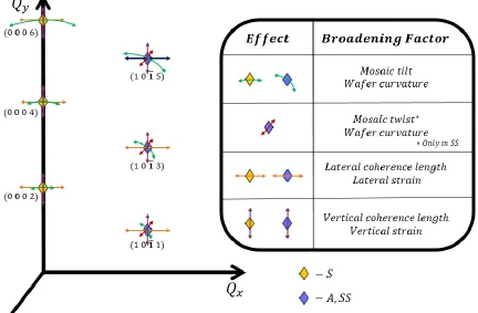
Figure 3.9. Schematic of an epitaxial layer, as described by the mosaic structural model. Four characteristic parameters are available through this model: lateral coherence length (LCL), vertical coherence length (VCL), mosaic tilt and mosaic twist. The model is equally applicable to bulk materials………...………58
Figure 3.10. Representation of reciprocal lattice broadening due to sample imperfections. The red line is directed out of the plane. Image adapted from Ref. 65………..………59
Figure 3.11. Induced biaxial strain for epitaxial film grown on dissimilar substrate. Lattice parameter differences between the film (𝑎𝑓) and substrate (𝑎𝑠) define tensile (𝑎𝑓< 𝑎𝑠) and compressive (𝑎𝑓 > 𝑎𝑠) strain in the plane of the film. Image adapted from Ref. 125………66
Figure 3.12. Broadening sources of symmetric and asymmetric reciprocal lattice points in III-nitride semiconductors. The combination of both a symmetric and asymmetric RSMs allow for strain and compositional gradients to be separated for correct lattice parameter assessment………..………..72
Figure 4.2. (0002) XRCs of differently polished AlN substrates, labeled in plot legend. Observations on XRC-FWHM and diffuse scatter magnitude are utilized to quantify crystal quality and wafer surface damage………....90
Figure 4.3. High-resolution (0002) RSMs for all CMP processed AlN wafers. Maps offer two characteristic diffraction features: the pole diffuse scatter and the CTR. In contrast to the 1 hr CMP sample, the diffuse scatter magnitude present in RSMs measured for the 3 hr and 6 hr processed wafers look comparable. Similarly, the CTR shape and extension in 𝑄𝑦 for the 3 hr and 6 hr CMP samples is identical, while the 1 hr CMP exhibits a more curved CTR, slightly
broadened in 𝑄𝑥………94
Figure 4.4. Areas of reciprocal space that are accessible using a conventional diffractometer. Shaded regions indicate the limits due to the beam blocking. The (101̅3) is positioned close to the semicircles, requiring a highly asymmetric geometry………...98
Figure 4.5. (101̅3) RSMs of differently polished AlN substrates. Unlike symmetric XRCs and RSMs, EAR RSMs do exhibit noticeable differences between the CMP treated surfaces. Metrics for subsurface damage quantification may be extracted from the diffuse scatter magnitude and the CTR extension………..100
Figure 4.6. Extracted triple-axis 𝜔-scans from (101̅3) RSMs for CMP processed AlN wafers. Measuring the FWTTM, the magnitude of the pole diffuse scatter could be quantified. Using this value as a metric, the 6 hr CMP processed wafer could be identified as the sample with the least amount of subsurface damage………...……….102
Figure 4.7. (101̅3) RSMs of the 1 hr and 6 hr CMP processed AlN wafers. The CTR extends uniformly in the 𝑄𝑦-direction, enabling a radial line scan to evaluate and quantify its diffracted intensity profile………..104
the 6 hr CMP processed AlN wafer may be identified as the least damaged surface, displaying the most intense CTR FWHHM value………...…….105
Figure 4.9. AFM images of differently polished FS GaN surfaces: a) mechanical polished, b) 15 min CMP, c) 30 min CMP and d) 60 min CMP. The mechanically polished and 15 min CMP samples exhibit readily visible damage features, such as deep scratches. The 30 min and 60 min CMP micrographs appear featureless and indistinguishable, indicating a potential threshold of the technique………...109
Figure 4.10. Field emission SEM images acquired for all processed FS GaN wafers. Results confirm observations from AFM micrographs. Both techniques resolve polishing-damage in the mechanically polished and 15 min CMP treated samples. However, like AFM imaging, the field emission SEM cannot distinguish between the 30 min and 60 min CMP processed surfaces………..111
Figure 4.11. Near band edge LT-PL spectra acquired for all processed (0001) FS GaN crystal surfaces. Two D°X emission lines are identified at 3.471 eV and 3.472 eV, with FWHM values of less than 200 μeV. The exciton lines are extremely narrow and do not exhibit peak position shifts, confirming the high optical quality of the FS GaN material………..112
Figure 4.12. On-axis XRCs recorded for processed FS GaN samples, measured about the (0002) reflection. The mechanically polished sample exhibited a comparatively broader XRC width and higher diffuse scatter intensity in contrast to CMP processed GaN crystals. The diffuse scatter intensity is not distinguishable between the CMP treated wafers.…………...115
Figure 4.14. (0002) RSMs recorded for the mechanically polished and 15 min CMP processed FS HVPE-GaN wafers. The mechanically polished sample exhibits an RSM populated with diffuse scatter halos about the RLP. In contrast, the 15 min CMP map has a substantially reduced amount of pole diffuse scatter and CTR visibility, which evidence an improved GaN crystal surface………...………..119
Figure 4.15. (0002) RSMs measured on 15 min, 30 min and 60 min CMP processed FS HVPE-GaN. Longer exposure to CMP processing resulted in less damage on the GaN crystal surface, as evidenced by the vast reduction in pole diffuse scatter intensity………….……..120
Figure 4.16. Extracted triple-axis 𝜔-scans from (0002) RSMs for CMP processed FS HVPE-GaN wafers. The pole diffuse scatter is difficult to quantify and compare among the 30 min and 60 min CMP samples due to the asymmetric line shape created by a misoriented bulk grain………..….121
Figure 4.17. (0004) RSMs recorded for all CMP processed FS GaN crystals. All maps exhibit intense CTRs, extended along the entire 𝑄𝑦 range of the measurement. The maps shows slight differences in diffuse scatter distributions between the 30 min and 60 min CMP treated samples due to the presence of secondary poles created by the the misoriented bulk grains………..122
Figure 4.18. CTR profiles taken from (0002) and (0004) RSMs for CMP processed FS GaN
crystals. The CTR elongation could not be quantified due to the asymmetric line shape of the
extracted 𝑄𝑦-scans……….123
Figure 4.19. (111̅4) RSMs of the 30 min and 60 min CMP processed FS GaN crystals. The maps show readily visible differences in diffuse scatter distributions, not accessible using symmetric measurements………...125
Figure 5.2. Wurtzite primitive unit cell and zinc blende non-primitive unit cell, denoting the stacking sequence of anions (filled circles) and cations (open circles) for each crystal structure. Image adapted from Ref. 207……….….131
Figure 5.3. Stacking sequences for intrinsic (𝐼1 and 𝐼2) and extrinsic (𝐸) BPSFs observed in wurtzite III-nitrides. Introduced sphalerite units are highlighted. Image taken from Ref. 207………..132
Figure 5.4. 5 x 5 μm2 AFM scan of m-plane (11̅00) AlN substrate surface free of gross polishing damage. The image shows monolayer steps of 2.7 ± 0.1 Å step height (one m-plane monolayer) and an RSM roughness of below 100 pm……….137
Figure 5.5. Symmetric (101̅0) XRCs of an m-plane AlN substrate, taken parallel and perpendicular to the [0001] direction. Differences in curve broadening and line shape reveal mosaic anisotropy due to the tilt and twist of the original [0001]-oriented AlN boule……138
Figure 5.6. Variation of the symmetric (101̅0) XRC-FWHM with azimuth angle for two m-plane AlN single crystal substrates. Data evidences the anisotropic shape of the reciprocal lattice point, attributed to the inherited mosaic tilt and twist of the original [0001]-oriented AlN crystal boule………...139
Figure 5.7. Symmetric (101̅0) RSMs of the m-plane AlN substrate, oriented (a) parallel and (b) perpendicular to the [0001] direction. Large mosaic broadening (𝑄𝑥 extension) is observed for the reflection recorded perpendicular to the [0001] direction, while no substantial broadening is seen for the measurement recorded parallel to this direction………142
Figure 5.8. 5 x 5 μm AFM images of (11̅00) homoepitaxial AlN films grown at three different
temperatures. A decrease in surface roughness with increasing growth temperature is observed……….145
Figure 5.9. Symmetric (101̅0) XRC of m-plane AlN homoepitaxial films grown at 1150°C
Figure 5.10. W-H plots of (ℎ0ℎ̅0) XRCs for three m-plane AlN homoepitaxial films grown at different MOCVD growth temperatures………149
Figure 5.11. Symmetric (101̅0) XRCs measured perpendicular to the [0001] direction. In contrast to the substrate, the films exhibit minimal variations in curve broadening and line shape with in-plane sample orientation………..……151
Figure 5.12. Symmetric (101̅0) 2𝜃-𝜔 line scans for m-plane AlN homoepitaxial films grown at five different growth temperatures. The intensity of Pendellösung fringes is seen to decrease as the film growth temperature was increased, indicative of a less abrupt electron density difference between the film and substrate due to a reduction in impurity incorporation……152
Figure 5.13. RSMs of the (101̅0) reflection for them-plane AlN homoepitaxial films grown at a) 1150°C and b) 1350°C. A reduction in the pole diffuse scatter and CTR length extension is observed for the higher temperature film. No BPSF-related streaks are observed……….155
Figure 5.14. RSMs of the (101̅0) reflection for the m-plane AlN homoepitaxial films grown
at a) 1350°C and b) 1550°C. A further reduction in the pole diffuse scatter and CTR extension is observed for the highest temperature film. As in Figure 5.13, BPSF-related streaks are not resolved………..156
Figure 5.15. RSMs of the (202̅0) reflections for a) 1150°C and b) 1550°C films. Intensity colorscale is the same as in Figure 5.14. As in (101̅0) maps, the higher temperature film exhibits a reduction in pole diffuse scatter intensity and a more defined CTR. According to the invisibility criteria, characteristic diffuse scatter corresponding to BPSFs should be observed in RSMs recorded about the (101̅0) and (202̅0) reflections, but not resolved in (303̅0) maps………..……….157
Figure 5.17. TEM images of homoepitaxial m-plane AlN two-layer stack grown at 1450°C and 1350°C, respectively. White horizontal arrows indicate the start of the 1450°C (lower) and 1350°C (upper) films. Images show no visible interface or defect contrast. Minor streaks (yellow arrow) and thickness contrast (green arrow) are seen due to sample preparation artifacts………...160
Figure 6.1. Symmetric (0002) 2𝜃-𝜔 scans of four different AlxGa1-xN films grown on AlN single crystals. The appearance of Pendellösung fringes evidences smooth interfaces and high crystallinity of the alloy films……….………164
Figure 6.2. 2𝜃-𝜔 radial scans of metrically equivalent GI (101̅5) and GE (1̅015) reflections.
The difference in Bragg peak positions between the AlGaN epilayer and AlN substrate are extracted and reported as ∆𝜔(101̅5) and ∆𝜔(1̅015). Combined with the ∆𝜔(0002), these values are used to calculate AlGaN alloy composition and relaxation degree………...167
Figure 6.3. (0002) RSM recorded for an AlGaN alloy epilayer (Sample A) deposited on an AlN substrate. The use of either the AlGaN or AlN RLP for beam path alignment (𝜔-orientation) does not jeopardize the accessibility of both the epilayer and substrate in a single line scan………..169
Figure 6.4. Asymmetric RSM recorded for an AlGaN alloy epilayer (Sample A). In contrast to the symmetric scan, the beam path alignment can affect the accessibility of both the epilayer and substrate RLPs in a single line scan……….170
Figure 7.1. Lattice mismatch and compressive strain of AlxGa1-xN alloys on AlN………..173
Figure 7.2. Illustration of crystallographic tilting by heteroepitaxial layer. The lattice cells of the layer adjacent to the offcut substrate change in c lattice parameter at the edges of the substrate steps. Image taken from Ref. 260……….174
Figure 7.4. Predicted Nagai tilt trend of AlGaN epilayers deposited on AlN substrates with high offcut surfaces………176
Figure 7.5. AlGaN tilt trend with respect to AlN offcut magnitude, as measured from HRXRD methods. Linear trend coincides with pseudomorphic alloy films (Nagai tilt model). However, knowledge on the AlGaN film alloy composition and strain state is necessary for tilt results to become conclusive……….178
Figure 7.6. (0002) radial scans measured at different incident X-ray beam orientations with respect to the sample surface………. …179
Figure 7.7. Symmetric (0002) RSMs taken for an AlGaN alloy film of nominal 𝑥𝐴𝑙=0.80 composition deposited on AlN. The RSMs are oriented a) perpendicular to the substrate offcut, b) parallel to the [101̅0] direction and c) parallel to the offcut direction. The AlGaN RLP exhibits slight shifts about the 𝑄𝑥-axis due to the epilayer lattice tilt with respect to the substrate……….180
Figure 7.8. Symmetric (0002) and asymmetric (101̅5) RSMs taken for an AlGaN alloy film of nominal 𝑥𝐴𝑙=0.70 composition. Both RSMs were taken parallel to the substrate offcut. As observed for the sample presented in Figure 7.7, the AlGaN RLP exhibits slight a shift about the 𝑄𝑥-axis in the asymmetric RSM due to the epilayer lattice tilt………181
Figure 7.9. RSMs for the a) (0002) and b)(101̅5) reflections of a nominally 60% Al AlGaN alloy film. The RSMs were taken parallel to the [101̅0] direction, which is oriented parallel to the substrate offcut direction. The AlGaN RLP exhibits a large shift, moving completely away from the 𝑄𝑥-coordinate of the AlN RLP center. Extracted AlGaN RLP positions result in a calculated alloy composition of 𝑥𝐴𝑙=0.70………...182
fully strained to the AlN substrate, and has an alloy composition of
𝑥𝐴𝑙=0.60……….…………184
Figure 7.11. (0002) RSMs taken a) perpendicular to the offcut direction and b) parallel to the offcut direction. Measurements reveal the AlGaN epilayer is tilted with respect to the substrate. A different shape in the AlGaN RLP is observed………..185
Figure 8.1. Theoretical calculation of TDD dislocation densities necessary to fully relax AlGaN alloys grown on AlN substrates……….192
CHAPTER 1: INTRODUCTION
1.1. Motivation
Group III-nitrides are among the most fascinating and technologically relevant materials systems of our time. Comprised of AlN, GaN, InN and their alloys, this remarkable family of semiconductors presently constitutes the main component of several modern electronic and optoelectronic devices, such as high-power, high frequency transistors, light emitting diodes (LEDs) and laser diodes (LDs) [1, 2]. Over the last ten years, III-nitrides have been intensely pursued in academic, government and industrial settings in an effort to further their applicability for novel semiconductor applications. Advances in every developmental stage have resulted in an extensive body of well-documented studies, observations, innovative solutions and technological breakthroughs that have contributed to the continuous understanding and usage of these important materials [1-10]. As progress and interest continue to increase, III-nitrides are expected to yield more revolutionizing technologies that will soon transform the medical, power, communications and solid-state lightning industries all over the world [11, 12].
The recent availability of GaN and AlN single crystals has allowed the nitride research community to explore the opportunities offered by homoepitaxial crystal growth. While some remarkable results have already evidenced the benefits of using native nitride substrates, there are unfortunate setbacks preventing their mass marketability and utilization. Indeed, the demand for native nitride crystals is comparable to other commercialized substrates. But, native substrates suffer from much higher growth-related expenses and manufacturing costs. Furthermore, there is a substantial lack of mastery and knowledge in adequate processes for wafer preparation and subsequent film deposition, requiring more careful experimentation and detailed observations.
Since it becomes necessary to use non-destructive, rapid and accurate techniques that can assess and monitor the evolution of microstructural features in single crystalline substrates and homoepitaxial nitride films, characterization tools like X-ray diffraction (XRD) are viewed as ideal for the task. XRD methods are proven to be informative, reliable, precise and widely versatile, becoming a standard and practical aid for quality control to the III-nitride semiconductor engineer. This chapter serves to introduce the historical aspects that have motivated the progress and future applications of advanced III-nitride materials, with special emphasis on the need to further improve structural quality assessment via novel XRD metrology.
1.2. General Properties of III-Nitride Semiconductors
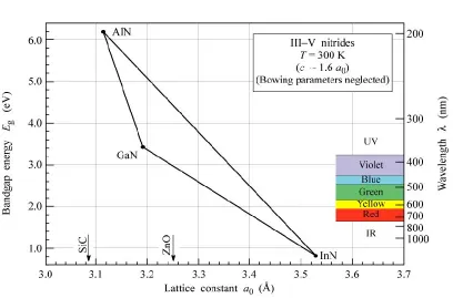
corresponding to a wavelength range that covers the infrared, visible and ultraviolet spectral regions [13, 14]. The III-nitride 𝐸𝑔 spectrum proves advantageous when multipurpose optoelectronic devices are considered, where the emission and absorption wavelength ranges can be tuned using binary, ternary and quarternary III-nitride alloy combinations. Figure 1.1. depicts a comparison of the 𝐸𝑔 as a function of the in-plane lattice parameter [14].
Figure 1.1. Bandgap energy versus the a lattice parameter of III-V nitride binary compounds (wurtzite) at room temperature. Image taken from Ref. [14]
Regarding their structural properties, III-nitride compounds can be found in rocksalt, zinc blende and wurtzite crystal forms. The work presented in this dissertation focuses on the hexagonal wurtzite structure, which is the most thermodynamically stable [5, 17, 18]. This structure is a type of hexagonal close-packed (HCP) lattice with dimensions reported as lattice constants 𝑎 and 𝑐, which describe the edge length of the basal plane hexagon length and cell height, respectively [5, 19]. Belonging to the P63mc space group (Hermann-Mauguin notation), the wurtzite unit cell contains III-metal (Al3+,Ga3+ or In3+) cations and N3- anions, arranged into two interpenetrating HCP sublattices, each with one type of atom and offset 5c
As depicted in Figure 1.2a, the N atoms form the main HCP arrangement, each coordinated by four III-metal atoms. Respectively, each III-metal atom is surrounded by four N atoms, leading to an overall compound coordination of 4:4 [5, 22]. As there are two tetrahedral sites available for every N atom, III-metal atoms are said to occupy half of the tetrahedral sites [5, 19, 22, 23]. If the unit cell is projected along the c-axis, as shown in Figure 1.2b, it becomes evident that the unit cell lacks true inversion symmetry. The non-centrosymmetry of the structure and ionic nature of the III-metal and N bonds gives rise to an intrinsic crystal polarization. The crystal polarity is determined by the arrangement of III-metal cations on tetrahedral sites either above or below a height 3c
Figure 1.2. Unit cell representation of the wurtzite crystal structure for III-nitride compounds, depicting both a and c lattice parameters (left). In the partial unit cell (right), the atomic arrangement that gives rise to non-centrosymmetry and internal crystal polarization along the c-axis is depicted. P is the polarization vector, pointing from the cation (filled circles) to the anion (unfilled circles).
Figure 1.3. Crystallographic orientations of the wurtzite structure. The polar (0001) plane is commonly referred to as the c-plane, while the non-polar (112̅0) and (101̅0) are the a-plane and m-plane, respectively.
In a useful manner, the unit cell can also be described as a sequence of alternating close-packed (0001) planes of III-metal and N pairs [5]. For the hexagonal wurtzite structure, the polytypic stacking sequence along the c-axis is …ABABABAB…, where each letter identifies bilayers containing one type of atom either in the main HCP array or tetrahedral voids, respectively [5, 26]. This stacking order designation is necessary for the description of partial lattice displacements named stacking faults, which will be discussed further in Chapter 5.
1.3. Historical Perspective: The Need for High Crystal Quality
technologies that were limited by other well-established material systems. An exemplary case can be found in the history of GaN-based blue-light LEDs.
By the 1960s, Radio Corporation of America (or RCA) was a major electronics company heavily pursuing a viable replacement to the cathode-tube color television sets [30, 31]. LEDs were a formidable option to substitute the present outdated technology, since red and green LEDs had already been demonstrated using GaAs and GaP compound semiconductors [31]. Still, the achievement of LED television screens required one additional, critical piece: the blue-light emitting LED [31]. Not only for televisions, blue LEDs were strongly pursued to further replace incandescent white light bulbs and transform lighting technologies into more efficient, LED illuminating devices. But, the numerous failed efforts and attempts towards their generation proved this to be a great challenge, pinpointed to be potentially solved if GaN-based layers were implemented in LED microelectronic structures instead of ZnSe or SiC, which possess high indirect bandgaps [32, 33]. This idea was inspired by early optical investigations done at Philips Research laboratories, where Hermann Georg Grimmeiss and Hein Koelmans were able to obtain efficient photoluminescence from micro-crystalline and GaN powders, identifying an attractive direct wide bandgap of 3.5 eV [33-35]. Hence, many laboratories began to search for synthesis routes that would produce high quality GaN thin films.
chloride in a growth chamber [37, 38]. With this method, Maruska was able to synthesize for the first time single-crystal GaN epilayers on mechanically-polished sapphire substrates [37, 38].
Soon after, undoped and doped GaN products were optically characterized by Dr. Jacques Pankove, who reported for the first time the electroluminescence of GaN [42, 43]. As further research continued, it was evident that the next big challenge would be achieving p-type doping in GaN. Partially remediated by injecting holes into n-type GaN by means of a metal-insulator-semiconductor (MIS) barrier, Pankove and Edward Miller were able to construct structures that led to the first bluish-green LED in 1971 [15, 43]. But in order to achieve high-brightness blue light emission, p-type GaN epilayers would need to be developed for GaN-based p-n junctions, the building blocks of LEDs [33, 44, 45].
The realization of n- and p-type doped GaN with high structural quality, smooth surfaces and controllable electrical conductivity was made possible through the extensive works of Shuji Nakamura, Isamu Akasaki and Hiroshi Amano [44]. At the time working at Nagoya University in Japan, Akasaki predicted the GaN-based p-n junction would only be possible if doped layers could be produced at the same quality level as small, high-quality microcrystals he often observed in single-crystal GaN grown by molecular beam epitaxy (MBE) [36]. However, while weighing the disadvantages of many methods already explored for GaN growth, it seemed clear that metal-organic vapor phase epitaxy (MOVPE) would be the ideal technique to grow highly crystalline nitride films. Unfortunately, the initial growth attempts failed dramatically, attributed to the difference in material parameters with sapphire (substrate) that led to cracked, highly defective GaN [44]. Therefore, any continuation to MOVPE GaN synthesis would require a clever solution that could alleviate the problems arising at the film and substrate interface [44].
layer [15, 44]. Thorough characterization demonstrated that the insertion of this very thin layer (30 nm) of AlN nucleated on sapphire led to epitaxial films of device grade, with appreciably improved optical, crystal and electrical quality and much lower background impurities [33]. Independently, Nakamura was able to grow high-quality GaN, using a similar growth strategy that employed a thin GaN layer instead of AlN [33, 46, 47]. But while problems regarding quality were resolved, the ability to conduct p-type doping remained.
The adaptation of LT-buffer layers for GaN allowed for early doping experiments using Zn and Mg to be revisited. Through routine cathodoluminescence (CL) studies, Akasaki and Amano were astounded to see the light emitted by Zn-doped GaN would became highly intense when performing this characterization [33, 44, 48]. While puzzling, this result was evidence of improved p-doping (activated Zn acceptors) through exposure to low-energy electron beams, although p-type conductivity was not shown by the Zn:GaN films. Akasaki realized that using Mg as the dopant would be an easier way towards effective p-type doping, since it was a shallower acceptor. In 1989, the first p-type doping of GaN was finally achieved, advancing a huge step towards constructing GaN p-n junctions [33, 44, 49, 50].
applications in a large range of scientific fields. This was a direct result of the necessary improvement of structural and optical characteristics in III-nitride heteroepitaxial materials, without which their potential for electronic and optoelectronic device applications would have remained unexplored. It was the critical advancements made through MBE and MOVPE growth methods that allowed for III-nitride material capabilities to be experimentally explored and further understood, yielding their technological relevance among other III-V semiconductors [1].
Nowadays, III-nitride-based LEDs and LDs are the dominant technologies for general lightning technologies, back-illuminated liquid crystal displays, high-density optical data storage, among others. Continuous commercial and scientific activity have motivated new research and development, with particular advances that have forecasted future desirable applications to be pursued and potentially realized in the next decade. For example, there is practical interest in accomplishing UV/DUV LEDs and LDs for biomedicine, such as sterilization and water purification, since UV light destroys the DNA of bacteria, viruses and microorganisms [33, 55]. Likewise, III-nitrides are envisioned to produce hybrid photoelectrochemical cells for renewable solar fuel generation [2]. Yet, to be targeted, all these modern technologies will require reproducible materials of even higher quality that can facilitate properly tailored structures required for device design and functionality [2]. For this, some solutions are presently being investigated, such as the growth of III-nitride structures on native substrate materials.
1.4. III-Nitride Epitaxial Structures for Modern Devices
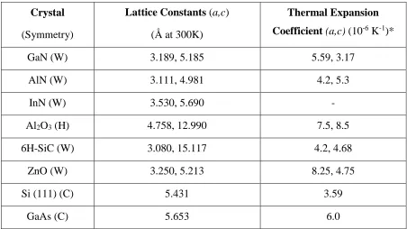
commonly used substrates for III-nitride epitaxy. As reported, none of these crystal substrates are closely matched in lattice parameters or thermal expansion coefficient to any of the III-nitride binary compounds. Specific crystal orientations allow desirable epitaxial relationships in otherwise highly mismatched systems, such as [112̅0] GaN on [112̅0] SiC (∆𝑎
𝑎 = 3.5 %) and [011̅0] GaN on [112̅0] sapphire (∆𝑎
Table 1.1. Properties of most commonly used substrates for III-nitride epitaxial growth. The thermal expansion coefficient values are reported for the common MBE growth temperature of 800°C [59].
Crystal
(Symmetry)
Lattice Constants (a,c) (Å at 300K)
Thermal Expansion
Coefficient (a,c)(10-6 K-1)*
GaN (W) 3.189, 5.185 5.59, 3.17
AlN (W) 3.111, 4.981 4.2, 5.3
InN (W) 3.530, 5.690 -
Al2O3 (H) 4.758, 12.990 7.5, 8.5
6H-SiC (W) 3.080, 15.117 4.2, 4.68
ZnO (W) 3.250, 5.213 8.25, 4.75
Si (111) (C) 5.431 3.59
GaAs (C) 5.653 6.0
W- Wurtzite, H- Hexagonal and C- Cubic
high-electron mobility transistors (HEMTs) and Schottky barrier diodes (SBDs). For this, III-nitrides must evolve from their current heteroepitaxial scenario, reaching a comparable epitaxial setting as other better-matched III-V heterosystems, such as (In, Ga, Al)As/InP and AlGaAs/GaAs [60].
1.5. XRD Characterization for Future III-Nitride Materials
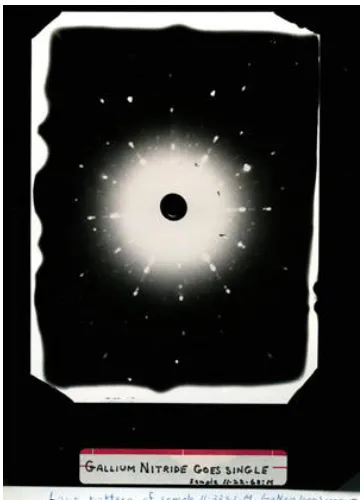
Early X-ray experiments on III-nitride semiconductor materials relied on old diffraction techniques, such as the Laue method. In fact, during the developmental stages of single crystal GaN, Maruska recorded Laue patterns of his GaN films, evidencing their high crystallinity and structural perfection (Figure 1.4). Since then, outdated diffraction methods have been replaced by more powerful modern techniques that can provide further information on key layer parameters that are of critical interest to the semiconductor engineer [63]. These are now readily accessed by means of high-resolution X-ray diffraction (HRXRD) measurements.
By the 1980s, HRXRD became a well-established in-line routine metrology in most compound semiconductor fabrication laboratories [64]. Nowadays, techniques such as double-crystal rocking curves and triple-crystal diffraction have become essential tools for quick and non-destructive characterization, applicable to a wide range of materials and epitaxial structures, including the III-nitride semiconductors [63]. Particularly for stepped processing, HRXRD is essential, since measurements are rapid, representative and precise, without requiring extensive sample preparation schemes that often lead to its partial or total destruction [65]. Wafer and film metrologies available through HRXRD experiments include strain, thickness, phase, composition, dislocation density, surface and interfacial roughness, bowing, porosity, texture and crystallinity [64, 65]. Therefore, the employment of adequate HRXRD techniques for the structural assessment and quality control of bulk crystals, single epitaxial films and multilayered III-nitride heterostructures is extremely beneficial.
1.6. Dissertation Overview
The main aim of this research is to present a comprehensive study on the HRXRD characterization of epitaxial products obtained using native single crystalline substrates. The influence of substrate conditions and MOCVD growth parameters on the resulting film characteristics have been investigated, with the objective of extending common measurement techniques to novel practices that can better serve the analysis of this new class of III-nitride materials.
As an introduction, Chapter 2 begins with a brief overview of general concepts used in X-ray diffraction, such as wave scattering physics and the kinematical and dynamical diffraction theories. Chapter 3 presents modern HRXRD techniques, where diffraction theories are related to common instrumentation, measurement types and interpretation models relevant to semiconductor metrology.
Experimental data and results begin with Chapter 4, where the effect of subsurface damage from polishing procedures on HRXRD measurements is investigated. The use of specific techniques to qualitatively and quantitatively assess the presence of polishing-induced damage in differently processed single crystalline AlN and GaN substrates is explored and discussed. In Chapter 5, HRXRD techniques for the structural investigation of homoepitaxial AlN non-polar m-plane films are presented. The effect of MOCVD growth temperature on the surface quality and overall crystallinity of the non-polar epitaxial films is explained.
In Chapter 6, observations on the employment of routine HRXRD methods for the assessment of strain and composition in AlGaN alloys deposited on AlN single crystals is discussed.
Chapter 7 extends this discussion to crystallographically tilted Al-rich AlGaN alloys grown on differently offcut AlN substrates. The degree of tilt magnitude with substrate offcut is followed and related to limitations in strain and alloy composition determination.
CHAPTER 2: X-RAY DIFFRACTION THEORY
2.1. Introduction
At the end of the 19th century, German physicist Wilhem Conrad Röntgen became interested in investigating the effects of electrical current flowing through gases in low pressure glass tubes [66, 67]. Using a Hittorf-Crookes tube setup, Röntgen noticed that the emitted rays from the operating tube had produced an unexpected fluorescent light on a nearby piece of cardboard painted with barium platinocyanide [66, 68]. Puzzled by this observation, Rontgen repeated his experiment with an intentionally covered tube, using heavy black cardboard to block the discharge glow caused by electrons striking the tube glass envelope [66-68]. Yet, after repeating his experiment multiple times, he continued to see fluorescent light emitted from the barium platinocyanide screen placed a good distance away from the tube [68, 69]. Convinced this effect was the result of electrons striking the glass walls of the tube, he theorized that a new kind of unknown radiation was repeatedly being produced during his experiments, which he termed “X-rays” [66-69].
framework for crystal diffraction theory that became the basis for its practical experimental use in crystallography studies [70-74].
It is now well understood that X-rays are highly energetic electromagnetic waves of very short wavelengths, on the order of crystal lattice spacings. It is the interaction of X-rays with the electrons surrounding atoms regularly arrayed in crystal planes that gives rise to the physical phenomenon of diffraction. Since the intensity and pattern produced by diffracted X-rays depends on both the type and spatial arrangement of atoms in a crystal lattice, the analysis of XRD data is an ideal technique to investigate the structural properties of crystalline solids. In this chapter, a brief introduction to concepts utilized in diffraction physics is provided. The discussion offered is only meant to provide a basic understanding of the scattering of X-rays and the phenomena of diffraction from crystalline structures.
2.2. Scattering of X-rays
2.2.1. Kinematical Theory of Diffraction
To fully understand scattering from a crystalline structure, it is often useful to begin with the simplest case, where a scattering center is just a single free electron. When X-rays interact with electrons, the resulting scattering process may be categorized as either inelastic, elastic, coherent and/or incoherent [75-77]. Inelastic scattering defines processes in which the energy of the incident X-ray waves are transferred to the electron, such as Compton scattering and photon ionization [75, 76]. In contrast, elastic scattering involves no energy or momentum exchange. The electric field of the incident X-ray wave perturbs the electron and its acceleration, causing it behave like an oscillating electric dipole. Continuously accelerating and decelerating during its motion, the electron reemits new electromagnetic waves of the same wavelength and frequency as the incident wave [78]. The coherence of scattering refers to whether there are specific phase relationships between the reemitted electromagnetic waves that allows these to interfere constructively and destructively [77]. If there is no definitive phase relationship between the scattered X-ray waves, the event is categorized as incoherent; there is no interference and the resulting intensity is the sum of the intensities of the individual waves [77]. Conversely, in a coherent scattering event, the waves interfere and the total scattering intensity is the square of the sum of the X-ray wave amplitudes [77]. Thus, it is the coherent scattering of X-rays that contains structural information [77].
Coherently scattered X-rays from a free electron may travel a distance R towards a point of observation, where the observed scattering intensity can be expressed as:
𝐼 = 𝐼0 𝑃∗𝑟𝑒2
𝑅2 ,
The ratio 𝐼
𝐼0 is often referred to as the electron scattering factor. Similarly, an atomic scattering
factor, f, can be defined by coherently adding the scattering response of all electrons in an atom. This can be readily done by multiplying the free electron scattering factor by the atomic number, Z. However, this approach is only correct if all electrons are concentrated in a particular point in space and the scattering is in the forward direction, described by scattering angle of zero (nearly in-phase scattering) [64]. Since electrons are distributed within an atomic electron cloud, the scattered wave relationships must accounted for in order to properly describe coherent scattering intensity from an atom. One must add the scattered waves with regards to phase, since non-zero values of the scattering angle produce phase variations [64]. Consider an electron at a position vector 𝒓𝒊 with respect to the atomic nucleus (or any arbitrarily assigned origin). The scattering response from this electron will produce an optical path difference of (𝒌 − 𝒌𝟎) ∙ 𝒓𝒊, where 𝒌𝟎 and 𝒌 are the wave vectors that describe the incident and scattered X-ray waves, respectively [78]. Then, scattered waves will be out of phase with those scattered at the atomic nucleus by a factor 𝑒𝑥 𝑝 (2𝜋𝑖
𝜆 (𝒌 − 𝒌𝟎) ∙ 𝒓𝒊) [64]. Knowing these phase relationships, the total atomic scattering factor for an atom containing Z electrons can be expressed as:
𝑓 = ∑ 𝐼 𝐼0exp (
2𝜋𝑖
𝜆 (𝒌 − 𝒌𝟎∙ 𝒓𝒊) 𝑍
𝑖=0
(2.2)
It proves convenient to define the difference between the incoming and outgoing wave vectors as the scattering vector, 𝑸. Figure 2.1 serves to illustrate these vector relationships, where the magnitude of both 𝒌𝟎 and 𝒌𝒉 is 1
𝜆. The magnitude of 𝑸 is written as: |𝑸| =2 sin 2𝜃
𝜆 ,
where 2𝜃 is the scattering angle [64]. Aside for simplifying mathematical expressions, defining the scattering vector is important to illustrate X-ray scattering in reciprocal space, which will be discussed in further sections.
Figure 2.1. Schematic of the scattering vector, 𝑸, and its relationship to the incident (𝒌𝟎) and scattered (𝒌𝒉) wave vectors.
Electrons surrounding the atomic nucleus are not usually assigned fixed points, but rather described by means of a probability density function. Denoted as 𝜌(𝑟), this probability function is a function of the distance r away from the nucleus [78]. Using the electron density, a more familiar expression for the atomic scattering factor can be obtained:
In the same manner that atomic scattering factors are calculated by coherently adding the scattering response of electrons in an atom, the total scattering from a unit cell may be obtained by coherently adding the scattering contributions of all comprising atoms. As before, it is important to account for phase differences, which arise from the relationships between the scattering intensity and atomic positions. [78]. Doing so, the total scattering power of 𝑁 number of atoms within a unit cell may be written as:
𝐹(𝑄) = ∑ 𝑓𝑗(𝑄)exp (2𝜋𝑖𝑸 ∙ 𝒓𝒋) 𝑁
𝑗=1
(2.5)
where 𝒓𝒋 is the position vector of the 𝑗th atom. This expression is known as the structure factor for a unit cell. As will be seen, the experimentally measured diffracted intensity is proportional to the square of the structure factor, |𝐹(𝑄)|2, which allows the determination of contents within unit cells, and hence, the identification of crystalline materials.
Finally, the scattering amplitude of the entire crystal is obtained by adding the scattering response from all unit cells within the crystal. For this, a vector 𝑻𝒌 is defined, which describes the position of the 𝑘th unit cell. Then, the total scattering amplitude is written as:
𝐴(𝑄) = [∑ 𝑓𝑗(𝑄)𝑒𝑥𝑝(2𝜋𝑖𝑸 ∙ 𝒓𝒋) 𝑗
] [∑ 𝑒𝑥𝑝(2𝜋𝑖𝑸 ∙ 𝑻𝒌 𝑘
)] = 𝐹𝑘(𝑄)𝐽(𝑄)
(2.6)
where 𝐹𝑘(𝑄) is the structure factor for the 𝑘th unit cell, and 𝐽(𝑄) is the interference function [64]. To evaluate the interference function, it proves helpful to describe the crystal as a parallelepiped, whose dimensions are conveniently defined with respect to the unit cell basis vectors 𝒂, 𝒃, and 𝒄 [64]. Letting 𝑁𝑖 denote the number of unit cells in each side of the parallelepiped, then 𝐽(𝑄) can be expressed as:
𝐽(𝑄) = ∑ 𝑒𝑥𝑝 (2𝜋𝑖𝑁1𝒂 ∙ 𝑸 𝑁1
𝑁1=1
) ∑ 𝑒𝑥𝑝(2𝜋𝑖𝑁2𝒃 ∙ 𝑸) 𝑁2
𝑁2=1
∑ 𝑒𝑥𝑝 𝑁3
𝑁3=1
(2𝜋𝑖 𝑁3𝒄 ∙ 𝑸)
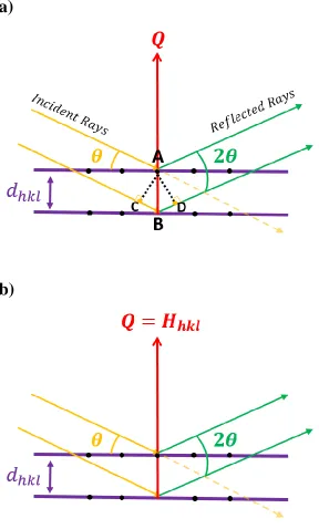
where specific values must be assumed by the scattering vector in order for 𝐽(𝑄) ≠ 0 [64]. In other words, there are particular geometrical conditions that must be satisfied for constructive interference of scattered X-ray waves to occur. If so, the resulting diffracted intensity may be expressed as 𝐼 = 𝐹2𝐽2. The necessary angular relationships between the atomic planes in a crystal and the incident and scattered X-ray waves are well represented by means of Bragg’s law.
2.2.1.1. Bragg’s Law and Diffraction
𝐶𝐵 = 𝐵𝐷 = 𝑑ℎ𝑘𝑙sin 𝜃 (2.8) Therefore, constructive interference occurs only when the path difference between the waves, 2𝑑ℎ𝑘𝑙sin 𝜃, is an integer number of the wavelengths, written formally as:
𝑛𝜆 = 2𝑑ℎ𝑘𝑙sin 𝜃, (2.9)
which is Bragg’s law [80] .
Figure 2.2. Constructive interference of reflected waves by successive atomic planes in a rectangular crystal. If the reflected rays are to continue to travel adjacent and parallel to each other, the incident ray on point B must travel an extra distance that is a multiple of the wavelength. Therefore, 𝑛𝜆 = 𝐶𝐵 + 𝐵𝐷 = 2𝑑ℎ𝑘𝑙sin 𝜃, formally known as Bragg’s law.
angle at which maximum diffracted intensity can be achieved, commonly referred to as the Bragg angle. There is no additional information on the angular range for the total scattering process or of the spread of intensities, which provide relevant information regarding the crystal structure [64].
2.2.1.2. Reciprocal Lattice and Scattering Vector
In order to understand experimental observations, such as the ranges of diffracted intensity and the shape of diffraction peaks, a more extensive and generalized concept must be introduced: the reciprocal lattice. As will be shown, explaining diffraction within the reciprocal lattice space proves to be a crucial interpretation tool, since it allows non-ideal situations to be considered and hence, aids the identification of observable diffraction features beyond a recognizable diffraction maximum.
The reciprocal lattice is a useful mathematical construct based on the real space dimensions of the crystal, where each lattice point is associated with a particular set of crystal planes. Reciprocal lattice points can be described by means of the reciprocal lattice vector, written as:
𝑯𝒉𝒌𝒍= ℎ𝒂∗+ 𝑘𝒃∗+ 𝑙𝒄∗, (2.10)
where 𝒂∗, 𝒃∗ and 𝒄∗ are the reciprocal space axes. These are related to the real space axes 𝒂, 𝒃 and 𝒄 by the following relationships:
𝒂∗ = 𝒃 × 𝒄 𝒂 ∙ [𝒃 × 𝒄]
(2.11a)
𝒃∗ = 𝒄 × 𝒂 𝒃 ∙ [𝒄 × 𝒂]
(2.11b)
𝒄∗ = 𝒂 × 𝒃 𝒄 ∙ [𝒂 × 𝒃]
crystal planes. Therefore, the normal to these planes corresponds to the reciprocal space vector [64]. As defined, the reciprocal lattice can be visualized to be attached to the real crystal lattice. Directions in both the real crystal lattice and reciprocal lattice are kept the same; if the crystal orientation is changed with respect to an incident beam, the reciprocal lattice orientation is changed as well. However, as its name suggests, the reciprocal lattice dimensions are in reciprocal length, where |𝑯𝒉𝒌𝒍| = 1
𝑑ℎ𝑘𝑙. As a result, any changes in the real crystal lattice that
alter the dimensions of interplanar d-spacings will consequently affect the position of reciprocal lattice points [65].
a)
b)
2.2.1.3. Ewald Sphere of Reflection
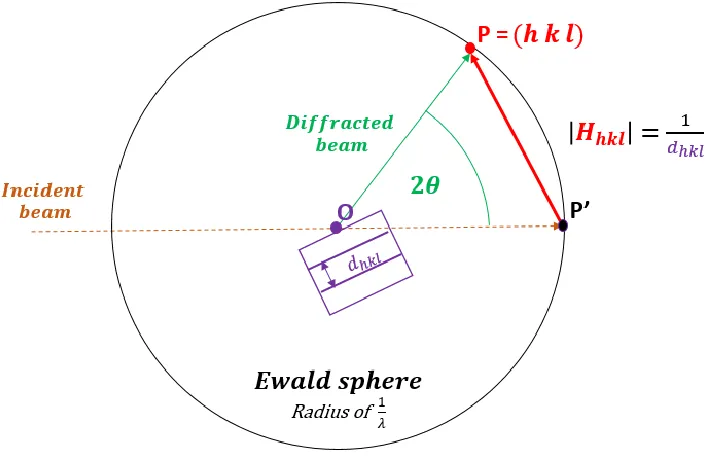
To illustrate the dependence of crystal orientation to the generation of diffraction, the Ewald sphere of reflection is often introduced, where the relationships between all components of the diffraction experiment are presented in a simple and useful manner. This sphere is usually represented in a two-dimensional reciprocal lattice, drawn as a circle of radius 1
Figure 2.4. Schematic of the Ewald sphere construction in reciprocal space. The sphere has a radius of 1
𝜆. The origin of both the real crystal lattice and reciprocal lattice is set at point 𝑂. The vector 𝑷′𝑷 corresponds to the reciprocal lattice vector 𝑯𝒉𝒌𝒍. When the set of (ℎ 𝑘 𝑙) crystal planes are in reflecting position (Bragg’s condition), 𝑃 lies on the surface of the Ewald sphere. As such, 𝑷′𝑷 = 𝑯𝒉𝒌𝒍= 𝑸, where 𝑸 is the scattering vector. The diffracted beam vector, 𝑶𝑷, is emitted towards a film plane or detector, where diffraction is recorded.
2.2.1.4. Diffraction from Real Crystals
[64]. Analogous to Laue and Bragg interpretation for diffraction, the Ewald sphere construction does specify a geometrical condition in reciprocal space for maximum diffraction: the intersection of the edge of the sphere with a reciprocal lattice point. But, in order to explain experimentally observed features that are not exactly at diffraction maxima (non-ideal situations), a more generalized treatment for the geometry of diffraction must be explored. For a single unit cell, Equation 2.5 can be used to describe the total scattering amplitude in the direction of (𝒌𝟎+ 𝑯𝒉𝒌𝒍). The structure factor takes the form:
𝐹(𝒈) = ∑ 𝑓𝑗(𝑯𝒉𝒌𝒍)exp (−2𝜋𝑖 𝑯𝒉𝒌𝒍∙ 𝒓𝒋) 𝑗
(2.12)
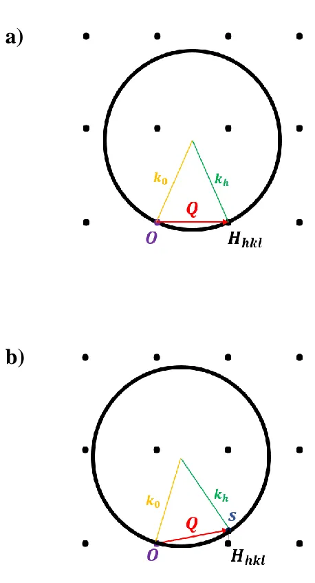
where 𝑯𝒉𝒌𝒍 is a vector in reciprocal space corresponding to (ℎ 𝑘 𝑙) planes and 𝒓𝒋 is the position vector of the jth atom in the unit cell. Again, this equation represents the scattering contributions of all atoms within the unit cell, coherently added in the direction (𝒌𝟎+ 𝑯𝒉𝒌𝒍). When two unit cells separated by 𝒓𝒋 are considered, the phase difference between the scattered X-ray waves at each unit cell is described as −2𝜋(𝑸 ∙ 𝒓𝒋), where 𝑸 is the scattering vector. As stated, when the crystal is at an exact Bragg position, 𝑸 = 𝑯𝒉𝒌𝒍. However, if such conditions are only partially satisfied, i.e. crystal is slightly deviated from the exact Bragg position, then 𝑸 ≠ 𝑯𝒉𝒌𝒍 (Figure 2.5). In order to describe diffracted intensities in such scenarios, the scattering vector can be expressed as:
𝑸 = 𝑯𝒉𝒌𝒍+ 𝒔, (2.13)
a)
b)
Experimentally observed intensities may be calculated by means of the deviation vector 𝒔 and the interference function, introduced in Section 2.2.1. Imagine diffraction occurring from a thin, perfect crystal, described as a parallelepiped of sides 𝑁1𝒂, 𝑁2𝒃 and 𝑁3𝒃. The interference function must be rewritten as a function of 𝑸 = 𝑯𝒉𝒌𝒍+ 𝒔:
𝒂 ∙ 𝑸 = 𝒂 ∙ 𝑯𝒉𝒌𝒍+ 𝒂 ∙ 𝒔 = ℎ + 𝑁1𝑠1 (2.14a) 𝒃 ∙ 𝑸 = 𝒃 ∙ 𝑯𝒉𝒌𝒍+ 𝒃 ∙ 𝒔 = 𝑘 + 𝑁2𝑠2 (2.14b) 𝒄 ∙ 𝑸 = 𝒄 ∙ 𝑯𝒉𝒌𝒍+ 𝒄 ∙ 𝒔 = 𝑙 + 𝑁3𝑠3 (2.14c) where each 𝑠𝑖 value is a component of the deviation vector 𝒔[64]. Note that when 𝒔 = 0, the interference function remains as originally presented. The scalar product of each basis vector and the scattering vector results in the corresponding Miller index component, which is an integer value. As such, the interference function becomes unity, since 𝑒𝑥𝑝(2𝜋𝑛𝑖) = 1 for any 𝑛 integer value [64]. This is the case for constructive interference as described by Bragg’s conditions, which results in the observation of a strong diffracted intensity.
When 𝒔 ≠ 0, the interference function is adequately transformed into 𝐽(𝑄 + 𝑠) = 𝐽(𝑄)
+ ∑ 𝑒𝑥𝑝(2𝜋𝑖𝑁1𝑠1) 𝑁1
𝑁1=1
∑ 𝑒𝑥𝑝(2𝜋𝑖𝑁2𝑠2) 𝑁2
𝑁2=1
∑ 𝑒𝑥𝑝(2𝜋𝜋𝑖𝑁3𝑠3), 𝑁3
𝑁3=1
(2.15)
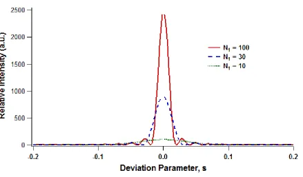
and the total scattering intensity from a thin crystal is then expressed as 𝐼 = 𝐹2𝐽2 = 𝐹2sin
2(𝜋𝑁 1𝑎𝑠1) sin2(𝜋𝑎𝑠
1)
sin2(𝜋𝑁2𝑏𝑠2) sin2(𝜋𝑏𝑠
2)
sin2( 𝜋𝑁3𝑐𝑠3) sin2(𝜋𝑐𝑠
3)
, (2.16)
is reinforced by successive planes of atoms scattering in-phase [64]. Additionally, the width of the diffraction peaks varies inversely with 𝑁1. Therefore, for a thin crystal, diffraction peaks are expected to be broader and less intense than those exhibited by thicker crystals.
Figure 2.6. Scattered intensity as a function of the deviation parameter for different values of 𝑁1. The peak exhibits maximum intensity as 𝑠 = 0. As 𝑁1increases, the peak width is reduced and the maximum intensity is increased.
Such models were later introduced by several scientists, who collectively developed the dynamical theory of diffraction.
2.2.2. Dynamical Theory of Diffraction
Peter Paul Ewald often distinguished between geometrical and kinematical theories. He concluded that the geometrical theories (i.e. Laue’s conditions and Bragg’s law) were useful for determining the directions in which scattered waves reinforce each other without cancellation, while the kinematical theory served to predict total scattered intensities [85]. As demonstrated, experimentally observed intensities are in fact the result of pure geometrical situations, since a diffraction spot is nothing but the Fourier transform of the electron density distribution within the sample. Yet, when investigating real samples, such as thick crystalline substrates and epitaxial layers, neither the geometrical nor kinematical theories prove sufficient to predict diffracted intensities. Consequently, the knowledge provided by these theories must be further extended.
diffracted beam. This diffracted beam also satisfies angular relationships with the set of reflecting planes, allowing for rediffraction to occur. Assuming all waves inside the crystal are plane waves, the energy spread throughout is imagined to concentrate in a triangular region known as the Borrmann fan [64].