HDLC Protocol Implementation Using VHDL
Sarika G. Joshi
1, Vaishali S. Dhongde
2, Prof. Mrs.Mansi Wargantwar
3Assistant Professor, Dept. of Electronics & Teleco mmunicat ion, VA COE, University of Pune,A‟nagar, MH, India 1,2
Assistant Professor, Dept. of Electronics & Teleco mmunicat ion, MITCOE/ Dr. BAMU, Aurangabad, MH, India3
Abstrac t: To successfully transmit data over any network, a protocol is required to manage the flow or space at wh ich the data is transmitted. High-level Data Link Control HDLC is a group of protocols for transmitting synchronous data packets between point-to- point nodes. In HDLC, data is organized into a fra me. It resides on Layer 2 of the Open System Interconnect model, i.e. data lin k layer. HDLC uses zero insertion/deletion process called b it stuffing to ensure that the bit pattern of the delimite r flag does not occur in the fie lds between flags. The HDLC fra me is synchronous and therefore rea lizes on the physical layer to provide method of clocking and synchronizing the transmission and reception of fra mes. It is the most commonly used Layer 2 protocol and is suitable for b it oriented packet transmission mode.[1,2 ]The project analyses the methods of HDLC procedure imple mentation co mmonly used nowadays, & point out their defects. These HDLC procedures are based on Fie ld Progra mmable Gates Array (FPGA) & specially illustrate how to generate Frame Check Sequence i.e . Cyc lic redundancy Check of HDLC in FPGA.These methods are verified by downloading the HDLC modules designed in VHDL into Xilin x9.1 ISE,on FPGA Spartan3 IM Protoboard model - MXS3FK-IM as a target technology, which shows the feasibility of the methods. The p rogra mming modules are simp le, easy to modify, & superior in practica l application. To ma ke the pro ject user friendly a graphica l user interface (GUI) is designed in Visual C ++. Which a llo ws the character byte to enter through keyboard and also shows an o utput data received through GUI
Ke ywor ds: VHDL, FPGA, FSM; FCS generation, CRC, LFSR
I. IN TRO DUC TION
HDLC protocol is the high-level data link control procedures established by International Organizat ion for Standardization (ISO) [1], which are widely used in dig ital co mmun ication and are the bases of many other data link control protocols. There are different set of protocols run on the second layer i.e. Data Lin k Layer.eg. Synchronous Data Link Control (SDLC) Point to Point (PPP) Link Access protocol for Data (LAPD).The fra me format of all these protocol is co mparative ly same . The basic protocol a mongst all t hese protocol is High data link Control (HDLC) protocol.
Currently the HDLC protocol is available in built in the TCP/IP protocol suit, to imp le ment the successful communicat ion over the network environ ment..But, IP Co res are not for free , in order to use wh ich we need to buy the licenses. Software progra mming of HDLC procedures is fle xible, which can be used in many diffe rent HDLC applications by modification of it. However, the progra ms take many resources out of the processor and a lot of time when running, additional to wh ich is the difficu lty of predict ing the signal delays and synchronization. In so me applications of HDLC for mult i-channel signals, the percentage of the resources occupied is proportional to the number of the channels. So software programming is often used in single channels and low-speed signal processing system.
designed separately by the hardware as per the application needed. As the development and wide ly usage of FPGA, HDLC procedures can be imp le mented in FPGA by hardware progra mming. By adopting hardware p rocessing technology, FPGA devices can be programmed repeatedly. Considering speed and fle xibility, FPGA can process mu lti-channel signals in paralle l, and the real-time capacity is predictable and able to be simu lated. In sma ll or med iu m-sized bulk of co mmunication products using FPGAs to replace ASIC devic es for HDLC procedures imple mentation is a proper choice. In this paper, we p ropose a method of HDLC procedures.
II. HDLCPROTOCOLSTRUCTURE
HDLC protocol is bit-oriented protocol which is much mo re fle xib le and more e fficient than character-oriented protocol (such as PPP used in internet) [4]. The basic transfer unit of HDLC protocol is fra me, and its structure is shown as fig. 1.
1 byte 1-2 bytes 1 byte variable 2 byte 1 byte
Flag Address field Control field Information FCS Flag
Fig 1: HDLC frame structure
In the structure, “Flag field” is for the frame synchronization flag, and is the same binary codes “01111110” for both frame header and frame end; as “Address field” is either 1 or 2 byte to hold for the address of receiv ing station. “Control Field” is 1 byte long, used to send the additional control information about the type of data field. “Data field” is on behalf of user data which should be a multip le of 8 b its; [3]
HDLC is the transparent protocol. i.e. In order to avoid the conflict between the duplication of flag sequence in the information frame as user data, it uses the “bit stuffing.”When sending data, if five “1”s emerge continuously in bit stream e xclud ing fra me synchronization flags, we should insert a “0” after the fifth “ 1” manually; when rece iving data, if five continuous “1”s emerge and the next is “0”, we should remove the following “0” to revert the data. HDLC protocol supports three types of fra me structure Information fra me; supervisory fra me; and unnumbered fra me.[1]. The papers discuss the imple mentation of data sending and receiving along with the supervisory control command in a fra me.
A. HDLC Fra me structure
The details of all the fiel ds of HDLC fra me structure is as follo ws.[4,5,6]
Flag field: HDLC uses the 1 byte start and end flag sequence in order to differentiate between start and end of fra me. This flag sequence is constant as “01111110”. HDLC is the transparent protocol. i.e. In order to avoid the conflict between the duplication of flag sequence in the info rmation frame as user data, it uses the “bit stuffing.”When sending data, if five “1”s emerge continuously in b it stream excluding frame synchronization flags, we should insert a “0” after the fifth “1” manually; when receiv ing data, if five continuous “1”s emerge and the next is “0”, we should remove the following “0” to revert the data.
Address field: The address field (A) identifies the primary or secondary stations involvement in the fra me transmission or reception. Each station on the link has a unique address. In an unbalanced configuration, the A field in both commands and responses refer to the secondary station. In a balanced co nfiguration, the command fra me contains the destination station address and the response frame has the sending station's address. The address of the destination can be either 8 bit or 16 b it. Structure of 8 bit address field is as shown in table I.
TABLE I
8 Bit Address Field 1 Bit (Unicast /
Multicast Address)
6 bits(Node Address)
1 Bit End of Address Fie ld( EOAF)
Node address: - the Address copied fro m the last 6 b its of IP address from Network Layer. [17]
End of address field (EOAF): If the value of this one bit fie ld is 1,it indicates the end of address field. and, if 0 indicates the address is 16 bit wide.
Control field: HDLC uses the control field (C) to determine how to control the communicat ions process. This fie ld contains the commands, responses and sequences numbers used to ma intain the data flow accountability o f the link, defines the functions of the frame and init iates the logic to control the movement of data traffic between sending and receiving stations.
The project used the fixed sequence number for the information fra me.
Frame check sequence:FCS” is Frame Check Sequence field of 2 bytes, the calculation of the entire frame, excluding the fra me synchronization flags used to check the correctness of the received data frame sequence. FCS in HDLC procedures adopts Cyclical Redundancy Check (CRC) which is widely used in digita l co mmunicat ion applications.
III. HDLCMODULESDES IGN
To imp le ment the HDLC p rotocol the system is basically d ivided in to t wo sections, i.e. encoding -and-sending module (transmitter section) and receiving-and-decoding module (receiv ing section). The detail bloc k diagra m of the transceiver system is shown in Fig.2.
Fig.2: Transceiver block diagram
A. Transmitter
Fig.3: Sh ift Sequence Using Linear Feedback Shift Register
The final output of transmitter is co mes fro m PISO.The receiver perfo rms a simila r ca lculat ion for a ll address, control, and information bits, as well as for all the FCS fields received. It then compares the result. When a match occurs, the fra me valid status bit is set to '1'. When the result does not match, the rece iver sets the CRC erro r bit to '1'. The transmitter and the receiver automatica lly perform this FCS generation, transmission and checking functions.
B. Receiver.
The 56 bit fra me generated for the 8 bit data fro m the transmitter section is applied to the serial in para llel out of the receiver.The output of SIPO is a co mplete fra me in paralle l fo rm which consists of start flag, address, control, data, and CRC and end flag. The data that is given to the input of transmitter is of 8-b its.At receiver output also we obtain 8-bit data. This data is hold in the data hold circuit If continuous 5 or mo re than 5 one‟s are there in the data field same as that of FLA G fie ld then the additional ZERO is inserted at D5 position to separate data from flag, and set the STUF signal as 1.Project is designed for testing the data as letters A-Z, a-z & a lphabets 0-9, and the special character such as‟,”,:.;~ etc. The character”~” contains the ASCII value same as the flag bits as „01111110‟.Fot this character the data get stuffed out and shows the „stuff data‟ output signal at logic one, that show the Bit Stuffing ,which is the unique feature of HDLC Protocol. This block is used to hold the address of the receiving station which is fixed for the given configuration The new CRC is calculated on the received 8 b it data .The calculat ion and working of receiver CRC is same as the CRC at transmitter side. The calcu lated CRC at the rece iver side is co mpared with the CRC received by transmitter side. If both are found to be equal the CRC error is „zero‟. If no match is found t hen the CRC error is set to „one‟.The Synchronous FIFO is a First-In-First-Out memory queue. Its control logic performs all the necessary read and write pointer management, generates status flags, and generates optional handshake signals for interfac ing with the user logic. It acts as me mory which stores the received 8 character byte. The output of the FIFO is the final output of the receiver.
Fig.4: System Develop ment Flow
GRAPHICALUS ERINTERFACE
To ma ke the system user friendly, mo re effic ient and easy to operate a graphical user interface(GUI) is created in microsoft visual studio2008. The 8 byte character input is given through keyboard to the GUI. This Data input is applied to the Scan code module to scan the data one by one, using RS 232 seria l interface.Then output of scan code is given to the HDLC Transmitter‟s FIFO modu le, for the formation of 56 bit frame structure.
The successfully received data, displayed on the output screen of the GUI, using RS-232 seria linterface.GUI is designed to displaed fra me aborted signal and error signal generated if any.The system is tested for the te xt data, numeric data and a lso for the flag b it as a data input to check the bit stuffing, which is the unique feature o f HDLC protocol.The screen shot input and output display of the GUI for the above said data inputs are shown in Fig. 5 and Fig. 6
Fig.5: Connection Establishment through GUI
IV. RESULT
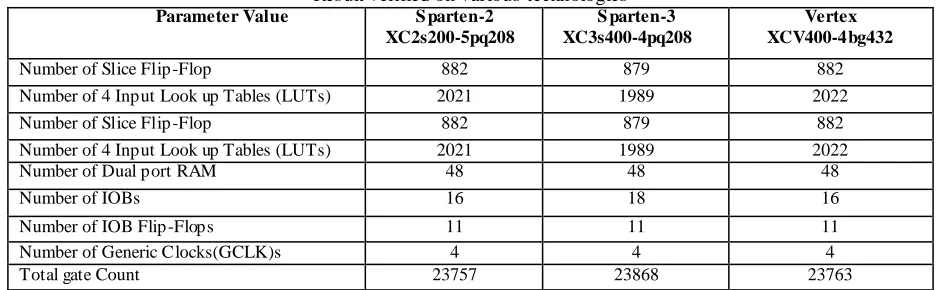
Single channel HDLC protocol Transceiver has been successfully imple mented in the Xilin x Spartan -III series of FPGA.Result of the system developed is observed on Spartan -II and Spartan-III shown in table II.
TABLE II
Result verified on various technologies
Parameter Value S parten-2 XC2s200-5pq208
S parten-3 XC3s400-4pq208
Vertex XCV400-4bg432
Number of Slice Flip -Flop 882 879 882
Number of 4 Input Look up Tables (LUTs) 2021 1989 2022
Number of Slice Flip -Flop 882 879 882
Number of 4 Input Look up Tables (LUTs) 2021 1989 2022
Number of Dual port RAM 48 48 48
Number of IOBs 16 18 16
Number of IOB Flip -Flops 11 11 11
Number of Generic Clocks(GCLK)s 4 4 4
Total gate Count 23757 23868 23763
Performance para meter are also compared with the previous work done are summarized in the table III [11,12,13]
TABLE III
Co mparison with Prev ious work done
Parameter Value Single Channel HDLC Transmitter
MT8952B Based HDLC Transceiver
S parten-3 XC3s400-4pq208
Number of Slice Flip -Flop 316 ---- 879
Number of 4 Input LUTs ---- 4289 1989
Number of Dual port RAM ---- ---- 48
Number of IOBs 68 21 18
Number of IOB Flip -Flops ---- 9 11
Number of GCLKs ---- 4 4
Total Gate Count ---- 35037 23868
V.CO NC LUSION
During the develop ment of the VHDL code, it has been a goal to ma ke it synthesizable. By synthesizing the design, some constrains on areas and timing has been found. This increase linearly with increase in para meters and that a re taken as a proof that the VHDL mode l could be synthesized well. Each module of the transceiver is thoroughly simu lated both before and after synthesis and is well optimized. The advantage of imp le menting this HDLC protocol transceiver in FPGA is that it gives fle xibility, upgradability and customizat ion benefits of p rogra mmable logic device. Fro m a ll the above results it is concluded that better system utilizat ion is done on Spartan -III as compared to the Spartan-II, single channel HDLC t ransmitter and also MT8952B Based HDLC Transceiver.
Using internal storage in FPGA, It solves the problem that Application Specific Integrated Circuits (ASICs) require e xternal storage devices.HDLC is a basic p rotocol fro m the data lin k layer control. As it is designed successfully, n ow, it can be further upgraded to any other protocol by ma king the changes in the structure of control field of that particular protocol.
AC KNOWLEDGMEN T
throughout the period this work was carried out. Her readiness for consultation at all times, her concern and assistance even with practical things have been extre me ly helpful. It was a great pleasure to work under her guidance.My sincere thanks to all the teaching and non-teaching staff me mbe rs of my co llege and those who knowingly and unknowingly have contributed in their own way in co mpletion of th is work.
REFER ENC ES
[1] Andrew S. T enenbaum ,”Computer Networks”, ,PHI,ISBN 81-203 2175-8, 4th Edition, pp. 16-23, 175-183, 187-190, 225- 228. [2] Fourauzan B, “ Data communication and Computer Networks”, Tata McGraw Hill, 4th Edition, pp. 284-294,340-344.
[3] James F. Kurose, Ross, “ Computer Networking-a top down approach featuring the internet “, Pearson Education, 3rd Edition, pp. 28 -36, 72-78, 445-456.
[4] Comer D. “ Computer networks and internet”, Pearson Education, 4th Edition, pp.78-80.
[5] Olifer&Olifer,”Computer Networks-principles, technologies & protocols for network design”, Wiley, pp. 108-126.
[6] S. HamedJavadi and Ali Peiravi , “ Design & implementation of High bit Rate HDLC transceiver Based on a modified MT8952B Controller”, INSInet Publication, 2009, pp. 4125-4131.
[7] Jun Wang, Wenhao Zhang, Yuxi Zhang, Wei Wu“ Design and Implementation of HDLC Procedures Based on FPGA” School of Electronic and Information Engineering Beihang University (BUAA) Beijing, China, pp. 20-22.
[8] ISO/IEC 13239, “ Information technology --T elecommunications and Information exchange between systems – High-level data link control (HDLC) procedures,” International Organization for Standardization, July 2002, pp. 10-17.
[9] William Stallings, “ Data & Computer Communication”, Prentice Hall of India 2000, 7th Edition, pp. 171-180,207-213. [10] William Stallings, “Wireless Communication and Networks” Prentice hall of India 2000, 2nd Edition, pp.192 -201.
[11] Syed ManzoorQasim and Shuja A. Abbasi,” FPGA Implementation of a Single-Channel HDLC Layer-2 Protocol Transmitter using VHDL”, ICM 2003, Dec. 9-11, Cairo, Egypt, pp. 265-268.
[12] GAO Zhen-Bin LIU Jian-Fei, “ FPGA implementation of a multi- channel HDLC protocol transceiver” School of Information Engineering Hebei University of T echnology T ianjin, China, pp. 1300 -1302.
[13] K. Sakthidasan, mohammedMohammed,”DESIGN& Implementation of HDLC Controller using VHDL”, International Journal of Science & Engineering Research, Volume 2, Issue 3,March-2011, ISSN 2229-5518.
[14] Request For Comments: 3572 & RFC 2176.
[15] Michael Gschwind&Valentinaalapura, “ VHDL Design Methodology for FPGAs ”, Technische University WiCn.
[16] K.C. chang, “Digital Design &Modelling with VHDL and Synthesis”, IEEE Computer Society Press 1997, pp. 177-185,242-246 [17] J.F. wakerly, “Digital Design principle & Practice”, Prentice Hall New Jersey, 2000, pp. 542-553,850-858

![2,2′ {[2 (Pyridin 2 yl) 1,3 diazinane 1,3 diyl]bis(methylene)}diphenol](data:image/gif;base64,R0lGODlhAQABAIAAAP///wAAACH5BAEAAAAALAAAAAABAAEAAAICRAEAOw==)