ISSN(Online): 2319-8753 ISSN (Print): 2347-6710
International Journal of Innovative Research in Science,
Engineering and Technology
(A High Impact Factor, Monthly, Peer Reviewed Journal)
Visit: www.ijirset.com
Vol. 8, Issue 2, February 2019
Testing of an IC Using Debugging Method
A.N. Sivadharshani M.E., C.I.Vimalarani M.E.,
Assistant Professor, Dept. of ECE, Mangayarkarasi College of Engineering, Paravai, Madurai, Tamilnadu, India
Assistant Professor, Dept. of ECE, Mangayarkarasi College of Engineering, Paravai, Madurai, Tamilnadu, India
ABSTRACT: With the growing size of modern designs and more strict time-to-market constraints, design errors unavoidably escape pre-silicon verification and reside in silicon prototypes. As a result, silicon debug has become a necessary step in the digital integrated circuit design flow. Although embedded hardware blocks, such as scan chains and trace buffers, provide a means to acquire data of internal signals in real time for debugging, there is a relative shortage in methodologies to efficiently analyze this vast data to identify root-causes. This paper presents a BIST technique that attempts to fill-in the gap. The presented techniques automate the configuration process for trace-buffer based hardware in order to acquire helpful information for debugging the failure, and detect suspects of the failure in both the spatial and temporal domain.
KEYWORDS: BIST, LFSR, FPGA, Fault Detected, Reduction of power and error.
I. INTRODUCTION
This project presents the details about the on-line Built-In Self-Test (BIST) and BIST-based diagnosis of programmable logic resources in Field Programmable Gate Arrays (FPGAs). The BIST approach provides complete testing of the programmable logic blocks (PLBs) in the integratedcircuitsduring normal system operation. The BIST-based diagnosis can identify any group of faulty PLBs, and then applies additional diagnostic configurations to identify the faulty flip flop within a faulty PLB. The ability to locate defective modules inside a PLB enables a new form of fault-tolerance that reuses partially defective PLBs in their fault-free modes of operation. A new reseeding architecture for scan-based built-in self-test (BIST), which uses a linear feedback shift register (LFSR) as test pattern generator. The LFSR generates the same state sequence, keeping that way the implementation cost low. A seed-selection algorithm is furthermore presented that, it manages to significantly reduce the number of the required seeds for achieving complete (100%) fault coverage. Experimental results demonstrate the advantages of the proposed linear feedback register reseeding approach over the already known reseeding techniques. At the most basic level, FPGAs consist of programmable logic blocks, routing (interconnects), and programmable I/O blocks Almost 80% of the transistors inside an FPGA device are part of the interconnect network. FPGAs present unique challenges for testing due to their complexity. Errors can potentially occur nearly anywhere on the FPGA. Faults may occur due to logical or electrical design error, manufacturing defects, aging of components, or destruction of components (due to exposure to radiation). FPGA tests should detect faults affecting every possible mode of operation of its programmable logic blocks and also detect faults associated with the interconnects. PLB testing tries to detect internal faults in one or more than one PLB
Faults in SRAM-based FPGA’s can be classified as one of the following: Stuck at faults, also known as transition
faults, occur when normal state transition is unable to occur. The two main types are stuck at 1 and stuck at 0. Stuck at 1 faults result in the logic always being a 1. Stuck 0 results in the logic always being a 0. The stuck at model seems
simple enough, however, the stuck at fault can occur nearly anywhere within the FPGA. Bridging faults occur when
two or more of the interconnect lines are shorted together. The operation effect is that of a wired and/or depending on
ISSN(Online): 2319-8753 ISSN (Print): 2347-6710
International Journal of Innovative Research in Science,
Engineering and Technology
(A High Impact Factor, Monthly, Peer Reviewed Journal)
Visit: www.ijirset.com
Vol. 8, Issue 2, February 2019
extraction [3].This method overcomes the major drawback associated withscan-based techniques by allowing signals to be observed overmultiple clock cycles, at full circuit speed, so that the behaviorof the device can be analyzed over time. Once an error has been detected, however, the designer needs to find the root cause of that incorrect behavior; this is the task we refer to as “silicon debugging.” For this, coverage-based metrics are notappropriate since it is no longer necessary to show that a bugexists, but instead, to deduce the design error that led to theobserved incorrect behavior. II.Frame Works
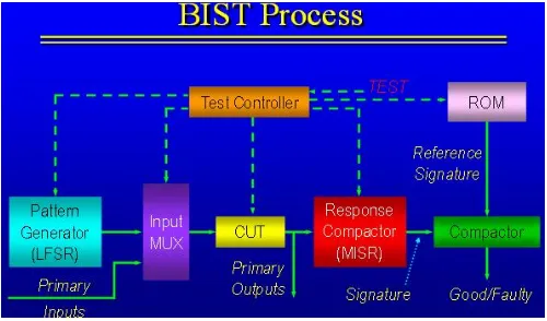
In this paper, we are concerned only with debugging functional errors using BIST and trace-based techniques. The BIST architecture can be simple or complicated based on the purpose of the test being performed on the circuit. A basic
BIST architecture for testing an FPGA includes a controller, pattern generator, the circuit under test, and a response analyzer.
Figure.1
A. Bist Block Diagram
We assume an integrated circuit that has been instrumented with one or more trace buffers, as illustrated in Fig. 1. The trace buffers are used to continuously record a history of selected signals over time, possibly using on-chip compression schemes We assume that the chip is also instrumented with programmable trigger circuitry (possibly driven by an external source)to halt the chip when a specific condition occurs, so that a trace of states surrounding the error can be extracted for analysis. In this paper, we focus on circuits with a single clock, but the methods described can be extended to multiple clock systems due to the fact that trace buffers can only be used to instrument signals within
their own clock domain. A BIST have apseudo-random binary sequence (PRBS) generator and a signature
register. The PRBS generator is most easily implemented using a linear feedback shift register (LFSR). A PRBS generator allows us to generate all of the required binary patterns for the circuit under test. The LFSR can be used to both generate the test sequence for the design that is to incorporate BIST and with slight modification can be used to capture the response of the design and generate a signature.
It is a unit which is used for generating the test signals; this is done by methods called Exhaustive / Pseudo Exhaustive
Testing. In exhaustive testing all possible input patterns are applied to the circuit under test. Thus to an n input combinational circuit all possible 2^n patterns are applied to the circuit. The advantage of this approach is that all redundant faults can be detected. A modified form of exhaustive testing is Pseudo Exhaustive Testing. It retains the advantages of exhaustive testing while significantly reducing the number of test patters to be applied. The basic idea is to partition the circuit under test into several sub circuits such that each sub circuit has a few enough inputs for exhaustive testing to be feasible for it. If the output response of the circuit under test do not match the expected response when the stored test patterns are applied in the presence of a fault.
ISSN(Online): 2319-8753 ISSN (Print): 2347-6710
International Journal of Innovative Research in Science,
Engineering and Technology
(A High Impact Factor, Monthly, Peer Reviewed Journal)
Visit: www.ijirset.com
Vol. 8, Issue 2, February 2019
B. Linear Feedback Shift Register The general representation on of LFSR based the primitive polynomial is given by
P(x)= xn + pn-1xn-1 + ………p2x2 + p1x + p0
CIRCUIT UNDER TEST:
CUT is simulated with a random pattern sequence of a random length. The pattern is then generated by an algorithm and implemented in the hardware. If the response is correct, the circuit contains no faults. The problem with pseudo-random testing is that is has a low fault coverage unlike the exhaustive pattern generation method. It also takes a longer time to test. A relationship between a pseudo random test sequence of length L and the fault coverage E (c) is given by
Test Response Analyzer
The most important part of the BIST architecture is the test response analyzer (TRA). Like the pattern generator, its
uses one output generator It is designed based on the diagnostic requirements Theresponse analyzer usually contains
comparator logic. Two comparators are used to compare the output of two CUTs. The two CUTs must be exact. The registered and unregistered outputs are then put together in the form of a shift register. The function generator within the response analyzer compares the outputs. The outputs are then OR ed together .Once compared, the function generator gives a response back of a high or low depending on if faults are found or not.
THE BIST PROCESS
The test controller is used to start the test process. The pattern generator produces the test patterns that are inputted into the circuit under test. The CUT is only a piece of the whole FPGA chip that is being tested on and found within a configurable logic block or CLB The FPGA is not tested all at once but in small sections or logic blocks. After a test vector scans the CUT the output of the test is analyzed in the response analyzer. It is compared against the expected output. If the expected output matches the actual output provided by the testing, the circuit under test has passed. Within a BIST block, each CUT is tested by two pattern generators. The output of a response analyzer is inputted to the pattern generator/response analyzer cell this process is repeated throughout the whole FPGA, a small section at a time. The output from the response analyzer is stored in memory for diagnosis.
III. EXPERIMENT AND RESULT
The table represents the true and fault output and also it determines the type of fault occurred in the integrated circuits.
Table.1 S.N o Input data Text pattern generat or Flag regist er Fault output Correct output
1. 11111 10111 11110 SC fault 11111 2. 11111 11101 11101 OCfault 11111 3. 11111 11011 11011 Delay 11111
2n-1
E(c) = 1-∑(1-L/2n)k hk/M
ISSN(Online): 2319-8753 ISSN (Print): 2347-6710
International Journal of Innovative Research in Science,
Engineering and Technology
(A High Impact Factor, Monthly, Peer Reviewed Journal)
Visit: www.ijirset.com
Vol. 8, Issue 2, February 2019
a.Implementation table
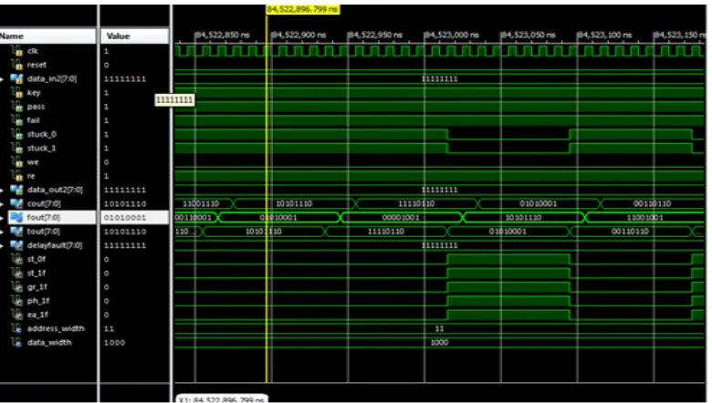
Simulated output:
FIGURE -3(STIMULATED OUTPUT)
ISSN(Online): 2319-8753 ISSN (Print): 2347-6710
International Journal of Innovative Research in Science,
Engineering and Technology
(A High Impact Factor, Monthly, Peer Reviewed Journal)
Visit: www.ijirset.com
Vol. 8, Issue 2, February 2019
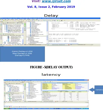
FIGURE -5(DELAY OUTPUT)
FIGURE-6(LATENCY OUTPUT)
IV. CONCLUSION
IC testing is becoming more and more important as FPGAs themselves grow to be faster and larger. Fault errors that occur within a chip need to be located and dealt with so that the FPGA can work properly. A built-in-self-test is one way of testing an IC internally without the use of external components. The BIST test uses architecture found within the FPGA to perform the testing. The FPGA is broken down into smaller section or logic blocks where the testing takes place. In each section, a pattern generator sends a test vector into the circuit being tested on. The output is then analyzed in the response analyzer and stored in memory where it is later evaluated. This process is continued until the whole IC is tested. The advantage of the BIST test is that it can be done while the IC is online. Another advantage is that the test is done internally and no expense is used on external components.
REFERENCES
ISSN(Online): 2319-8753 ISSN (Print): 2347-6710
International Journal of Innovative Research in Science,
Engineering and Technology
(A High Impact Factor, Monthly, Peer Reviewed Journal)
Visit: www.ijirset.com
Vol. 8, Issue 2, February 2019
4. H. F. Ko and N. Nicolici, “Algorithms for state restoration and trace-signal selection for data acquisition in silicon debug,” IEEE Trans. Comput.-Aided Design Integr. Circuits Syst., vol. 28, no. 2, pp. 285– 297, Feb. 2009.
5. J.-S. Yang and N. Touba, “Automated selection of signals to observe for efficient silicon debug,” in Proc. 27th IEEE VLSI Test Symp. ,May 2009, pp. 79–84.
6. J. Gao, Y. Han, and X. Li, “A new post-silicon debug approach based on suspect window,” in Proc. 27th IEEE VLSI Test Symp., May 2009, pp. 85–90.
7. Kaivola, R. Ghughal, N. Narasimhan, A. Telfer, J. Whittemore, S. Pandav, Slobodová, C. Taylor, V. Frolov, E. Reeber, and A. Naik, “Replacing testing with formal verification in Intel(R) Core(TM) i7 processor execution engine validation,” in Proc. 21st Int. Conf. Comput. Aid. Verificat., 2009, pp. 414–429.
8. Liu and Q. Xu, “Trace signal selection for visibility enhancement in post-silicon validation,” in Proc. Design, Autom. Test Eur., Nice, France, Apr. 2009, pp. 1338–1343.
9. B. R. Quinton, A. M. Hughes, and S. J. E. Wilton, “Post-silicon debug of complex multi clock and power domain SoCs,” in Proc. Design, Autom. Test Eur. Conf., Mar. 2009, pp. 1–6.
10. M. Abramovici, P. Bradley, K. Dwarakanath, P. Levin, G. Memmi, and D. Miller“Areconfigurable design-for-debug infrastructure for SoCs,” in Proc. 43rd Annu. Design Autom. Conf., 2006, pp. 7–12.
11. B. Quinton and S. Wilton, “Post-silicon debug using programmable logic cores,” in Proc. IEEE Int. Conf. Field-Program. Technol. , Dec. 2005, pp. 241–247.
BIOGRAPHY
A.N.Sivadharshani born in Madurai, Tamil Nadu (TN), India, in 1991. she received her B.E. degree in Electronics and Communication Engineering from Sethu Institute Of Technology, Madurai, Anna University, Chennai, India, in 2007 and M.E. (VLSI Design) from Sethu Institute of Technology,Virudhunagar, Anna University, Chennai, India. She is presently working as an Assistant Professor in the department of ECE at Mangayarkarasi college of Engineering,Madurai,Tamilnadu, India. Herresearch interest includes Digital Signal Processing, Neural Networks and Genetic algorithms,Layout Design In VLSI.