Performance Analysis of Multi-Rate Approach
based Adaptive Filter
Shalu Khan1, Amjad Khan2
M. Tech. Scholar, Department of Electronics and Communication, SISTec, Bhopal, India1
Assistant Professor, Department of Electronics and Communication, SISTec, Bhopal, India2
ABSTRACT: - More and more people around the world suffer from digital signal processing research field. The increase hardware complexity and increase area are the main reasons for this field. The multi-rate approach used for narrow band filter is designed and implemented in Xilinx Vertex-E XCV50E device family. The multi-rate approach is design using the decimator and interpolator structure in VHDL. Each structure is simulated using Xilinx Vertex-E XCV50E device family and compared the existing structure. The resulting structure is hardware efficient and consumes less slices compared to existing structure.
KEYWORDS: Filter Coefficient, Finite Impulse Response, Pass-band Frequency, Narrow Band Filter.
I. INTRODUCTION
Multi rate simply means "multiple sampling rates". A multi rate DSP framework utilizes different testing rates inside the framework. At whatever point a flag at one rate must be utilized by a framework that anticipates an alternate rate, the rate must be expanded or diminished, and some preparing is required to do as such. Along these lines "Multi rate DSP" truly alludes to the workmanship or study of changing testing rates. Multi-rate preparing discovers use in flag handling frameworks where different sub-frameworks with varying example or clock rates should be interfaced together. At different occasions multi-rate preparing is utilized to decrease computational overhead of a framework. For instance, a calculation requires k tasks to be finished per cycle. By diminishing the example rate of a flag or framework by a factor of M, the number-crunching transfer speed prerequisites are decreased from kfs activities to kfs/M tasks every second. Customary converters are regularly hard to actualize in scarcely discernible difference huge scale coordination (VLSI) innovation. By remembering these things the general population is going for over examining converters, these converters make broad utilization of computerized flag handling.
Higher reliability.
Increased functionality.
Reduced chip cost.
Those attributes are regularly required in the advanced flag handling condition of today. An essential use of computerized flag handling techniques is in deciding in the discrete-time do-fundamental the recurrence substance of a ceaseless time flag, all the more generally known as unearthly examination. All the more specifically, it includes the assurance of either the vitality range or the power range of the flag.
Practically all melodic projects are delivered in essentially two phases. To start with, sound from every individual instrument is recorded in an acoustically dormant studio on a solitary track of a multitrack recording device.
At that point, the signs from each track are controlled by the sound architect to include unique sound impacts and are joined in a blend down framework to finally produce the stereo chronicle on a two-track recording device.
The remainder of the paper is organized as follows: multi-rate approach algorithm is presented in Section II. The proposed structures of narrow band filter are presented in Section III. Hardware and time complexity of the proposed structures are discussed and compared with the existing structures in Section IV. Conclusion is presented in Section V.
II. MULTIRATEAPPROACH
The procedure of changing over a flag from an offered rate to an alternate rate is called testing rate transformation. The frameworks which utilize various examining rates in the handling of advanced flag are called multi-rate flag preparing [5].
Annihilation is the procedures of bringing down the word rate of a carefully encoded flag, which is inspected at high frequencies much over the nyquist rate. It is typically done to build the goals of an oversampled flag and to expel the out-of-band clamor. In a sigma-delta ADC, oversampling the simple information motion by the modulator alone does not bring down the quantization commotion; the ADC should utilize an averaging channel, which fills in as a decimator to expel the clamor and to accomplish higher goals. An essential square diagrammatic portrayal of the decimator is appeared in Figure 1.The decimator is a blend of a low pass channel and a down sampler. In Figure 1 the exchange work, H(z) is illustrative of performing both the activities. The yield word rate of the decimator is down inspected by the factor M, where M is the oversampling proportion [6]. The capacity of low pass separating and down testing can be done utilizing an averaging circuit. The exchange capacity of the averaging circuit is given by condition (1.1). It sets up a connection between the information and yield capacities (1.1)
1 01
)
(
)
(
)
(
M x xz
M
Z
Y
Z
X
Z
H
(1)"Up sampling" is the way toward embeddings zero-esteemed examples between unique examples to expand the examining rate. (This is classified "zero-stuffing".) Up testing adds to the first flag undesired ghastly pictures which are fixated on products [7] of the first inspecting rate.
"Introduction", in the DSP sense, is the procedure of up-examining pursued by sifting. (The separating evacuates the undesired phantom pictures.) As a straight procedure, the DSP feeling of insertion is to some degree not the same as the "math" feeling of addition, yet the outcome is reasonably comparable: to make "in the middle of" tests from the first examples.
Y(Z) X(Z)
H(Z)
Sampling Frequency fs
After Decimator Sampling Frequency
fs/M
Since addition depends on zero-stuffing you can just interject by number components; you can't insert by fragmentary variables. (Be that as it may, you can join insertion and annihilation to accomplish a general sane factor, for instance, 4/5 Up-examining adds undesired phantom pictures to the flag at products of the first inspecting rate, so except if you expel those by separating, the up-tested flag [7] isn't equivalent to the first: it's contorted.
A few applications might have the capacity to endure that; for instance, if the pictures get expelled later by a simple channel, yet in many applications you should evacuate the undesired pictures through advanced sifting. Along these lines, introduction is undeniably increasingly normal [8] that up-inspecting alone.
III. PROPOSEDSTRUCTURE
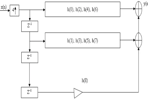
In this work the design of a decimation filter is presented for integrating with an existing designed modulator to form a complete sigma-delta ADC. We use multi-organize destruction channel which implies the single pulverization channel is supplanted by fell channels. In this part, we will discuss the channel engineering utilized in this work, including their structures, qualities and downsides. the initial phase in structuring an obliteration channel is to choose which sorts of channels will be utilized and where demolition will happen. This section investigates the issues associated with picking channel design for a listening device application. The general intensity of a few designs is analyzed, bringing about the three-arrange engineering that is picked to actualize this channel.
A typical need in gadgets and DSP is to confine a restricted band of frequencies from a more extensive data transmission flag. Narrowband channels rather catch just a little piece of the range. They are said to have a thin band-pass. The band-pass is basically the amount of the range the channel permits to band-pass. This is typically estimated in nanometers. Limited band channel comprises of decimator, restricted band and interpolator.
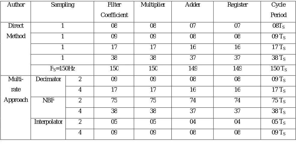
Author Sampling Filter
Coefficient
Multiplier Adder Register Cycle
Period
Direct
Method
1 08 08 07 07 08TS
1 09 09 08 08 09 TS
1 17 17 16 16 17 TS
1 38 38 37 37 38 TS
FS=150Hz 150 150 149 149 150 TS
Multi-rate
Approach
Decimator 2 09 09 08 08 09 TS
4 17 17 16 16 17 TS
NBF 2 75 75 74 74 75 TS
4 38 38 37 37 38 TS
Interpolator 2 05 05 04 04 05 TS
4 09 09 08 08 09 TS
Table 1: Theoretical Analysis of Direct Method and Multi-rate Approach for Different Filter Coefficient and Sampling Frequency
Previous Approach
Proposed Approach
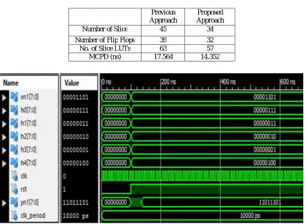
Number of Slice 45 34
Number of Flip Flops 39 32 No. of Slice LUTs 63 57
MCPD (ns) 17.564 14.352
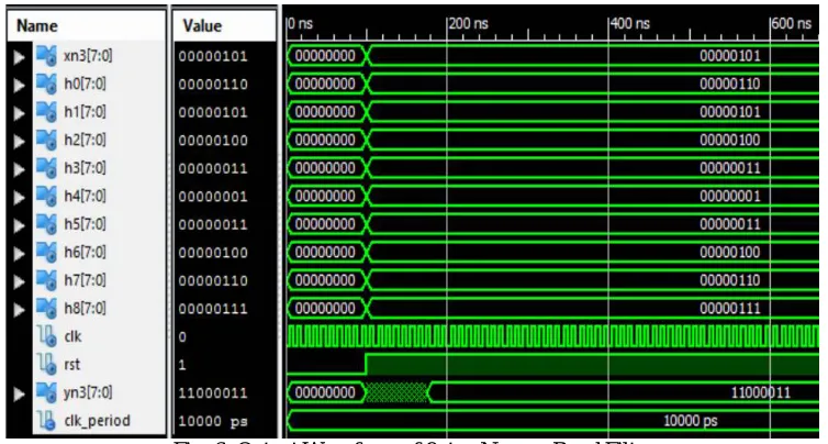
The design as were discussed in figure 3 and figure 4 were implemented using VHDL and then were tested on model sim to determine the number of slice and maximum high frequency. In figure 5, figure 6 and figure 7 have shown the output waveform of narrow band filter and chat between filter order and slices. In figure 7, compare the result between numbers of slice and filter order. Increase the filter order also increase the number of slice shown if figure 7.
Table 3: Comparison Result for Previous and Proposed Approach for N=9
Previous Approach Proposed Approach
Number of Slice 74 66
Number of Flip Flops 71 64
No. of Slice LUTs 141 113
MCPD (ns) 22.432 17.085
Table 2: Comparison Result for Previous and Proposed Approach for N=5
Fig. 6: Output Waveform of 9_tap Narrow Band Filter
V. CONCLUSION
The narrowband filter is realized in FIR filter. Based on the direct approach, the filter requires 150 filter coefficients to meet the desired frequency response. To implement such a large order FIR filter in hardware involves large resources and sometime difficult to implement in resource constrained application. Keeping this in view, we have used Multirate approach to design the narrowband filter. We have used down sampling factor 2 and 4 for this purpose and found that, down sampling factor 4 requires significantly less filter constants than 2. To implement the narrowband filter, we therefore chosen down sampling factor 4 and designed the decimator, interpolator and narrowband filter. The total number of filter coefficients required to realize the decimator, interpolator and the narrowband filter 64 which is almost 58% less than the direct method.
REFERENCES
[1] Azadeh Safari, Yinan Kong, “Four tap Daubechies filter banks based on RNS”, 2012 International Symposium on Communications and Information Technologies (ISCIT) 978-1-4673-1157-1/12/$31.00 © 2012 IEEE.
[2] Dr. Pawan K. Gaikwad, “Field Programmable Gate Array Implementation of Digital Filter ofHighest-Possible Order and its Testing using AdvancedMicrocontroller”,IJREAT International Journal of Research in Engineering & Advanced Technology, Volume 1, Issue 4, Aug-Sept, 2013.
[3] M.RAVI KUMAR, “ELECTROCARDIOGRAM (ECG) SIGNAL PROCESSING ON FPGA FOR EMERGING HEALTHCARE APPLICATIONS ”, International Journal of Electronics Signals and Systems (IJESS) ISSN: 2231- 5969, Vol-1 Iss-3, 2012.
[4] Pramod Kumar Meher, Senior Member, IEEE, Shrutisagar Chandrasekaran, Member, IEEE, and Abbes Amira, Senior Member, IEEE, “FPGA Realization of FIR Filters by Efficient and Flexible Systolization Using Distributed Arithmetic”, IEEE TRANSACTIONS ON SIGNAL PROCESSING, VOL. 56, NO. 7, JULY 2008.