IJEDR1603143
International Journal of Engineering Development and Research (www.ijedr.org)887
Implementation of a Low drop out regulator using a
Sub 1 V Band Gap Voltage Reference circuit in
Standard 180nm CMOS process
1
S.Aparna,
2Dr. G.V. Mahalakshmi
1PG Scholar, 2Professor
1,2Department of Electronics and Communication Engineering 1,2Sreenidhi Institute of Science and Technology, Hyderabad, India
________________________________________________________________________________________________________
Abstract—A low drop out regulator (LDR) is implemented using a Sub 1 V Band Gap Reference (BGR) in standard 180nm CMOS process. In low dropout regulators the unregulated output is very close to that of regulated one. In this sub 1 V Band Gap Reference (BGR), the reference voltage is obtained by super imposing the Complementary to Absolute Temperature (CTAT) and Proportional to Absolute Temperature (PTAT) modules in current mode and little amount of current is superimposed through the circuit to nullify the Current Mirror variations in Reference Voltage. The Temperature Coefficient of the BGR is 10ppm/°C in the range of 0-100°C and the line regulation is 1.46mV/V for the supply variations of 0.8-1.8Vand PSRR is 45.8dB @1Hz.The output Voltage of the LDR is 0.7V for the Input Supply range 0.8-1.8V. The drop out voltage is 0.1 V and the quiescent current is 19.6µA.
Index Terms---Dropout Voltage, low voltage, low drop out regulator and Sub 1 V band gap reference.
________________________________________________________________________________________________________
I. INTRODUCTION
There is a huge demand for portable devices operated by battery in recent years. This led the desire for long battery life. To prolong the battery life there is a need for efficient power management circuits. These circuits must operate at low voltage and currents in order to maximize the battery life time. As the process technology is scaled down, the operating voltage of the devices is getting reduced. The Low dropout regulators find application in portable devices such as cell phones, laptops, tablet PC’s etc. which require low regulated voltage.
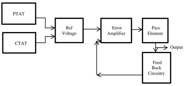
In low dropout regulators the unregulated output is very close to that of regulated one. The Major blocks of the low dropout Regulator are Band gap Voltage reference, Error amplifier, power transistor (pass element) and some feedback circuitry as sho wn in Fig. 1. The Reference Voltage for Low dropout regulator is given from Bandgap Voltage reference, which provides constant voltage independent of supply and temperature variations. The output Voltage of Conventional Band Gap Reference is greater than 1 V. But the portable devices require less than 1 V supply so Voltage reference which works under the supply of 1V is very much required in these days.
Conventional Band Gap References are based on bipolar devices [1-2] and the output is also greater than 1V. Resistive Subdivision technique is proposed which works for the supply less than 1V [3]. Many other techniques have been proposed Such as Dynamic Threshold MOS (DTMOS) Technique [4], in which the material band gap is lowered by using electro static field and requires additional fabrication steps. A Band Gap Reference Circuit using transimpedance amplifier is proposed [5] it requires a supply voltage greater than 1 V. A Band Gap Reference using resistive divider technique is proposed [6] and it solved the limited input common mode range of operational amplifier. Band Gap Reference using body driven technique [8] is proposed it operates at low voltage without requiring low threshold voltage devices but it has MOS Transistor offset effect. A 1 V Band Gap Reference [9] is proposed in which one to one resistor matching is used for improved matching and has poor performance due to process variations. Curvature Compensation technique [10] is proposed the reference voltage obtained with very low sensitivity to temperature but there are some mismatches. In [12] the reference voltage is obtained by super imposing the Complementary to Absolute Temperature (CTAT) and Proportional to Absolute Temperature (PTAT) modules in current mode and has current mirror variations in the reference voltage. A MOSFET based LDR [14] is designed using series n-channel MOSFET and used conventional Band gap reference and consumes more power. In [15] LDR is designed in BCD technology for supply voltage 2 V to reduce the quiescent current. In an NMOS LDR based on the dynamic biasing technique [16] for driving gate of the pass transistor the regulated output is 1 V. In [17] a LDR with buffer added before the pass element in order to have a fast transient response.
IJEDR1603143
International Journal of Engineering Development and Research (www.ijedr.org)888
II. SUB1 V BAND GAP REFERENCE AND LOW DROP OUT REGULATOR CIRCUITIn this paper, a low dropout regulator using a Sub 1 V Band Gap Voltage Reference is designed in 180nm standard CMOS process. In the Sub 1 V BGR little amount of current is superimposed through the circuit to nullify the Current Mirror variations in Reference Voltage with Supply Voltage.
i. Sub 1 V Band gap reference circuit
Fig. 2 Sub 1 V Band Gap Reference
The Sub 1 V Band gap reference is shown in Fig.2. The pnp transistor Voltage is 0.6 V. The static input Voltage of operational amplifier is stabilized at 0.1 V by adjusting the resistors R1, R2. So the circuit operates normally even when the supply voltage is 0.9 V. The operational amplifier is used to make both potentials equal. The transistor PM1 and PM4 forms the current source and the bias voltage is given from the output Voltage of the operational amplifier. The PTAT current at the node near to R0 is mirrored using PM2 transistor which acts as a current source. The transistor NM6 is operated in linear region. For the transistor Q3 the constant current is supplied through PM3 transistor which acts as a current source with bias voltage as the operational amplifier output voltage and the CTAT current is obtained at the node. The PTAT and CTAT currents are translated into Voltages by using resistors R5 and R6 respectively and the reference Voltage is by adding the Voltages in series and the reference voltage obtained at the REF. From NM1 transistor some amount of current is super imposed to the PTAT current in order to reduce the current mirror variations in the reference voltage with the supply voltage.
ii. 0.8 V Operational Amplifier
IJEDR1603143
International Journal of Engineering Development and Research (www.ijedr.org)889
Fig. 3 0.8 V Operational AmplifierNM1 transistors, which makes the same current to flow in the both branches of the differential pair. The capacitance C0 is used to lower the gain of the op amp at high frequencies. The gain of the operational amplifier obtained is 52 dB for the supply voltage 0.9 V and the static input voltage is 0.1 V.
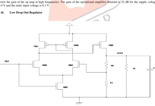
iii. Low Drop Out Regulator
IJEDR1603143
International Journal of Engineering Development and Research (www.ijedr.org)890
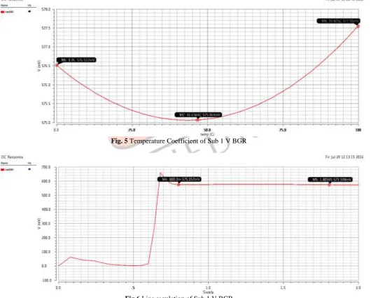
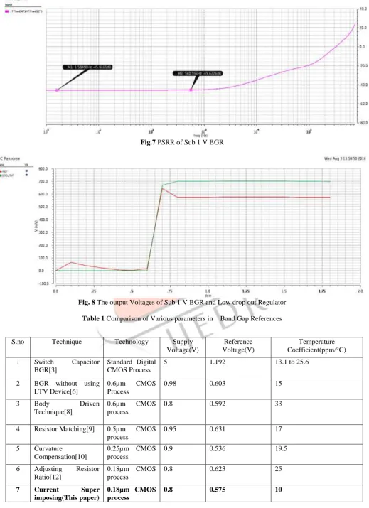
Voltage for LDR is 0.7V in the Input Supply range 0.8-1.8V is shown in Fig. 8. The dropout voltage is 0.1 V and the quiescent current is 19.6µA. The Power dissipation of the Low drop out regulator including BGR is 0.2mW. Table I shows the comparison of parameters like minimum supply voltage, reference voltage, temperature coefficient, technology used etc. of various Band gap references.Fig. 5 Temperature Coefficient of Sub 1 V BGR
IJEDR1603143
International Journal of Engineering Development and Research (www.ijedr.org)891
Fig.7 PSRR of Sub 1 V BGRFig. 8 The output Voltages of Sub 1 V BGR and Low drop out Regulator
Table 1 Comparison of Various parameters in Band Gap References
S.no Technique Technology Supply
Voltage(V)
Reference Voltage(V)
Temperature Coefficient(ppm/°C) 1 Switch Capacitor
BGR[3]
Standard Digital CMOS Process
5 1.192 13.1 to 25.6
2 BGR without using LTV Device[6]
0.6µm CMOS Process
0.98 0.603 15
3 Body Driven
Technique[8]
0.6µm CMOS process
0.8 0.592 33
4 Resistor Matching[9] 0.5µm CMOS process
0.95 0.631 17
5 Curvature
Compensation[10]
0.25µm CMOS process
0.9 0.536 19.5
6 Adjusting Resistor Ratio[12]
0.18µm CMOS process
0.8 0.623 25
7 Current Super
imposing(This paper)
0.18µm CMOS process
IJEDR1603143
International Journal of Engineering Development and Research (www.ijedr.org)892
[2] B. Razavi, Design of Analog CMOS Integrated Circuits: T. McGraw- Hill, 2002.[3] B.-S. Song and P. R. Gray, “A precision curvature-compensated CMOS bandgap reference”, IEEE J. Solid-State Circuits, vol. SC-18, pp. 634– 643, Dec. 1983.
[4] A.-J. Annema, “Low-power bandgap references featuring DTMOSTs”, IEEE J. Solid-State Circuits, vol. 34, pp. 949–955, July1999. [5] Y. Jiang and E. K. F. Lee, “Design of a low-voltage bandgap reference using trans impedance amplifier”, IEEE Trans. Circuits Syst.
II, AnalogDigit. Signal Process, vol. 47, no. 6, pp. 552–555, Jun. 2000.
[6] K. N. Leung and P. K. T. Mok, “A sub-1 V 15-ppm/oC CMOS bandgap voltage reference without requiring low threshold voltage device”, IEEE J. Solid-State Circuits, vol. 37, no. 4, pp. 526--530, Apr. 2002.
[7] Y.Dai,D.T.Comer,D.J. Comer and C.S.Petrie, “Threshold voltage based CMOS voltage reference”, IEE Proc.Circuits Devices Syst. Vol.151, no.1,pp.58-62, Feb. 2004.
[8] A. Aldokhaiel, A. Yamazaki and M. Ismail, "A sub-1 volt CMOS bandgap voltage reference based on body-driven technique", The 2nd Annual IEEE Northeast Workshop on Circuits and Systems, 2004. NEWCAS 2004, pp. 5-8.
[9] T. D. James, Young Jun Lee, Yong-Bin Kim and H. Wilsch, "Implementation of a 1 volt supply voltage CMOS sub bandgap reference circuit", IEEE International [Systems-on-Chip], SOC Conference Proceedings. 2003, pp. 323-326.
[10]Ming-Dou Ker, Jung-Sheng Chen and Ching-Yun Chu, "New curvature-compensation technique for CMOS bandgap reference with sub-1-V operation", 2005 IEEE International Symposium on Circuits and Systems,2005, pp. 3861-3864 Vol.4.
[11]Hung-Wei Chen, Jing-Yu Luo and Wen-Cheng Yen, "A 1V power supply operation CMOS subbandgap reference using switched capacitors", IEEE International Symposium on Circuits and Systems, Seattle, WA, 2008, pp. 2234-2237.
[12]Bolun Zhang, Xiaole Cui, Yifan Zhang, Chun Yang, Ying Xiao, Xinnan Lin, “A 0.8V CMOS bandgap voltage reference design”, in 2015 IEEE International Conference on Electron Devices and Solid-State Circuits (EDSSC), vol., no., pp.356-359, 1-4 June 2015. [13]Ka Nang Leung and P. K. T. Mok, "A CMOS voltage reference based on weighted ΔVGS for CMOS low-dropout linear regulators,"
in IEEE Journal of Solid-State Circuits, vol. 38, no. 1, pp. 146-150, Jan 2003.
[14]K. Salmi, C. Scarabello, O. Chevalerias and F. Rodes, "4 V, 5 mA low drop-out regulator using series-pass n-channel MOSFET", in Electronics Letters, vol. 35, no. 15, pp. 1214-1215, 22 Jul 1999.
[15]G. Bontempo, T. Signorelli and F. Pulvirenti, "Low supply voltage, low quiescent current, ULDO linear regulator", The 8th IEEE International Conference onElectronics, Circuits and Systems, 2001. ICECS 2001. pp. 409-412 vol.1.
[16]G. Giustolisi, G. Palumbo, C. Falconi and A. D'Amico, "NMOS Low Drop-Out Regulator with Dynamic Biasing", 13th IEEE International Conference on Electronics, Circuits and Systems,2006 Nice, 2006, pp. 204-207.