Efficient Hardware Implementations of the Warbler
Pseudorandom Number Generator
Gangqiang Yang, Mark D. Aagaard, and Guang Gong
Department of Electrical and Computer Engineering University of Waterloo
Waterloo, Ontario, N2L 3G1, CANADA {g37yang, maagaard, ggong}@uwaterloo.ca
Abstract. Pseudorandom number generators (PRNGs) are very important for EPC Class 1 Gener-ation 2 (EPC C1 G2) Radio Frequency IdentificGener-ation (RFID) systems. A PRNG is able to provide a 16-bit random number that is used in many commands of the EPC C1 G2 standard, and it can also be used in future security extensions of the EPC C1 G2 standard, such as mutual authentication protocols between the readers and tags. In this paper, we investigate efficient ASIC hardware imple-mentations of Warbler (a lightweight PRNG), and demonstrate that Warbler can meet the area and power consumption requirements in passive RFID systems. Warbler is built upon three nonlinear feedback shift registers (NLFSRs) and fourWG-5transformation modules. We employ two design options to implement Warbler and three different compilation methods to further optimize the area, maximum operating frequency, and power consumption. We can achieve an area of 498 GEs after the place and route phase in a CMOS 65nm ASIC, with a maximum frequency of 1430 MHz and a total power consumption of 1.239µW at 100 KHz. Accordingly, an area of 534 GEs after the place and route phase, with a maximum frequency of 250 MHz and a total power consumption of 0.296 µW at 100 KHz can be obtained in a CMOS 130nm ASIC. Our results show that the LFSR counter-based design is better than the binary counter-counter-based one in terms of area and power consumption. In addition, we show that the areas ofWG-5transformation look-up tables depend on the specific decimation values.
Keywords: PRNG, Lightweight, Warbler, ASICs, Passive RFID
1
Introduction
Radio Frequency Identification (RFID) is an emerging technology widely used to perform automatic and unique identification of objects. For example, the RFID applications include animal identification, passports, access control, and supply chain management. A typical RFID system includes three parts: tags, readers, and a database. Each RFID tag is issued with a unique identification number, such as the Electronic Product Code (EPC) number in the EPC Class 1 Generation 2 (EPC C1 G2) standard [7]. These RFID tags are attached to the objects, and they communicate wirelessly with the RFID readers, which interrogate the tags and get their responses. After that, the readers search for more specific in-formation about each object in the database with a secure channel. The tiny and inexpensive properties mean that the passive EPC C1 G2 RFID tags have very limited power consumption, constrained mem-ory, and computing capability. Thus, it is impractical to apply the traditional cryptographic primitives to such RFID tags. However, the 16-bit random number (RN16) is used in many commands of the EPC C1 G2 standard. Furthermore, the random numbers can also be used in future potential security extensions of this standard, such as the challenge-response based mutual authentication protocols [6] between the readers and tags, where both the readers and tags use the random numbers as challenges.
Motivated by the above applications, many lightweight pseudorandom number generators (PRNGs) have been devised in recent years, such as LAMED [16], Melia-Seguiet al.[13], Warbler [11], J3Gen [14], and AKARI1B [12]. LAMED [16] is designed based on registers, arithmetic logic unit (ALU), XOR and modular operations. Melia-Seguiet al.’s PRNG [13] and J3Gen [14] rely on the security of linear feedback shift registers (LFSRs) and a truly random number generator (TRNG). Warbler [11] is designed by using the properties of nonlinear feedback shift registers (NLFSRs) and theWG-5transformation modules. The estimated areas of these four PRNGs are all below 2000 GEs, the maximum area limit for resource constrained applications [2,9]. However, there have been no actual hardware implementations for them until now. AKARI1B [12] is designed based on the T-function and a non-linear filter function, and it was synthesized using the UMC Faraday 90nm technology.
The sequences generated by Warbler can pass the EPC C1 G2 standard’s statistical tests as well as the NIST randomness test suite [11]. In addition, this sequence has guaranteed randomness properties, such as period and linear span. Moreover, Warbler has been shown to be resistant to the algebraic attack, cube attack, time-memory-trade-off attack and so on [11] and it can be securely used in the EPC C1 G2 RFID systems.
In this paper, we pay attention to the low-area implementation of Warbler in CMOS 65nm and CMOS 130nm ASICs, and provide the area, maximum clock frequency, and total power consumption results. The maximum clock frequency is not important for the passive RFID tags but it is useful for high perfor-mance applications. We use two different design options to implement Warbler, one based on the binary counter and the other based on the LFSR counter. The LFSR counter-based design is better than the binary counter-based one in terms of area and total power consumption.
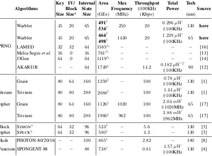
We compare our best results with those of other lightweight primitives (Table 1). We provide the key size, IV/Block size, and internal state size for all the designs, in order to have a fair comparison. From the table, we can see that the areas from both before and after the place and route phase of Warbler are smaller than the estimated areas of LAMED, Melia-Seguiet al.’s PRNG, and J3Gen, and also smaller than the areas of AKARI1B, Grain, Trivium, SIMON, SPECK, PHOTON-80/20/16, and SPONGENT-88. The maximum frequency of Warbler is higher than Grain’s and Trivium’s in CMOS 65nm. The throughput of Warbler is less than that of Grain and Trivium, but greater than that of AKARI1B, SIMON, SPECK, PHOTON-80/20/16, and SPONGENT-88. The total power consumption is related to the operat-ing frequency and the correspondoperat-ing technology. However, as we can see, the total power consumption of Warbler is very small at100KHz, and it is smaller than Grain’s, Trivium’s, and SPONGENT-88’s in CMOS 130nm. Hence, it is very suitable for passive RFID applications. Even though the key size is only 45-bit, Warbler has been proved to be sufficiently secure in the passive RFID tags [11].
This paper is organized as follows. In Section 2, we describe the specification of Warbler. Section 3 first presents our metrics and design flow in CMOS 65nm and CMOS 130nm ASICs. Then, we give our ASIC architecture of Warbler, including the top-level architecture, Finite State Machine (FSM), and datapath. Later, we present our ASIC results and analysis in both CMOS 65nm and CMOS 130nm in Section 4. Finally, Section 5 concludes this paper.
2
Description of Warbler
This section gives a detailed description of Warbler.
2.1 Specification of Warbler
The following terms and notations are used to describe Warbler and its hardware architecture.
– p(x) =x5+x4+x3+x+ 1, a primitive polynomial of degree5over
F2. It is used to generateF25.
Table 1.Comparison of Hardware Implementations of Lightweight Primitives.
Algorithms
Key IV/ Internal Area Max Throughput Total Tech Source Block State Frequency @100KHz Power
Size Size* Size (GEs) (MHz) (Kbps) (nm)
PRNG
Warbler 45 20 65 491
†
250 20 0.296µW 130 here
534‡ @100KHz
Warbler 45 20 65 464
†
1430 20 1.239µW 65 here
498‡ @100KHz
LAMED 32 32 64 15854 − − − − [16]
Melia-Seguiet al. 16 0 16 7614 − − − − [13]
J3Gen 64 0 64 14194 − − − − [14]
AKARI1B − − 64 1749† − 14.2 0.182µW
5
90 [12]
@100KHz
Grain 80 64 160 1259‡ − 100 0.78µW 130 [1]
@100KHz
Stream Trivium 80 80 288 2088‡ − 100 1.44µW 130 [1]
@100KHz
cipher Grain 80 64 160 1126‡ 1020 100 2.04mW 65 [17]
@1020MHz
Trivium 80 80 288 1986‡ 962 100 3.88mW 65 [17]
@962MHz
Block SIMON 64 32 96 523† − 5.6 − 130 [3]
cipher SPECK 64 32 96 580† − 4.2 − 130 [3]
Hash PHOTON-80/20/16 − − 100 865† − 2.82 − 180 [8]
Function SPONGENT-88 − − 88 738† − 0.81 1.57µW 130 [4]
@100KHz *IV is for PRNGs and stream ciphers, and Block is for block ciphers.
†Areas are obtained before the place and route (P & R) phase and‡areas are obtained after the P & R phase.
−The corresponding value is not related or not provided by the authors.
4The estimated area.
5The estimated power consumption in UMC Faraday 90nm library. The smallest one in the SIMONand SPECKfamilies.
– A polynomial basis ofF25 overF2is a basis of the form{1, α, α2, α3, α4}. All the computations in
Warbler are calculated based on this polynomial basis.
– Tr(x) =x+x2+x22+x23+x24, the trace function fromF25 →F2.
– WGP-5(x) =x+ (x+ 1)5+ (x+ 1)13+ (x+ 1)19+ (x+ 1)21,x∈
F25. TheWG-5permutation
fromF25 →F25.
– WGT-5(x) = Tr(WGP-5(x)) = Tr(x19),x∈
F25. TheWG-5transformation with decimation1
fromF25 →F2, which is theWGT2-5module in Figure 1.
– WGT-5(x3) =Tr(WGP-5(x3)) =Tr(x13),x∈
F25. TheWG-5transformation with decimation3
fromF25 →F2, which is theWGT1-5module in Figure 1.
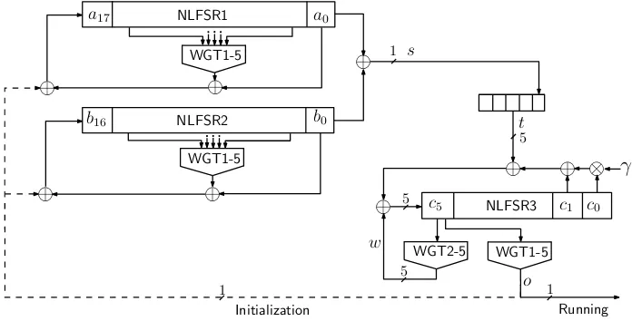
– NLFSR1, a nonlinear feedback shift register with length N1 = 18 and it generates a span N1
sequencea={ai}i≥0, whereai∈F2. Thespan nsequence is a binary sequence with period2n−1
and each non-zero n-tuple occurs exactly once in one period [11].
– NLFSR2, a nonlinear feedback shift register with length N2 = 17 and it generates a span N2
– NLFSR3, a nonlinear feedback shift register with lengthN3 = 6and it generates a sequencec= {ci}i≥0, whereci∈F25.
– g(x) =x6+x+γ, a feedback primitive polynomial of degree6overF25forNLFSR3, andγ=α15.
WGT1-5
a17 a0
b16 b0
WGT1-5 WGT2-5
c5 c0
⊕
⊕
⊕
⊕
⊕
⊕
⊕
c⊕
1γ
1
5
1 5
NLFSR1
NLFSR2
NLFSR3
⊗
WGT1-5Initialization Running
1 s
t
w
o 5
Fig. 1.Key/IV Initialization and Running Phases of Warbler
Warbler is mainly built upon three NLFSRs and fourWG-5 transformation modules. It contains two phases as depicted in Figure 1: the Key and IV initialization phase and the running phase. In the initialization phase, the output of theWGT1-5module inNLFSR3is used to feed back to the inputs of NLFSR1andNLFSR2. The random sequences are generated from the output of theWGT1-5module inNLFSR3in the running phase, and there is no feedback fromWGT1-5module inNLFSR3to the inputs ofNLFSR1andNLFSR2in this phase.
The nonlinear recurrence relations forNLFSR1andNLFSR2without the feedback fromNLFSR3 are defined as follows:
aN1+k=ak⊕WGT-5(x3), x= (ar1+k, ar2+k,· · ·, ar5+k)∈F25.
bN2+k =bk⊕WGT-5(x3), x= (br0
1+k, br
0
2+k,· · ·, br
0
5+k)∈F25. where, k ≥ 0, 0 < ri < N1, and 0 < r
0
i < N2 are the tap positions of NLFSR1 andNLFSR2
respectively. They are listed as below:
(r1, r2, r3, r4, r5) = (4,7,8,10,15),
(r10, r
0
2, r
0
3, r
0
4, r
0
5) = (4,7,8,9,12).
Based on the sequencesa={ai}i≥0andb={bi}i≥0, a new sequences={si|si=ai⊕bi, i≥0} is generated and will be sent to a 5-bit shift register immediately. The element of this 5-bit shift register is used as one feedback forNLFSR3. This element can be represented astk∈F25, k≥0.
The recursive relation forNLFSR3is defined as follows:
cN3+k =γck+ck+1+wk+tk, wk = (0,0,0,0,WGT-5(ck+5)), k≥0,
2.2 The Behaviour of Warbler
Warbler has an internal state of 65 bits: a 45-bit Key (K0, K1, K2,· · · , K44) and a 20-bit IV (IV0, IV1,
IV2,· · ·, IV19). Initially, the Key and IV need to be loaded into the registers inNLFSR1,NLFSR2,
andNLFSR3. The Key bits are loaded into the first consecutive 12, 11, and 22 positions ofNLFSR1, NLFSR2, andNLFSR3respectively. The remaining positions in eachNLFSRare reserved for IV. More Specifically, the Key and IV loading process can be listed as follows.
a11,· · ·, a0=K11,· · · , K0,
a17,· · ·, a12=IV5,· · ·, IV0,
b10,· · ·, b0=K22,· · · , K12,
b16,· · · , b11=IV11,· · ·, IV6,
c0=K27,· · · , K23,
c1=K32,· · · , K28,
c2=K37,· · · , K33,
c3=K42,· · · , K38,
c4=IV14, IV13, IV12, K44, K43,
c5=IV19, IV18, IV17, IV16, IV15.
After we finish loading the Key and IV, a 36-round initialization phase is performed to mix the Key and IV properly. In this phase, the output signalo(Figure 1) from theWGT1-5module inNLFSR3is used as a feedback toNLFSR1andNLFSR2in every clock cycle. The Warbler initialization method is described as follows.
NLFSR1:
x= (ak+4, ak+7, ak+8, ak+10, ak+15),
o0= 0,
ak+18=ak⊕WGT-5(x3)⊕ok, 0≤k≤35.
NLFSR2:
y= (bk+4, bk+7, bk+8, bk+9, bk+12),
o0= 0,
bk+17=bk⊕WGT-5(y3)⊕ok, 0≤k≤35.
5-bit shift register:
sj= 0, j = 0,1,2,3, sk+4=ak⊕bk,
tk= (sk, sk+1, sk+2, sk+3, sk+4), 0≤k≤34.
NLFSR3:
wk= (0,0,0,0,WGT-5(ck+5)),
ck+6=γck+ck+1+wk+tk, ok+1=WGT-5(c3k+5), 0≤k≤34.
The first output sequence bito0fromNLFSR3is manually set to0, which is used for the feedback
fromNLFSR3toNLFSR1andNLFSR2in the first initialization clock cycle. The reason for this setting is that there is a 5-bit shift register betweenNLFSR1andNLFSR2together andNLFSR3.s4needs to
take one clock cycle in order to shift into this 5-bit shift register. Therefore,NLFSR3needs to wait for one clock cycle until the first elementt0in the 5-bit shift register is ready for the feedback computation
ofNLFSR3. As a result, in the initialization phase, theNLFSR1andNLFSR2run for 36 clock cycles, and theNLFSR3runs only for 35 clock cycles.
After theNLFSRsfinish the initialization phase, they simultaneously go to the running phase, where the following 5-bit elementtkis used as a feedback element forNLFSR3.
tkcan be obtained by every five clock cycles from the 5-bit shift register, which results in a1/5(i.e., 1-bit per five clock cycles) throughput of the Warbler output sequenceok+1, k≥35.
3
ASIC Implementation
We discuss the ASIC implementation of Warbler in this section, including the design flow and metrics, and the specific architecture.
3.1 Design Flow and Metrics
We use Synopsys Design Compiler Version D-2010.03-SP4 to synthesize the designs into netlist, based on the STMicroelectronics CMOS 65nm CORE65LPLVT_1.20V and IBM CMOS 130nm CMR8SF-LPLVT Process SAGE v2.0 standard cell library, with both having a typical 1.2V voltage and25◦C temperature. Cadence SoC Encounter v09.12-s159_1 is used to finish the place and route phase in order to generate the layout of the designs. We use Mentor Graphics ModelSim SE 10.1a to conduct functional simulation of the designs and perform timing simulation by using the timing delay information generated from SoC Encounter as well. The area of the design after the logic synthesis is provided for comparisons with previous designs, and a more accurate area after place and route is also provided for deploying the designs in practical cases. The densities used for the place and route phase for CMOS 130nm and 65nm are 0.92 and 0.93 respectively, in order to make a trade-off between area and maximum operating frequency when the densities are pretty high. We choose them because the area after the place and route phase will decrease when the density is higher. However, the corresponding critical path will increase; leading to potential DRC (Design Rule Check) and LVS (Layout Versus Schematic) violations. As usual, the area is measured in gate equivalents (GEs), and one GE is equivalent to the physical area required for the two-input one-output NAND gate with the lowest driving strength of the corresponding technology. The areas of one GE are 2.08(µm)2 and 5.76(µm)2for ST CMOS 65nm and IBM CMOS 130nm
respectively.
We use SoC Encounter v09.12-s159_1 to generate accurate power consumption based on the activity information generated from the timing simulation with a frequency of 100 KHz, and a duration time of 0.1s. We do so because the 100 KHz clock frequency is widely used for benchmarking in resource constrained applications and 0.1s is long enough to provide accurate activity information for all the signals. Moreover, the maximum clock frequency which can be operated for a specific design is obtained by using the critical path after the place and route phase.
In order to be fair enough to compare our results with the related work [3,5,15], we provide the areas of some basic gates in our specific libraries. All the areas of basic gates provided here are the smallest one in the library, and we normalize the two-input one-output NAND gate to be 1. The specific basic gates in our IBM CMOS 130nm and ST CMOS 65nm libraries are listed in Table 2.
Table 2.The Areas of Basic Gates in the Libraries
NAND AND OR NOT XOR XNOR 2-1 MUX DFF 1-bit Full Adder Scan FF
IBM CMOS 130nm 1 1.25 1.25 0.75 2 2 2.25 4.25 5.75 5.5
3.2 ASIC Architecture
In this subsection, we target a low-area implementation of Warbler but still maintain a very high max-imum operating frequency. We first provide the top-level architecture of Warbler and then present the architectures of FSM and datapath.
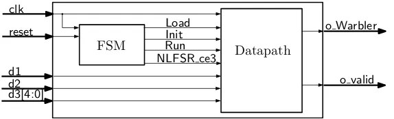
Entire Architecture
We provide a top-level architecture for Warbler in Figure 2, and the entire architecture includes two parts: FSM and datapath. FSM is used to provide state transition signals (Load,Init,Run) and the register chip-enable signal (NLFSR_ce3) for the datapath. The datapath is used to load the initial data for the registers (Section 2.2) using the input ports (d1,d2,d3), to process the internal sates in the registers, and then to output the sequence (o_Warbler) and the valid signal (o_valid).
FSM Datapath
clk reset
d1 d2
o Warbler
o valid d3[4:0]
Init Load
NLFSR ce3Run
Fig. 2.The Top-level Architecture of Warbler
FSM
Our architecture has three states:loading,initialization, andrunning. Theloadingstate takes18 clock cycles, theinitializationstate lasts for36clock cycles, and therunningstate lasts forever unless Warbler is reset. Specifically, our FSM goes intoloadingstate immediately whenresetequals1. Warbler reads the initial data fromd1into the datapath onceresetgoes to0again, and it reads data fromd2and data fromd3in the2th and13th clock cycles of theloadingstate respectively. Once theloadingstate is finished, theinitializationandrunningstates will run.
From the description of Warbler in Section 2, we know that the throughput of Warbler is1/5, because theShift5module takes five clock cycles for one feedback computation ofNLFSR3in therunningstate. Therefore, a register chip-enable signal (NLFSR_ce3) is required to controlNLFSR3in order to output the sequence correctly. However,NLFSR1andNLFSR2 always run afterreset, which makes them use only the standard registers without chip-enable signals. This property reduces the Warbler’s area. Furthermore, it also explains why we have only one chip-enable signal in our architecture in Figure 2.
Recently, LFSR based counters have been used to replace the binary counter in the FSM in hardware implementations [10], because they only contain several registers and some combinational feedback logic without using a full-adder. In general, the combinational logic of the LFSR counter is smaller than the full-adder of the binary counter in terms of area. Therefore, we can achieve some hardware benefits by using the LFSR counter to replace the binary counter. The binary and LFSR counter-based designs are both provided in this paper. To design our LFSR counter, we use a primitive polynomial (X6+X+ 1)
with an initial value (1, 1, 1, 1, 1, 1).
from63in each state for the LFSR counter-based design. The states transition conditions for these two designs are summarized in Table 3. TheLoadsignal stays at1 when the FSM is in theloadingstate; otherwise, it equals0. The similar case for theInitandRunsignals.
Table 3.States Transition Conditions for FSM
States Binary counter-based LFSR counter-based
Loading (100)→initialization (010) 17 17
Initialization (010)→running (001) 35 39
The chip-enable signal (NLFSR_ce3) is generated as follows: it is set to1in theloadingstate,1 in theinitializationstate except the first clock cycle, and(0,0,0,0,1)in every five clock cycles in the runningstate.
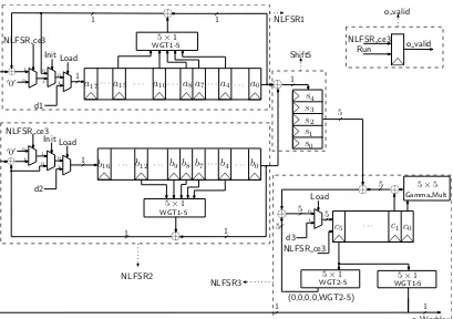
Datapath
The datapath for Warbler in our ASIC architecture is shown in Figure 3. It includes five parts: NLFSR1,NLFSR2,NLFSR3,Shift5, ando_valid.NLFSR1contains a 18-stage register, aWGT1-5 module, and other feedback logic. Similarly,NLFSR2contains a 17-stage register, aWGT1-5module, and other feedback logic.NLFSR3contains a 6-stage register, aGamma_Multmodule, a WGT1-5 module, aWGT2-5module, and other feedback logic.Shift5is used for the 5-bit shift register and is comprised of a 5-stage register and other combinational logic. Moreover,o_validprovides a valid signal for the Warbler output sequence.
According to Section 2.2, the feedback values vary for different states. Therefore,Init,Load, and NLFSR_ce3are used to select correct feedback values for NLFSRsin each state. Furthermore, the NLFSR_ce3is used to control the throughput of output sequence (o_Warbler) and the output valid signal (o_valid). The datapath works with the FSM together to generate a pseudorandom sequence cor-rectly.
The Gamma_Multmodule is used for the calculation of γck inF25. Under the polynomial basis representation, the elementX ∈F25 (X =x0+x1α+x2α2+x3α3+x4α4) multiplied byγ=α15
can be computed as follows:
X·α15= (x0+x1α+x2α2+x3α3+x4α4)·α15
=x0α15+x1α16+x2α17+x3α18+x4α19
= (x2+x4) + (x2+x3+x4)α+ (x0+x3+x4)α2+
(x0+x1+x2)α3+ (x1+x3+x4)α4.
Therefore, the result ofX·γis represented as a5-bit vector(x2⊕x4, x2⊕x3⊕x4, x0⊕x3⊕x4, x0⊕
x1⊕x2, x1⊕x3⊕x4). Thus, we can implement ourGamama_Multmodule using the finite field logic
directly.
Similarly, we can computeWGT-5(x3)andWGT-5(x)in polynomial basis for everyx ∈
F25 by
using the finite field logic directly or pre-storing them to two look-up tables (WGT1-5andWGT2-5 re-spectively), as in [17]. However, the hardware implementations ofWGT1-5module (with decimation 3) andWGT2-5module (with decimation 1) are more efficient if the look-up table method?is used rather than the finite field logic methods [17]. Therefore, we use the look-up table methods for implementing theWGT1-5andWGT2-5modules.
?
a17 a0
WGT1-5
⊕
5×1
a4
Shift5
a7
a8
a10
a15 · · · ·
· · ·
b16 · · · b12 · · · b9 b8 b7· · ·b4 · · · b0
Load Init NLFSR ce3 d1 0 1 0 1 0 1 000 ⊕ Load Init NLFSR ce3 d2 0 1 1 0 0 1 000 ⊕
WGT1-55×1
⊕
⊕
s0 s1 s2 s3 s4 c0 c1c5 · · ·
⊕
⊕
5
Gamma Mult5×5
5 d3
⊕
Load NLFSR ce3 1 0WGT1-55×1 WGT2-55×1
(0,0,0,0,WGT2-5) 5 o valid NLFSR ce3 o Warbler 1 1 1 1 1 1
1 NLFSR1 o valid
NLFSR2 NLFSR3 Run 5 5 1 1
Fig. 3.Datapath of Warbler
4
ASIC Results and Analysis
In this section, we first give the ASIC implementation results of Warbler, using our architecture in CMOS 65nm and CMOS 130nm. Then, we provide a comprehensive analysis of the area that use different technologies and various compilation techniques.
4.1 ASIC Results
We use three different compilation techniques in Design Compiler to perform hardware optimizations: simple compile, compile ultra, and compile ultra with clock gating. The simple compile options can provide us with the hierarchal architectures of the design, and the area of specific submodules. The compile ultra option can make deeper optimizations by optimizing the entire module together, thereby reducing the area and power consumption significantly [5,10] . The clock gating technique can further reduce the area and power consumption [5].
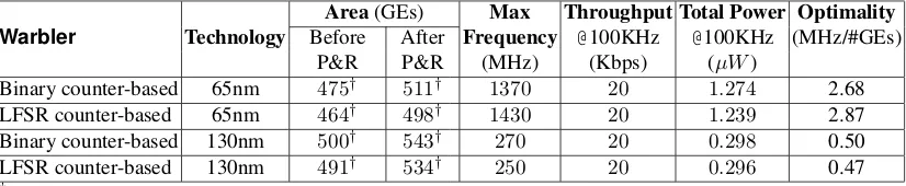
Table 4.Our ASIC Implementation Results of Warbler in CMOS 65nm and CMOS 130nm.
Warbler Technology
Area(GEs) Max Throughput Total Power Optimality
Before After Frequency @100KHz @100KHz (MHz/#GEs) P&R P&R (MHz) (Kbps) (µW)
Binary counter-based 65nm 475† 511† 1370 20 1.274 2.68
LFSR counter-based 65nm 464† 498† 1430 20 1.239 2.87
Binary counter-based 130nm 500† 543† 270 20 0.298 0.50
LFSR counter-based 130nm 491† 534† 250 20 0.296 0.47
†Area obtained by using compile ultra and clock gating techniques.
techniques with a purpose of comparison with other designs. The corresponding maximum frequency is given by using the critical path. The throughput of Warbler is1/5, as mentioned in Section 2. Therefore, it is20Kbps at 100 KHz, the typical frequency for benchmarking lightweight primitives. Similarly, the total power consumption is provided at 100 KHz. Since the operating frequency is so small, the static power consumption dominates the total power consumption. However, the static power consumption is larger in CMOS 65nm than in CMOS 130nm. Therefore, the total power consumption of Warbler in CMOS 65nm is larger than in CMOS 130nm. In addition, the maximum frequency and total power consumption are both obtained after the place and router phase in order to be closer to the practical cases. The optimality is given based on our trade-off strategy.
From Table 4, we can see that the LFSR based design is smaller than the binary counter-based design (i.e.,11GEs and9GEs smaller in CMOS 65nm and CMOS 130nm respectively, for the areas before the place and route). Similarly, the total power consumption of the LFSR counter-based design is smaller than that of the binary counter-based design in both CMOS 65nm and CMOS 130 nm. The optimality for the LFSR counter-based design is higher than that for the binary counter-based design in CMOS 65nm, but opposite in CMOS 130nm.
Our another observation is that the sequential logic dominates the entire area. In the area before the place and route phase, for example, the proportion of sequential logic (Table 5), depends on the adopted technologies and compilation techniques. However, they are all above 65%.
Table 5.The Sequential Logic Ratios of Warbler
Warbler
CMOS 65nm CMOS 130nm
Compile Compile Compile ultra Compile Compile Compile ultra simple ultra + clock gating simple ultra + clock gating Binary counter-based 65.0% 66.7% 65.0% 70.0% 71.5% 72.4% LFSR counter-based 65.6% 67.4% 66.7% 71.3% 73.2% 73.4%
4.2 Results Analysis
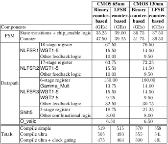
In order to thoroughly analyze the constitution of the area of Warbler in CMOS 65nm and CMOS 130nm, we break down the entire area from before the place and route phase into separate submodules, as shown in Table 6. It is worth noting that the following analysis is based on the areas of the submodules which are obtained by using the compile simple technique.
Table 6.Breakdown of the Implementation Results of Warbler before the Place and Route Phase
CMOS 65nm CMOS 130nm Binary LFSR Binary LFSR
counter-based based based based
Components (GEs) (GEs) (GEs) (GEs)
FSM State transitions + chip_enable logic 35.25 39.00 36.75 37.50
Counter 47.50 39.25 51.75 39.50
Datapath
NLFSR1
18-stage register 67.50 76.50
WGT1-5 15.50 14.50
Other feedback logic 10.00 9.50
NLFSR2
17-stage register 63.75 72.25
WGT1-5 15.50 14.50
Other feedback logic 10.00 9.50
NLFSR3
6-stage register 150.00 180.00
Gamma_Mult 13.75 14.00
WGT1-5 15.50 14.50
WGT2-5 9.25 9.50
Other feedback logic 32.50 30.75
Shift5 5-stage register 18.75 21.25
Other combinational logic 8.00 8.00
O_valid 6.50 6.50
Compile simple 519 515 570 558
Totals Compile ultra 505 493 555 541
Compile ultra + clock gating 475 464 500 491
are only 5.5% and 13% smaller accordingly, due to the area of state transitions and chip-enable logic is bigger in the LFSR counter-based FSM than in the binary counter-based FSM.
For the registers inNLFSR1,NLFSR2, andShift5, we can verify that they are indeed implemented by the standard registers without chip-enable signals. For example, the area of this type of register in CMOS 65nm is 3.75 GEs (Table 2), and the total area is 67.50 GEs for the 18-stage register inNLFSR1. This area is confirmed with our architecture as described in Section 3.2. The areas of combinational logic, such as theWGT1-5module, depend on the areas of basic gates in the different technologies. For example, the areas of theWGT1-5module are 15.50 GEs and 14.50 GEs in CMOS 65nm and CMOS 130nm respectively. The same situation exists for other submodules.
For the area of NLFSR3, the 6-stage register use registers with chip-enables, and moreover the WGT1-5 andWGT2-5 modules are different in the same technology (i.e., 15.50 GEs and 9.25 GEs respectively in CMOS 65nm, and 14.50 GEs and 9.50 GEs respectively in CMOS 130nm). We give the specific contents of these two look-up tables in Table 7. As we can see, the position distributions of1 and0 are different for theWGT1-5 andWGT2-5 modules, and they are computed based onWG-5 transforms with decimation3and1respectively. The synthesis tool is able to optimizeWGT2-5to the simpler logic in hardware thanWGT1-5; therefore, the area ofWGT1-5is bigger thanWGT2-5’s as shown in Table 6. The distinct areas of differentWG-5transformation tables give us the worthwhile idea to select a decimation value in order to make theWG-5transformation table as small as possible for a new design.
Table 7. TheWGT1-5andWGT2-5Look-up Tables
Address 0 1 2 3 4 5 6 7 8 9 10 11 12 13 14 15 16 17 18 19 20 21 22 23 24 25 26 27 28 29 30 31 WGT1-50 0 1 0 0 1 1 1 0 1 1 1 1 0 0 0 1 0 1 0 0 0 1 1 0 1 1 0 0 1 0 1 WGT2-50 0 0 0 0 1 0 0 0 0 0 1 1 1 1 1 1 1 0 1 1 1 0 0 1 0 0 1 1 1 0 1
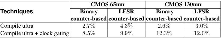
can reduce the area by at least2.6%, and compile ultra plus clock gating can reduce the area by at least
8.5%for our Warbler designs.
Table 8.The Area Reduction Percentages by using Compile Ultra and Compile Ultra plus Clock Gating
Techniques
CMOS 65nm CMOS 130nm
Binary LFSR Binary LFSR
counter-based counter-based counter-based counter-based
Compile ultra 2.7% 4.3% 2.6% 3.0%
Compile ultra + clock gating 8.5% 9.9% 12.3% 12.0%
5
Concluding Remarks
In this paper, we have presented hardware implementations of Warbler in CMOS 65nm and CMOS 130nm ASICs. We proposed an architecture that takes advantage of standard registers without chip-enable signals. In addition, we investigated two methods for designing theFSM: binary counter-based and LFSR counter-based. We used three different compilation techniques to optimize our designs. We can achieve the areas of 498 GEs and 534 GEs after the place and route phase in CMOS 65nm and CMOS 130nm respectively. The corresponding maximum frequencies are 1430 MHz and 250 MHz respectively, for CMOS 65nm and CMOS 130nm. The power consumption of Warbler is very small at 100 KHz: only 1.239µW and 0.296µW respectively, for CMOS 65nm and CMOS 130nm. From the ASIC results, we have determined that the LFSR based design is better than the binary counter-based design in terms of smaller area and lower total power consumption. In addition, the sequential logic ratios for all our designs are larger than 65% for both CMOS 65nm and CMOS 130nm. Our analysis has verified that the areas of NLFSRs and combinational logic are dependent upon the type of registers and the adopted technologies. The area of theWG-5 transformation table depends upon the selected decimation value, giving us some suggestions for future ciphers and pseudorandom number generator designs usingWG-5transformations. When compared with other lightweight primitives, the area of our Warbler implementation is smaller than the estimated areas of LAMED, Melia-Segui et al.’s PRNG, and J3Gen, and also smaller than the areas of AKARI1B, Grain, Trivium, SIMON, SPECK, PHOTON-80/20/16, and SPONGENT-88. In conclusion, Warbler can fit into passive RFID systems.
References
3. R. Beaulieu, D. Shors, J. Smith, S. Treatman-Clark, B. Weeks, and L. Wingers. The SIMON and SPECK Fam-ilies of Lightweight Block Ciphers. Cryptology ePrint Archive, Report 2013/404, 2013. http://eprint. iacr.org/.
4. A. Bogdanov, M. Kneževi´c, G. Leander, D. Toz, K. Varıcı, and I. Verbauwhede. SPONGENT: A Lightweight Hash Function. InCryptographic Hardware and Embedded Systems–CHES 2011, pages 312–325. Springer, 2011.
5. C. De Canniere, O. Dunkelman, and M. Kneževi´c. KATAN and KTANTAN: A Family of Small and Efficient Hardware-oriented Block Ciphers. InCryptographic Hardware and Embedded Systems-CHES 2009, pages 272–288. Springer, 2009.
6. D. Engels, X. Fan, G. Gong, H. Hu, and E. M. Smith. Ultra-lightweight Cryptography for Low-cost RFID Tags: Hummingbird Algorithm and Protocol.Centre for Applied Cryptographic Research (CACR) Technical Reports, 29, 2009.
7. EPCglobal. EPC Radio Frequency Identity Protocols Class-1 Generation-2 UHF RFID Protocol for Communi-cations at 860 MHZ - 960 MHz.http://www.gs1.org/sites/default/files/docs/uhfc1g2/ uhfc1g2_2_0_0_standard_20131101.pdf, 2013.
8. J. Guo, T. Peyrin, and A. Poschmann. The PHOTON Family of Lightweight Hash Functions. InAdvances in Cryptology–CRYPTO 2011, pages 222–239. Springer, 2011.
9. A. Juels and S. A. Weis. Authenticating Pervasive Devices with Human Protocols. InAdvances in Cryptology– CRYPTO 2005, pages 293–308. Springer, 2005.
10. L. Knudsen, G. Leander, A. Poschmann, and M. J. Robshaw. PRINTcipher: A Block Cipher for IC-printing. In
Cryptographic Hardware and Embedded Systems, CHES 2010, pages 16–32. Springer, 2010.
11. K. Mandal, X. Fan, and G. Gong. Warbler: A Lightweight Pseudorandom Number Generator for EPC C1 Gen2 Tags. InRadio Frequency Identification System Security: RFIDsec’12 Asia Workshop Proceedings, page 73. IOS Press, 2013.
12. H. Martin, E. San Millán, P. Peris-Lopez, and J. E. Tapiador. Efficient ASIC Implementation and Analysis of Two EPC C1 G2 RFID Authentication Protocols.Sensors Journal, IEEE, 13(10):3537–3547, 2013.
13. J. Melia-Segui, J. Garcia-Alfaro, and J. Herrera-Joancomarti. Analysis and Improvement of a Pseudorandom Number Generator for EPC Gen2 Tags. InFinancial Cryptography and Data Security, pages 34–46. Springer, 2010.
14. J. Melià-Seguí, J. Garcia-Alfaro, and J. Herrera-Joancomartí. J3Gen: A PRNG for Low-cost Passive RFID.
Sensors, 13(3):3816–3830, 2013.
15. A. Moradi, A. Poschmann, S. Ling, C. Paar, and H. Wang. Pushing the Limits: A Very Compact and a Threshold Implementation of AES. InAdvances in Cryptology–EUROCRYPT 2011, pages 69–88. Springer, 2011. 16. P. Peris-Lopez, J. C. Hernandez-Castro, J. M. Estevez-Tapiador, and A. Ribagorda. LAMED–A PRNG for EPC
Class-1 Generation-2 RFID Specification.Computer Standards & Interfaces, 31(1):88–97, 2009.