Survey of Matrix Multiplication using IEEE
754 Floating Point for Digital Image
Compression
Sandhya Rai
1, Prof. Suresh. S. Gawande
2M. Tech. Scholar, Department of Electronics and Communication, Bhabha Engineering Research Institute, Bhopal, India1
Head of Department, Department of Electronics and Communication, Bhabha Engineering Research Institute, Bhopal, India 2
ABSTRACT: Due to advancement of new technology in the field of VLSI and Embedded system, there is an increasing demand of high speed and low power consumption processor. Speed of processor greatly depends on its multiplier as well as adder performance. In spite of complexity involved in floating point arithmetic, its implementation is increasing day by day. Due to which high speed adder architecture become important. Several adder architecture designs have been developed to increase the efficiency of the adder. In this paper, we introduce an architecture that studied of matrix multiplication using IEEE 754 floating point multiplier and different types of adder.
KEYWORDS: IEEE 754, Single Precision Floating Point (SPFP), Double Precision Floating Point (DPFP)
I. INTRODUCTION
Matrix multiplication is commonly used in most signal processing algorithms. It is also a frequently used kernel operation in a wide variety of graphics, image processing as well as robotic applications. The matrix multiplication operation involves a large number of multiplication as well as accumulation. Multipliers have large area, longer latency and consume considerable power compared to adders. Registers, which are required to store the intermediate product values, are also major power intensive component [1]. These components pose a major challenge for designing VLSI structures for large-order matrix multipliers with optimized speed and chip-area. However, area, speed and power are usually conflicting hardware constraints such that improving upon one factor degrades the other two [2].
The real numbers represented in binary format are known as floating point numbers. Based on IEEE-754 standard, floating point formats are classified into binary and decimal interchange formats. Floating point multipliers are very important in dsp applications. This paper focuses on double precision normalized binary interchange format. Figure 1 shows the IEEE-754 double precision binary format representation. Sign (s) is represented with one bit, exponent (e) and fraction (m or mantissa) are represented with eleven and fifty two bits respectively. For a number is said to be a normalized number, it must consist of'one' in the MSB of the significand and exponent is greater than zero and smaller than 1023. The real number is represented by equations (i) & (2).
Z
(
1
s)
2
(EBias)
(
1
.
M
)
(1)Biasing makes the values of exponents within an unsigned range suitable for high speed comparison.
IEEE 754 standard floating point multiplication algorithm
A brief overview of floating point multiplication has been explained below [3-4].
Both sign bits S1, S2 are need to be Xoring together, then the result will be sign bit of the final product. Both the exponent bits E1, E2 are added together, then subtract bias value from it. So, we get exponent field of
the final product.
Significand bits Sig1 and Sig2 of both the operands are multiply including their hidden bits.
Normalize the product found in step 3 and change the exponent accordingly. After normalization, the leading “1 “will become the hidden bit.
Above algorithm of multiplication algorithm is shown in Figure 2.
Sign Bit Significand Biased Exponent Si
1-bit 8/11-bit 23/52-bit
Figure 1: IEEE 754 Single Precision and Double Precision Floating Point Format
E
2 E
1
XOR S1 S2
Sig1 Sig2
- Bias
X3=X1*X2
S3 E Sig3 3
NE NS
Soumya Havaldar et al. [2], gives an FPGA Based High Speed IEEE-754 Double Precision Floating Point Multiplier Using Verilog. This paper has implemented DPFP Multiplier using parallel Adder. A high speed floating point double precision multiplier is implemented on a Virtex-6 FPGA. In addition, the proposed design is compliant with IEEE-754 format and handles over flow, under flow, rounding and various exception conditions. The design achieved the operating frequency of 414.714 MHz with an area of 648 slices.
Ragini Parte et al. [3], IEEE point number-crunching has an immense application in DSP, advanced PCs, robots because of its capacity to speak to little numbers and huge numbers and in addition marked numbers and unsigned numbers. Disregarding unpredictability included in gliding point number juggling, its usage is expanding step by step. Here we break down the impacts of utilizing three unique sorts of adders while figuring the single accuracy and twofold exactness skimming point increase. We additionally exhibit the increase of significand bits by disintegration of operands strategy for IEEE 754 standard.
Ross Thompson et al. [4], IEEE-754 determines trade and number juggling positions also, routines for paired and decimal drifting point number juggling in PC programming world. The execution of a skimming point framework utilizing this standard should possible completely in programming, or in equipment, or in any blend of programming and equipment. This venture propose VHDL execution of IEEE - 754 Floating point unit .In proposed work the pack, unload and adjusting mode was actualized utilizing the VHDL dialect and reenactment was checked.
In this proposition work, DPFP Multiplier alongside SPFP Multiplier has been actualized with four ordinary Adders (PA, CSKA, CSA, and CSABEC). Think about their Results and CSA is known not the speediest snake among every single customary viper. Be that as it may, CSA involves more territory as it has two parallel circuits to include the same bits yet with diverse convey data. As CSA figures the whole without sitting tight for the transitional conveys to spread stage by stage. Finally it is the obligation of multiplexer to pick and give the last right yield. CSABEC is an adjusted adaptation of CSA in which one of the parallel circuits is supplanted by the arrangement of Binary to Excess-1 Converters circuit (BECs). It is turned out to be an awesome way to deal with decrease the territory.
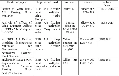
Table 1: Summary of Literature Review
Entitle of paper Approached used Software Parameter Published Year Design of Vedic IEEE
754 Floating Point Multiplier
IEEE 754 floating point multiplier
using Vedic
Multiplier
Xilinx 12.1 i
Slice = 305, LUT= 598
IEEE 2016
Analysis of Effects of using Exponent Adders in IEEE- 754 Multiplier by VHDL
IEEE 754 floating point multiplier using Carry select adder
Verilog using the Model SIM
SE 6.3
Slice = 353, LUT= 610
IEEE 2015
An IEEE 754 Double-Precision Floating-Point
Multiplier for
Denormalized and
Normalized Floating-Point Numbers
IEEE 754 floating point multiplier using floating number
Xilinx Spartan 3E xa3s250e- 4vqg100
Slice = 453, LUT= 678
IEEE 2015
High Performance FPGA Implementation of
Double Precision
Floating Point
Adder/Subtractor
IEEE 754 floating point multiplier using adder and sub-tractor
Xilinx ISE 12.2
Slice = 543, LUT= 792
IEEE 2011
III. DIFFERENT TYPES OF ADDER
Parallel Adder:-
Figure 4: Modified Parallel Adder (n=7 for SPFP and n=10 for DPFP)
Carry Skip Adder:-
This adder gives the advantage of less delay over Ripple carry adder. It uses the logic of carry skip, i.e. any desired carry can skip any number of adder stages. Here carry skip logic circuitry uses two gates namely “and gate” and “or gate”. Due to this fact that carry need not to ripple through each stage. It gives improved delay parameter. It is also known as Carry bypass adder. Generalized figure of Carry Skip Adder is shown in figure 5.
Figure 5: Carry Skip Adder
Carry Select Adder:-
Carry select adder uses multiplexer along with RCAs in which the carry is used as a select input to choose the correct output sum bits as well as carry bit. Due to this, it is called Carry select adder. In this adder two RCAs are used to calculate the sum bits simultaneously for the same bits assuming two different carry inputs i.e. „1‟ and „0‟. It is the responsibility of multiplexer to choose correct output bits out of the two, once the correct carry input is known to it. Multiplexer delay is included in this adder. Generalized figure of Carry select adder is shown in figure 3.9. Adders are the basic building blocks of most of the ALUs (Arithmetic logic units) used in Digital signal processing and various other applications. Many types of adders are available in today‟s scenario and many more are developing day by day.
Figure 6: Carry Select Adder
IV.PROPOSED DESIGN
In IEEE754 standard floating point representation, 8 bit Exponent field in single precision floating point (SP FP) representation and 11 bit in double precision floating point (DP FP) representation are need to add with another 8 bit exponent and 11 bit exponent respectively, in order to multiply floating point numbers represented in IEEE 754 standard as explained earlier. Ragini et al. [10] has used parallel adder for adding exponent bits in floating point multiplication algorithm. We proposed the use of 8-bit modified CSA with dual RCA and 8-bit modified CSA with RCA and BEC for adding the exponent bits. We have found the improved area of 8-bit modified Carry select adder with RCA and BEC over the 8-bit modified CSA with dual RCA.
o Sign bit calculation
To calculate the sign bit of the resultant product for SP FP and DP FP multiplier, the same strategy will work. We just need to XOR together the sign bits of both the operands. If the resultant bit is „1‟, then the final product will be a negative number. If the resultant bit is „0‟, then the final product will be a positive number.
o Exponent bit calculation
Add the exponent bits of both the operands together, and then the bias value (127 for SPFP and 1023 for DPFP) is subtracted from the result of addition. This result may not be the exponent bits of the final product. After the significand multiplication, normalization has to be done for it. According to the normalized value, exponents need to be adjusted. Theadjusted exponent will be the exponent bits of the final product.
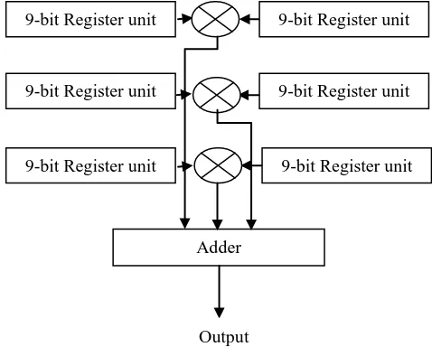
9-bit Register unit 9-bit Register unit
9-bit Register unit 9-bit Register unit
9-bit Register unit 9-bit Register unit
Adder
Output
Matrix Multiplication
In this design we have reduced the resource utilization in terms of number of multipliers and registers in lieu of the completion time.
This design is particularly useful where resources are limited and design can be compromised on basis of increased completion time. The basic working model for a 3 × 3 matrix-matrix multiplication is shown in figure 7 below.
Considering the matrix – matrix multiplication of two n×n matrices, the calculation is performed using n number of
multipliers, n number of registers and n-1 number of adders.
n
2cycles are required to perform the matrix multiplication operation. Each multiplier has two input ports: one each from matrix A and B. In each cycle, n numbers of multiplications are performed and the products are fed to the adder block to give a single element of the outputmatrix, C. The data flow to the multipliers are such that,
k
thmultiplier is fed fromk
th column of matrix A and thk
row of matrix B, where 1 < k < n. At thek
thmultiplier, each element from matrix A is repeated for n consecutive cycles whereas the elements from matrix B are cycled back after n cycles. The partial products are then fed to the adder which computes the final result.For a better understanding of the process, let us consider the matrix multiplication for n = 3 (as shown in figure 1). In this case, 3 multipliers and 3 registers are used to calculate and store the partial products respectively. These partial products are then fed to the adder block to compute the final result. The first multiplier receives input from the first column of matrix A (ak1) and first row of matrix B (b1k), where. Each element of the matrix A at the first multiplier is
repeated for 3 cycles, such that the data flow can be represented as
a
11a
11a
11a
21a
21a
21a
31a
31a
31.Similarly, at thefirst multiplier, the elements of B are repeated after 3 cycles, such that the input data-flow will be
13 12 11
b
b
b
b
11b
12b
13b
11b
12b
13. The other two multipliers receive the component of A and B in the similar order as the first multiplier. After the multiplication, the partial products are fed to the adder which computes the elements of outputmatrix C in row major order given by
c
11c
12c
13c
21c
22c
23c
31c
32c
33. So the entire matrix multiplication operation isperformed in
n
2=9 cycles.V.CONCLUSION
IEEE754 standardize two basic formats for representing floating point numbers namely, single precision floating point and double precision floating point. Floating point arithmetic has vast applications in many areas like robotics and DSP. Delay provided and area required by hardware are the two key factors which are need to be consider Here we present single precision floating point multiplier by using two different adders namely modified CSA with dual RCA and modified CSA with RCA and BEC.
Among all two adders, modified CSA with RCA and BEC is the least amount of Maximum combinational path delay (MCDP). Also, it takes least number of slices i.e. occupy least area among all two adders.
REFERENCES
[1] Lakshmi kiran Mukkara and K.Venkata Ramanaiah, “A Simple Novel Floating Point Matrix Multiplier VLSI Architecture for Digital Image
Compression Applications”, 2nd International Conference on Inventive Communication and Computational Technologies (ICICCT 2018) IEEE.
[2] Soumya Havaldar, K S Gurumurthy, “Design of Vedic IEEE 754 Floating Point Multiplier”, IEEE International Conference On Recent Trends
In Electronics Information Communication Technology, May 20-21, 2016, India.
[3] Ragini Parte and Jitendra Jain, “Analysis of Effects of using Exponent Adders in IEEE- 754 Multiplier by VHDL”, 2015 International
Conference on Circuit, Power and Computing Technologies [ICCPCT] 978-1-4799-7074-2/15/$31.00 ©2015 IEEE.
[4] Ross Thompson and James E. Stine, “An IEEE 754 Double-Precision Point Multiplier for Denormalized and Normalized
Floating-Point Numbers”, International conference on IEEE 2015.
[5] M. K. Jaiswal and R. C. C. Cheung, “High Performance FPGA Implementation of Double Precision Floating Point Adder/Subtractor”, in
International Journal of Hybrid Information Technology, vol. 4, no. 4, (2011) October.
[6] B. Fagin and C. Renard, "Field Programmable Gate Arrays and Floating Point Arithmetic," IEEE Transactions on VLS1, vol. 2, no. 3, pp.
[7] N. Shirazi, A. Walters, and P. Athanas, "Quantitative Analysis of Floating Point Arithmetic on FPGA Based Custom Computing Machines," Proceedings of the IEEE Symposium on FPGAs for Custom Computing Machines (FCCM"95), pp.155-162, 1995.
[8] Malik and S. -B. Ko, “A Study on the Floating-Point Adder in FPGAs”, in Canadian Conference on Electrical and Computer Engineering
(CCECE-06), (2006) May, pp. 86–89.
[9] D. Sangwan and M. K. Yadav, “Design and Implementation of Adder/Subtractor and Multiplication Units for Floating-Point Arithmetic”, in
International Journal of Electronics Engineering, (2010), pp. 197-203.
[10] L. Louca, T. A. Cook and W. H. Johnson, “Implementation of IEEE Single Precision Floating Point Addition and Multiplication on FPGAs”,
Proceedings of 83rd IEEE Symposium on FPGAs for Custom Computing Machines (FCCM‟96), (1996), pp. 107–116.
[11] Jaenicke and W. Luk, "Parameterized Floating-Point Arithmetic on FPGAs", Proc. of IEEE ICASSP, vol. 2, (2001), pp. 897-900.
[12] Lee and N. Burgess, “Parameterisable Floating-point Operations on FPGA”, Conference Record of the Thirty-Sixth Asilomar Conference on
Signals, Systems, and Computers, (2002).
[13] M. Al-Ashrafy, A. Salem, W. Anis, “An Efficient Implementation of Floating Point Multiplier”, Saudi International Electronics,