Effect of Etching Time on Electrical Properties
for Porous Silicon by Photo Electrochemical Etching
Ayad Zwayen Mohammed, Marwa s. Alwazny, Qamer Qasem
University Of Technology, Bahgdad, Iraq
1. Abstract
in this study laser with 532 nm wavelength is used to illuminate silicon wafers dip in HF solution, These wafers are etched at different illumination times (5 -25) min. PSi/c-Si structure is obtain to formed
heterojunction. Study its electrical characteristics such as
current density – voltage (J-V) and capacitance voltage (C-V), then calculate and find the ideality factor which ranged between (6.5-7.03), and built in potential.
Key word; photo-electrochemical etching; porous silicon; morphological properties; electrical properties
Introduction
Over many years PSi attracted attention of researchers to investigate its different properties, due to its use in many industrial and science areas specially its photoluminescence (PL) property at room temperature and developing PS based devices [1,2], such as optical
devices [3], sensors [4] and optoelectronic light-emitting devices [5]. Structurally, PS is very complicated. Some published papers indicate that PS layers consist of Si columns and pores or isolated nanocrystallites [6]. On the other hand, PS may be considered as a system of interconnected quantum wells, the so-called quantum sponge [7]. Due to this interesting
structure of PSi and in order to integrate PS into electronic circuits or to develop PS based devices, the electrical properties of this material must
be studied thoroughly. It is a difficult case because this material has a very irregular surface topography, which causes instabilities in PS-based devices [8]. Thus one must study the electrical properties of devices
prepared at different preparation conditions. In this research we change
the time of etching and study its effect on the electrical properties PS /C-Si junction
2. Experimental work
The substrate used in this experiment is n-type silicon wafer with orientation of (100). Wafers were cleaned to remove any oxide layer formed on the Si substrate when etched with cleaning solution consisting of (HNOR3R, CH R3RCOOH, HF) at ratios (2:1:1:10) [9], to remove oxides by
placing wafers in the ultrasonic machine (Cerry PUL 125 device) for 15
minutes, then cleaning them by alcohol and ultrasonic machine for 15 minutes, then finally cleaned by water and ultrasonic waves for another 15 minutes.
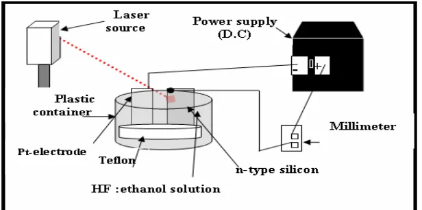
PS layers were fabricated using photo electrochemical method, by
dipping Si wafer in (40%) concentration HF solution, then illuminated with diode laser of 532 nm wavelength and 20 mW power density at different etching times of (5, 10, 15, 20, 25) min. Figure (1) shows the scheme for photo electrochemical (PEC) method [10]
Figure (1): Scheme of PEC method
Electrical properties of the formed heterojunction were measured
for forward and reverse current under dark condition. C-V characteristics of the junction under test were measured using a PM6306 programmable LRC meter supplied by Fluke. The reverse bias voltage ranged through (0.1-1.2) V. The cross point (1/CP
2
P
=0) of the (1/CP 2
P
-V) curve represents the built-in potential of the junction [11]
The characterization of current voltage under dark condition was used to determine the ideality factor (η) which is calculated by the following equations (1) [12].
s
I I V kT
q
ln
∆ ⋅ =
η (1)
Where IS is the saturation current density.
3. Result and discussion
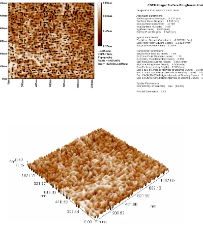
Surface morphology of porous sample shown in Figure (2), where it
depicts the correlation of the average pore diameter as well as the pore
density of the PS at 20 min etching time. Result exhibit the uniform wall etching porous silicon from bulk silicon with average pore diameter was 29.06 nm (meso porous) with root mean square (roughness) 0.139 nm.
Figure (2) surface morphology of silicon porous layer
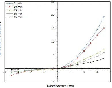
Generally the forward current in Figure (2) shows the presence of two distinguished regions. First, at low voltage (VRFR < 3kT/q), the
recombination current is dominant, because the concentration of charge carriers is greater than the concentration of charge intrinsic (np > niP
2
P
).
Therefore, for equilibrium case, recombination process will take place. This means that each excited electron from valence band to conduction band will recombine with a hole in valence band. Second, at high voltage
(VRFR > 3KT/q), the forward current increases exponentially because the
bias voltage potential exceeds the potential barrier.
In the reverse current, there are two regions; one at low voltage, where the current increases with the applied voltage and the generating
current is dominant. In the second region, the current is dependent on voltage and the diffusion current
After dividing the forward and reverse current to specific regions, one can notice the decreased in forward current with increasing of etching time, due to the fact that when etching time increases the porous layer and
the porosity increase so that the pore walls act as carriers trapped and cause high resistivity which in turn cases decrease in current [13]
Rectifying behavior due to the formation of a junction like isotope heterojunction, since (PS) is reported to be n-type when it is fabricated from p-type substrate [14].
Figure (2): Current density for PS/c-Si junction at different etching times
The ideality factor value was calculated from equation (1). Result shows increase in ideality factor with increasing the etching time from 6.5
up to 7.03 This increase is attribute to the increase in the density of states
[15], similar high value for the ideality factor value was reported elsewhere [16] .
Figure 3 shows the dependence of structure capacitance on the
porous and porous layer thickness which is measured at reverse biasing up to 1V. Results show increase in abrupt junction capacitance with increasing etching time this may be due to developing the depletion layer where the charge carriers depleted from the substrate silicon. Thus the
layer thicknesses of porous silicon are increased and the capacitance of porous silicon decreased [17].
Figure (3): C-V for PSi/cSi devices fabricated at different etching times
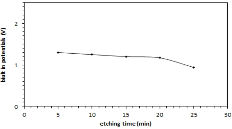
The built in potential of the porous silicon wafer was found as mentioned in the experimental work. Its value as shown in Figure 4,
exhibits decrease with increasing etching time and this result agrees with capacitance value result and this is due to the decrease of the junction depiletion layer
Figure (4): Curve show built-in potentials for PS/c-Si junction at different etching times
Conclusion
The electrical properties of show the dark current the decrease of current density with increasing etching time from 22 mA/ cmP
2
P
up to 4.3
mA/cmP 2
P
in the forward biasing while the ideality factor exhibits high value reaching up to 7.03 . The capacitance value also shows an increase with increasing etching time while the built in potentials decrease from 1.3 – 0.94 V
Reference
1. Ersin Kayahan a, Nazan Ceylan, , Applied Surface Science, Vol. 255, P.P. 2808–2812, (2008).
2. L.T. Canham, Appl. Phys. Lett. Vol. 57, issue 1046. (1990)
3. M.G. Berger, M. Tho¨ nissen, R. Arens-Fischer, H. Mu¨ nder, H. Lu¨ th, M. Arntzen, W.Theib, Thin Solid Films Vol. 225, issue 313, (1995)
4. P.G. Han, H. Wong, M.C. Poon, Colloid Surf. A Vol. 179 ,issue 171.(2001)
5. Y.W. Lu, X.W. Du, J. Sun, X. Han, J. Appl. Phys. Vol. 100, issue 063512, (2006)
6. C. L´evy-Cl´ement, S. Lust, M. Mamor, Physica Status Solidi (A), Vol. 202, no. 8, pp. 1390–1395, (2005).
7. Kasra behzad,wanmahmoodmat yunus, advances in optical technologies, vol. 2012, article id 581743, 9 pages, (2011).
8. Zhao yue, li dong-sheng, journal of zhejiang university science, vol. 6b, issue 11, p.p. 1135-1140, (2005).
9. Shinji yae," structural change in porous si by photoillumination
during metal particle enhanced etching", research, department of materials science and chemistry, graduate school of engineering, university of hyogo
10. Alwan m.alwan and narges z.abd alzahra, the influence of heating treatment on physical properties of porous silicon" journal of al-nahrain university, vol.12, No 2, P.P.76-81, (2009).
11. H H Afify, S H EL-Hefnawi, A Y Eliwa" Realization and Characterization of ZnO/n-Si Solar Cells by Spray Pyrolysis", Egypt. J. Solids, Vol. 28, No. 2, P.P. 243-254, (2005)
12. Saleem A Hussain, Matti N Makadsi, Khalid T Al-Rasoul, Naif
H.Al-Hardan" Current-Voltage studies on vacuum evaporated Al/CdTe/Al and Al/ZnTe/Al thin films systems" Baghdad University-College of Science-Physics department, Ministry of Science and technology-Directorate of Material Science.
13.W.L. Warren, K. Vandheusden, J.R. Scwank, D.M. Fleetwood,
P.S.Winokur, R.A.B. Devine, Appl. Phys. Lett. Vol. 68, No. 2993, (1996).
14.W. Hyoung Lee, Choochon Lee and J. Jang, Journal of Nano- Crystalline Solids,Vol.198, No.911, (1996)
15.A. Stesmans, V.V. Afanas’ev, Phys. Rev. B Vol. 54, No. R11129, (1996).
16. Alwan Mohamed Alwan, Mehdi Qasim Zayer, A thesis, Submitted to the Department of Applied Sciences, chapter 4 , 2010
17.D.Timokhov, F.Timokhov, Journal of Physical Studies,Vol.8, No. 2, P.P.173-177, (2004).