DESIGN OF HIGH-SPEED LOW-POWER
PULSE-TRIGGERED FLIP-FLOP USING TSMC-CMOS
TECHNOLOGY
I Anusha
1, A Madhavi
21
PG Student, Department of ECE, SVEB Engineering College/JNTUK, (India)
2
Assistant Professor, Department of ECE, SVEB Engineering College/JNTUK, (India)
ABSTRACT
Practically, clocking system like flip-flop (FF) consumes large portion of total chip power as high as 50%. In this brief, a novel low-power pulse-triggered flip-flop (P-FF) design is presented. Here an explicit type pulse-triggered structure and a modified true single phase clock latch based on a signal feed-through scheme is used. Pulse-triggered FF (P-FF) is a single-latch structure which is more popular than the conventional transmission gate (TG) and master-slave based FFs in high-speed applications by solving the long discharging path problem in conventional explicit type pulse-triggered FF(P-FF). All low power flip flops (FF) proposed are supplied with a supply voltage( VDD) ranging from 0.6v to 1.2v. Based on post-layout simulation results using TSMC CMOS 90-nm technology, the proposed design outperforms the conventional P-FF design. This paper concludes with the future challenges that must be met to design low power, high performance systems.
Keywords: Flip-Flop (FF), Pulse Triggered, TSMC CMOS
I. INTRODUCTION
Flip-flops (FFs) are the basic storage elements used extensively in all kinds of digital designs. In particular, digital designs nowadays often adopt intensive pipelining techniques and employ many FF-rich modules such as register file, shift register, and first in first out. It is also estimated that the power consumption of the clock system, which consists of clock distribution networks and storage elements, is as high as 50% of the total system power.
Pulse-triggered FF (P-FF), because of its single-latch structure, is more popular than the conventional transmission gate (TG) and master–slave based FFs in high-speed applications. Besides the speed advantage, its circuit simplicity lowers the power consumption of the clock tree system. A P-FF consists of a pulse generator for strobe signals and a latch for data storage. If the triggering pulses are sufficiently narrow, the latch acts like an edge-triggered FF. Since only one latch, as opposed to two in the conventional master–slave configuration, is needed, a P-FF is simpler in circuit complexity.
“1” and “0,” the design manages to shorten the longer delay by feeding the input signal directly to an internal node
of the latch design to speed up the data transition. This mechanism is implemented by introducing a simple pass transistor for extra signal driving. When combined with the pulse generation circuitry, it forms a new P-FF design with enhanced speed and power-delay-product (PDP) performances.
II. CONVENTIONAL TYPE P-FF DESIGNS
2.1. Conventional Explicit Type P-FF Design
PF-FFs, in terms of pulse generation, can be classified as an implicit or an explicit type. In an implicit type P-FF, the pulse generator is part of the latch design and no explicit pulse signals are generated. In an explicit type P-FF, the pulse generator and the latch are separate [7]. Without generating pulse signals explicitly, implicit type P-FFs is in general more power-economical. However, they suffer from a longer discharging path, which leads to inferior timing characteristics. Explicit pulse generation, on the contrary, incurs more power consumption but the logic separation from the latch design gives the FF design a unique speed advantage.
Its power consumption and the circuit complexity can be effectively reduced if one pulse generator is shares a group of FFs (e.g., an n-bit register). In this brief, we will thus focus on the explicit type P-FF designs only. To provide a comparison, some existing P-FF designs are reviewed first. Fig. 1 shows a classic explicit P-FF design, named data-close to- output (ep-DCO) [7]. It contains a NAND-logic-based pulse generator and a semi dynamic true-single-phase-clock (TSPC) structured latch design. In this P-FF design, inverters I3 and I4 are used to latch data, and inverters I1 and I2 are used to hold the internal node X.
The pulse width is determined by the delay of three inverters. This design suffers from a serious drawback, i.e., the internal node X is discharged on every rising edge of the clock in spite of the presence of a static input “1.” This
gives rise to large switching power dissipation. To overcome this problem, many remedial measures such as conditional capture, conditional recharge, conditional discharge, and conditional pulse enhancement scheme have been proposed.
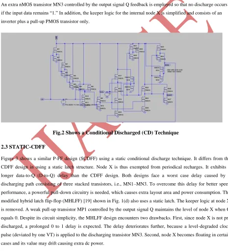
2.2 CDFF
An extra nMOS transistor MN3 controlled by the output signal Q feedback is employed so that no discharge occurs if the input data remains “1.” In addition, the keeper logic for the internal node X is simplified and consists of an
inverter plus a pull-up PMOS transistor only.
Fig.2 Shows a Conditional Discharged (CD) Technique
2.3 STATIC-CDFF
Fig.3 Static Conditional Discharge Technique
2.4 MHLFF
Fig.4 Modified Hybrid Latch Flip Flop
The modified hybrid latch flip-flop (MHLFF) [19] shown in Fig. 4 also uses a static latch. The keeper logic at node X is removed. A weak pull-up transistor MP1 controlled by the output signal Q maintains the level of node X when Q equals 0. Despite its circuit simplicity, the MHLFF design encounters two drawbacks. First, since node X is not pre discharged, a prolonged 0 to 1 delay is expected. The delay deteriorates further, because a Level-degraded clock pulse (deviated by one VT) is applied to the discharging transistor MN3. Second, node X becomes floating in certain
III.PROPOSED P-FF DESIGN
Recalling the four circuits reviewed in Section II, they all encounter the same worst case timing occurring at 0 to 1 data transitions. Referring to Fig. 5, the proposed design adopts a signal feed-through technique to improve this delay. Similar to the SCDFF design, the proposed design also employs a static latch structure and a conditional discharge scheme to avoid superfluous switching at an internal node. However, there are three major differences that lead to a unique TSPC latch structure and make the proposed design distinct from the previous one. First, a weak pull-up pMOS transistor MP1with gate connected to the ground is used in the first stage of the TSPC latch. This gives rise to a pseudo-nMOS logic style design ,and the charge keeper circuit for the internal node X can be saved .In addition to the circuit simplicity, this approach also reduces the load capacitance of node X [20], [21].Second, a pass transistor MNx controlled by the pulse clock is included so that input data can drive node Q of the latch directly (the signal feed-through scheme).Along with the pull-up transistor MP2 at the second stage inverter of the TSPC latch, this extra passage facilitates auxiliary signal driving from the input source to node Q. The node level can thus be quickly pulled up to shorten the data transition delay. Third, the pull-down network of the second stage inverter is completely removed. Instead, the newly employed pass transistor MNx provides a discharging path. The role played by MNx is thus twofold, i.e., providing extra driving to node Q during 0 to 1 data transitions, and discharging node Q during “1” to “0” data transitions. Compared with the latch structure used in SCDFF design, the circuit savings of
the proposed design include a charge keeper , a pull-down network and a control inverter .The only extra component introduced is an nMOS pass transistor to support signal feedthrough.
IV. COMPARISON OF VARIOUS FF DESIGNS
Performance of FF Designs design does not use the least number of transistors; it has the smallest layout area. This is mainly attributed to the signal feed-through scheme, which largely reduces the transistor sizes on the discharging path. In terms of power behavior, the proposed design is the most efficient in five out of the six test patterns. The savings vary in different combinations of test pattern and FF design. For example, if a 25% data switching test pattern is used, the proposed design is more power economical than all except the ACFF design. Its power saving against ep-DCO, CDFF, SCDFF and MHLFF are 22.7%, 6.9%, 8.1% and 8.3% respectively [16]. The ep-DCO design consumes the largest power because of the superfluous internal node discharging problem. ACFF design [2] power efficiency is even more significant in the cases of zero or low input data switching activity.
Similarly, another non-P-FF design, the TGFF, performs lightly better than the proposed one in the case of static input patterns (0% switching activity). However, when a test pattern with 100%switching activity is applied, the proposed deign is 9% and 12%more power efficient than the ACFF design and the TGFF design, respectively. This can be explained by the power overhead of the pulse generator regardless of the data patterns in all P-FF designs. The significance of this overhead, however, decreases as the data switching activity increases. The leakage powers of all FF designs under different combinations of clock and input signals. A possible concern on the proposed design arises from the pseudo-nMOS logic in the first stage. Although an always-on MP1 prevents node X from full voltage swing, it does not result in any dc power consumption problem. Since the proposed signal feed-through scheme requires occasional signal driving from the input node directly to the output node, we also calculate the power drawn by the pass transistor MNx (the extra power consumption caused by the signal feed through scheme).Post-layout simulation results show that this part accounts for only8.47% of the total power consumption when the input data switching activity is 100%. The percentage reduces to 1.62% when the input data switching activity is lowered to 12.5%.Finally the lay out decreased with 24 number of transistors.
Feature Comparison of Various FF Designs:
FF designs DCOep - CDFF SCDFF MHLFF PROPOSED
Numbers of transistors 28 30 31 19 24
Lay out area (µm²) 76.99 89.70 88.99 77.97 69.01
Setup time (ps) -84.56 -88.91 -44.67 1.49 -84.76
Hold time (ps) 110 123.4 122.9 93.5 119.9
Minimum D to Q Delay(ps)
117.9 129.6 140.0 172.9 108.9
Average Power (100% Activity)µW
34.01 34.07 35.04 31.07 30.99
Supply voltage (VDD)v 0.8 0.8 0.8 0.8 0.6
V. SIMULATION RESULTS
1] is used for all P-FF designs except the MHLFF design, which employs its own pulse generation circuitry as specified in Fig.4.The target technology is the TSMC 90-nm CMOS process. Since pulse width design is crucial to the correctness of data capture as well as the power consumption [10]–[13], the transistors of the pulse generator logic are sized for a design spec of 120 ps in pulse width in the TT case. The sizing also ensures that the pulse generators can function properly in all process corners. With regard to the latch structures, each P-FF design is individually optimized subject to the product of power and D-to-Q delay. To mimic the signal rise and fall time delays, input signals are generated through buffers. Since the proposed design requires direct output driving from the input source, for fair comparisons the power consumption of the data input buffer (an inverter) is included. The output of the FF is loaded with a20-pf capacitor. An extra loading capacitance of 3 pf is also placed at the output of the clock buffer [18]. The operating condition used in simulations is 50 MHz/0.6v to 50MHz/1.2v
Fig: 5 Monte Carlo Simulation Results
Fig: 7 CDFF Simulations Results
Fig: 8 Static-CDFF Simulation Results
Fig : 10 Proposed PFF Design Simulation Results
VI. CONCLUSION
In this brief, we presented a novel P-FF design by employing a modified TSPC latch structure incorporating a mixed design style consisting of pass transistor and pseudo-nMOS logic. The key idea was to provide a signal feed through from input source to the internal node of the latch, which would facilitate extra driving to shorten the transition time and enhance both power and speed performance. Supply voltage is mainly dependent on low power dissipation in future p-FF design by employing a modified latch structure. The design was intelligently achieved by employing a simple pass transistor. Extensive simulations were
conducted, and the results did support the claims of the proposed design in various performance aspects.
REFERENCES
[1] H. Kawaguchi and T. Sakurai, “A reduced clock-swing flip-flop (RCSFF)for 63% power reduction,” IEEE J.
Solid-State Circuits, vol. 33, no. 5,pp. 807–811, May 1998.
[2] K. Chen, “A 77% energy saving 22-transistor single phase clocking D flip-flop with adoptive-coupling configuration in 40 nm CMOS,” in Proc.IEEE Int. Solid-State Circuits Conf., Nov. 2011, pp. 338–339.
[3] E. Consoli, M. Alioto, G. Palumbo, and J. Rabaey, “Conditional pushpullpulsed latch with 726 fJops energy delay product in 65 nm CMOS,”in Proc. IEEE Int. Solid-State Circuits Conf., Feb. 2012, pp. 482–483.
[4] H. Partovi, R. Burd, U. Salim, F.Weber, L. DiGregorio, and D.Draper, “Flow-through latch and edge-triggered flip-flop hybrid elements,”in Proc. IEEE Int. Solid-State Circuits Conf., Feb. 1996,pp. 138–139.
[5] F. Klass, C. Amir, A. Das, K. Aingaran, C. Truong, R. Wang, A. Mehta,R. Heald, and G. Yee, “A new family of semi-dynamic and dynamicflip-flops with embedded logic for high-performance processors,” IEEEJ. Solid-State Circuits, vol. 34, no. 5, pp. 712–716, May 1999.
[6] V. Stojanovic and V. Oklobdzija, “Comparative analysis of masterslave latches and flip-flops for
[7] J. Tschanz, S. Narendra, Z. Chen, S. Borkar, M. Sachdev, and V. De,“Comparative delay and energy of single
edge-triggered and dual edgetriggered pulsed flip-flops for high-performance microprocessors,” inProc. ISPLED, 2001, pp. 207–212.
[8] S. D. Naffziger, G. Colon-Bonet, T. Fischer, R. Riedlinger, T. J.Sullivan, and T. Grutkowski, “The implementation of the Itanium2 microprocessor,” IEEE J. Solid-State Circuits, vol. 37, no. 11,pp. 1448–1460, Nov. 2002.
[9] S. Sadrossadat, H. Mostafa, and M. Anis, “Statistical design frameworkof sub-micron flip-flop circuits
considering die-to-die and within-dievariations,” IEEE Trans. Semicond. Manuf., vol. 24, no. 2, pp. 69–79,Feb. 2011.
[10] M. Alioto, E. Consoli, and G. Palumbo, “General strategies to designnanometer flip-flops in the energy-delay space,” IEEE Trans. CircuitsSyst., vol. 57, no. 7, pp. 1583–1596, Jul. 2010.
[11] M. Alioto, E. Consoli, and G. Palumbo, “Flip-flop energy/performanceversus Clock Slope and impact on the clock network design,” IEEETrans. Circuits Syst., vol. 57, no. 6, pp. 1273–1286, Jun. 2010.
[12] M. Alioto, E. Consoli, and G. Palumbo, “Analysis and comparison inthe energy-delay-area domain of nanometer CMOS flip-flops: Part I- methodology and design strategies,” IEEE Trans. Very Large ScaleIntegr. (VLSI) Syst., vol. 19, no. 5, pp. 725–736, May 2011.
[13] M. Alioto, E. Consoli and G. Palumbo, “Analysis and comparison inthe energy-delay-area domain of nanometer CMOS flip-flops: Part II -results and figures of merit,” IEEE Trans. Very Large Scale Integr. (VLSI)Syst., vol. 19, no. 5, pp. 737–750, May 2011.
[14] B. Kong, S. Kim, and Y. Jun, “Conditional-capture flip-flop for statisticalpower reduction,” IEEE J. Solid-State Circuits, vol. 36, no. 8,pp. 1263–1271, Aug. 2001.
[15] N. Nedovic, M. Aleksic, and V. G. Oklobdzija, “Conditional prechargetechniques for power-efficient dual-edge clocking,” in Proc. Int. Symp.Low-Power Electron. Design, Aug. 2002, pp. 56–59.
[16] P. Zhao, T. Darwish, and M. Bayoumi, “High-performance and low power conditional discharge flip-flop,” IEEE Trans. Very Large Scale Integr. (VLSI) Syst., vol. 12, no. 5, pp. 477–484,May 2004.
[17] M.-W. Phyu, W.-L. Goh, and K.-S. Yeo, “A low-power staticdual edge triggered flip-flop using an output-controlled discharge configuration,”in Proc. IEEE Int. Symp. Circuits Syst., May 2005,pp. 2429–2432.
[18] Y.-T. Hwang, J.-F. Lin, and M.-H. Sheu, “Low power pulsetriggeredflip-flop design with conditional pulse enhancement scheme,”IEEE Trans. Very Large Scale Integr. (VLSI) Syst., vol. 20, no. 2,pp. 361–366, Feb.
2012.
[19] S. H. Rasouli, A. Khademzadeh, A. Afzali-Kusha, and M. Nourani,“Low power single- and double-edge-triggered flip-flops for highspeed applications,” IEE Proc. Circuits Devices Syst., vol. 152, no. 2,pp. 118–122, Apr. 2005.
[20] H. Mahmoodi, V. Tirumalashetty, M. Cooke, and K. Roy, “Ultra lowpower clocking scheme using energy recovery and clock gating,” IEEETrans. Very Large Scale Integr. (VLSI) Syst., vol. 17, no. 1, pp. 33–44,Jan.
[21] P. Zhao, J. McNeely, S. Venigalla, G. P. Kumar, M. Bayoumi, N. Wang,and L. Downey,
“Clocked-pseudo-NMOS flip-flops for level conversionin dual supply systems,” IEEE Trans. Very Large Scale Integr. (VLSI)Syst., vol. 17, no. 9, pp. 1196–1202, Sep. 2009.
[22] V. G. Oklobdzija, “Clocking and clocked storage elements in a multigigahertz environment,” IBM J. Res.
Devel., vol. 47, no. 5, pp. 567–584,Sep. 2003