Open Access Dissertations Theses and Dissertations
Fall 2014
Computing with Spintronics: Circuits and
architectures
Rangharajan Venkatesan
Purdue University
Follow this and additional works at:https://docs.lib.purdue.edu/open_access_dissertations Part of theElectrical and Electronics Commons
This document has been made available through Purdue e-Pubs, a service of the Purdue University Libraries. Please contact [email protected] for additional information.
Recommended Citation
Venkatesan, Rangharajan, "Computing with Spintronics: Circuits and architectures" (2014).Open Access Dissertations. 377.
GRADUATE SCHOOL
Thesis/Dissertation Acceptance
This is to certify that the thesis/dissertation prepared By
Entitled
For the degree of
Is approved by the final examining committee:
Chair
To the best of my knowledge and as understood by the student in the Research Integrity and
Copyright Disclaimer (Graduate School Form 20), this thesis/dissertation adheres to the provisions of
Purdue University’s “Policy on Integrity in Research” and the use of copyrighted material.
Approved by Major Professor(s): ____________________________________ ____________________________________
Approved by:
Head of the Graduate Program Date
Rangharajan Venkatesan
Computing with Spintronics: Circuits and Architectures
Doctor of Philosophy ANAND RAGHUNATHAN ARIJIT RAYCHOWDHURY BYUNGHOO JUNG KAUSHIK ROY ANAND RAGHUNATHAN M. R. Melloch 10-01-2014
A Dissertation Submitted to the Faculty
of
Purdue University by
Rangharajan Venkatesan
In Partial Fulfillment of the Requirements for the Degree
of
Doctor of Philosophy
December 2014
Purdue University West Lafayette, Indiana
ACKNOWLEDGMENTS
First and foremost, I would like to express my sincere gratitude to my advisor, Prof. Anand Raghunathan for his outstanding support throughout my Ph.D. His excellent guidance enabled me to explore several different research topics of my Ph.D. with relative ease. His constant motivation and encouragement played a significant role in overcoming various hurdles and was a great inspiration towards achieving different milestones during my Ph.D. I would also like to thank him for creating a diverse learning atmosphere in the lab, which enabled me to acquire knowledge across a wide spectrum in both technical and non-technical areas.
I would like to thank Prof. Kaushik Roy for his support and mentorship. His advice and motivation was a great encouragement for me towards pursuing exciting ideas during my Ph.D. I would like to thank Prof. Byunghoo Jung and Prof. Arijit Raychowdhury for serving in my doctoral committee and for providing insightful thoughts and feedback during my Ph.D.
My sincere thanks to the alumni and current members of Integrated Systems Lab-oratory (ISL) and Nanoelectronics Research LabLab-oratory (NRL) for their collaboration and friendship during my Ph.D. Special thanks to my parents, Venkatesan and Jailak-shmi, and my sister Sundharavalli for their support, love and affection throughout my entire life.
TABLE OF CONTENTS
Page
LIST OF TABLES . . . vii
LIST OF FIGURES . . . viii
ABSTRACT . . . xi
1 INTRODUCTION . . . 1
1.1 CMOS scaling challenges . . . 3
1.1.1 Process variations . . . 3
1.1.2 Power and Temperature . . . 4
1.1.3 Reliability . . . 5
1.2 Spintronics. . . 6
1.2.1 Spintronic Memory . . . 7
1.2.2 Spintronic Logic. . . 9
1.2.3 Motivation for new circuits and architectures. . . 11
1.3 Thesis overview . . . 15
1.4 Thesis organization . . . 16
2 RELATED WORK . . . 20
2.1 Emerging memory technologies . . . 20
2.1.1 Device and circuit optimizations . . . 21
2.1.2 Architectural design and evaluation . . . 22
2.2 Emerging logic devices . . . 23
2.3 Thesis contributions . . . 25
3 BACKGROUND . . . 27
3.1 STT-MRAM. . . 27
3.2 Domain Wall Memory . . . 28
Page 4 DOMAIN-SPECIFIC MANY-CORE PROCESSOR FOR RECOGNITION
AND MINING . . . 33
4.1 Many-core RM processor design . . . 35
4.2 RM processor modeling . . . 40
4.3 Experimental results . . . 42
4.3.1 Experimental setup . . . 43
4.3.2 RM processor evaluation . . . 43
4.3.3 Analysis of benefits of DWM and STT-MRAM. . . 47
4.3.4 Circuit optimization: Voltage scaling . . . 48
4.3.5 Architectural exploration . . . 50
4.4 Conclusion . . . 54
5 TAPESTRI: DESIGN OF DWM TAPES WITH SHIFT-BASED WRITE 55 5.1 Shift-based write . . . 57
5.2 Tapestribit-cell designs . . . . 57
5.2.1 1bitDWM . . . 58
5.2.2 MultibitDWM . . . 59
5.2.3 Tapestri bit-cell characteristics . . . . 60
5.3 Cache characteristics . . . 64
5.3.1 Impact of bits/tape of multibitDWM . . . 66
5.4 Conclusion . . . 66
6 TAPECACHE: CACHE DESIGN BASED ON DWM TAPES . . . 68
6.1 Multi-port read-skewed multibitDWM bit-cell . . . 70
6.2 DWM cache architecture . . . 72
6.2.1 Hybrid L2 cache design . . . 74
6.2.2 Bit-interleaved DWM Block-Cluster organization . . . 76
6.2.3 Head management policies . . . 78
6.3 Experimental methodology . . . 83
Page 6.3.2 Experimental setup . . . 83 6.4 Experimental results . . . 84 6.4.1 Results summary . . . 85 6.4.2 Cache characteristics . . . 85 6.4.3 Architectural evaluation . . . 87
6.4.4 Design space exploration . . . 89
6.5 Conclusion . . . 91
7 STAG: SPINTRONIC-TAPE ARCHITECTURE FOR GPGPU CACHE HI-ERARCHIES . . . 92
7.1 STAG architecture . . . 94
7.1.1 L1 cache design with 1bitDWM . . . 96
7.1.2 Hybrid L2 cache design . . . 97
7.1.3 Shift aware promotion buffer . . . 103
7.2 Experimental methodology . . . 106
7.3 Experimental results . . . 108
7.3.1 Performance comparison . . . 108
7.3.2 Energy comparison . . . 110
7.3.3 Design space exploration . . . 111
7.4 Conclusion . . . 116
8 SPINTASTIC: SPIN-BASED STOCHASTIC LOGIC FOR ENERGY-EFFICIENT COMPUTING. . . 117
8.1 Background: Stochastic Computing . . . 120
8.2 Spintastic: Device fundamentals . . . . 122
8.3 Spintasticlogic design . . . . 122
8.3.1 Spintronic Stochastic Number Generator . . . 123
8.3.2 Spintronic Stochastic Bitstream Permuter . . . 126
8.3.3 Spintronic Stochastic-to-Binary Converter . . . 129
8.3.4 Spintronic Stochastic Arithmetic Units . . . 130
Page
8.5 Experimental methodology . . . 132
8.6 Experimental results . . . 134
8.6.1 Energy benefits and analysis . . . 134
8.6.2 Sensitivity to bitstream length . . . 136
8.6.3 Application-level analysis. . . 137
8.7 Conclusion . . . 138
9 DEVICE TO ARCHITECTURE SIMULATION FRAMEWORK . . . . 139
9.1 Spin device simulator . . . 140
9.1.1 STT-MRAM . . . 140 9.1.2 DWM . . . 140 9.2 Spin-CACTI . . . 141 9.2.1 Area . . . 141 9.2.2 Dynamic energy . . . 144 9.2.3 Leakage power. . . 145 9.2.4 Access latency . . . 145 10 CONCLUSIONS . . . 147 REFERENCES . . . 149 VITA . . . 161
LIST OF TABLES
Table Page
4.1 Second level memory access characteristics for SVM and k-means . . . 36
4.2 RM processor configuration . . . 43
4.3 Comparison of the spin-based design of the RM processor with the baseline implementation . . . 44
6.1 System configuration . . . 84
7.1 GPGPU configuration . . . 106
7.2 GPGPU workloads . . . 106
LIST OF FIGURES
Figure Page
1.1 Evolution of electronic industry . . . 2
1.2 Variation in ION and IOF F of transistors at 65nm node . . . 3
1.3 Power and performance trend in Intel microprocessors. . . 4
1.4 Lifetime degradation with CMOS scaling . . . 6
1.5 Spin-Transfer Torque Magnetic RAM . . . 7
1.6 Domain Wall Memory . . . 8
1.7 Nano-Magnetic Logic . . . 10
1.8 All-Spin Logic . . . 11
1.9 Comparison of different memory technologies. . . 11
1.10 Comparison of area and power consumption of ASL with CMOS for Leon-Sparc processor . . . 12
1.11 Growth in number of processing elements or cores in CPUs and GPUs 13 1.12 Growth in on-chip memory of CPUs and GPUs . . . 14
1.13 Thesis overview . . . 15
3.1 STT-MRAM bit-cell . . . 27
3.2 DWM macro-cell . . . 29
3.3 ASL inverter . . . 31
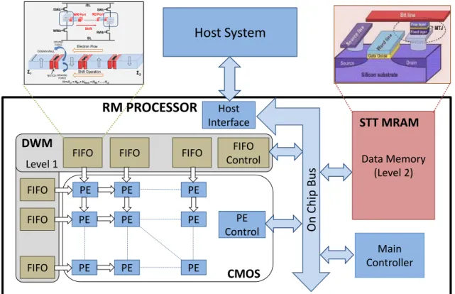
4.1 Many-core RM processor design . . . 35
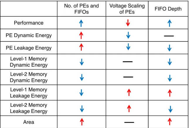
4.2 Impact of tuning architectural parameters on the RM processor charac-teristics . . . 38
4.3 RM processor modeling framework . . . 40
4.4 Spin-based RM processor: Design strategies . . . 44
4.5 Energy, Performance, and Energy-Delay Product comparison to analyze the benefits of DWM and STT-MRAM . . . 45
Figure Page
4.7 Effect of voltage scaling for k-means algorithm . . . 49
4.8 Effect of FIFO size on energy consumption for SVM algorithm . . . 52
4.9 Effect of increasing the no. of PEs on energy and performance for SVM algorithm . . . 53
5.1 Different write mechanisms in spintronic memories . . . 57
5.2 Schematic of Tapestri bit-cells . . . . 58
5.3 Comparison of write characteristics of shift-based write with MTJ-based write . . . 61
5.4 Layout of STT-MRAM, 1bitDWM, and MultibitDWM bit-cells . . . . 62
5.5 Read/write stability of Tapestribit-cells . . . . 64
5.6 Comparison of DWM characteristics with SRAM and STT-MRAM . . 64
5.7 Impact of increasing bits/tape on cache area and access latency . . . . 66
6.1 Logical view of a multi-port read-skewed multibitDWM bit-cell . . . . 70
6.2 TapeCache organization . . . 72
6.3 Hybrid L2 cache migration policy . . . 75
6.4 Bit-interleaved data array organization . . . 77
6.5 Comparison of different cache management policies . . . 80
6.6 Adaptive preshifting policy. . . 82
6.7 Comparison of area, energy and performance across different memory tech-nologies . . . 85
6.8 Comparison of L1 and L2 cache characteristics . . . 86
6.9 Comparison of energy consumption of cache across different memory tech-nologies . . . 88
6.10 Performance comparison between different memory technologies . . . . 89
6.11 Design space exploration for TapeCache . . . 90
7.1 STAG architecture overview . . . 95
7.2 Bit-interleaved DWM tape cluster organization . . . 98
7.3 Preshifted head policy . . . 100
Figure Page
7.5 Access pattern of neural network benchmark . . . 103
7.6 SaPB operation . . . 104
7.7 Performance of different cache designs under iso-area conditions . . . . 109
7.8 Energy consumption of different cache designs under iso-area conditions 110 7.9 Impact of bits/tape on performance under iso-area conditions . . . 112
7.10 Energy consumption for various bits/tape configurations . . . 113
7.11 Impact of bits/tape on EDP . . . 114
7.12 Impact of cache management policies on performance (Normalized to re-stored head policy) . . . 115
7.13 Impact of L2 cache size for different bits per tape . . . 116
8.1 Structure of a stochastic computing circuit . . . 120
8.2 Spintronic Random Number Generator (Spin-RNG) . . . 123
8.3 Spintronic Stochastic Number Generator (Spin-SNG) . . . 124
8.4 Spintronic Stochastic Bitstream Permuter . . . 126
8.5 Logical view of Spintronic Stochastic Bitstream Permuter . . . 128
8.6 Spintronic Stochastic-to-Binary Converter (Spin-SBC) . . . 130
8.7 Stochastic multiplier design . . . 131
8.8 Comparison of energy consumption of Spintastic with CMOS baseline designs . . . 134
8.9 Energy breakdown for 1D-DCT . . . 135
8.10 Impact of bitstream length on the energy consumption . . . 136
8.11 Application-level energy comparison . . . 138
9.1 Device to architecture simulation framework . . . 139
ABSTRACT
Venkatesan, Rangharajan Ph.D., Purdue University, December 2014. Computing with Spintronics: Circuits and Architectures. Major Professor: Prof. Anand Raghu-nathan.
With the scaling of semiconductor technology approaching its fundamental limits, several potential replacements are being actively explored to the mainstays of Silicon and CMOS. Among them, spintronics, which uses electron ‘spin’ as the state variable to represent and process information, has attracted significant interest in recent years. Spintronic devices are considered promising due to their non-volatility, near-zero leakage, and high integration density, all of which compare favorably to CMOS. How-ever, they are not superior in all respects. Spintronic memories such as Spin-Transfer Torque Magnetic RAM (STT-MRAM) require high write energy and latency. Spin-tronic logic proposals such as All-Spin Logic (ASL) are limited by large current re-quirement for high speed operation, high short circuit power and low spin-diffusion length of spin interconnects. Therefore, spintronic devices are neither universal nor drop-in replacements. This creates the need for new designs at the circuit and archi-tecture levels that exploit the strengths of spintronic devices and mask their weak-nesses.
This thesis makes the following contributions towards the design of computing platforms with spintronic devices.
• It explores the use of spintronic memories in the design of a domain-specific
pro-cessor for an emerging class of data-intensive applications, namely recognition, mining and synthesis (RMS). Two different spintronic memory technologies— Domain Wall Memory (DWM) and STT-MRAM—are utilized to realize the different levels in the memory hierarchy of the domain-specific processor, based
on their respective access characteristics. Architectural tradeoffs created by the use of spintronic memories are analyzed. The proposed design achieves 1.5X-4X improvements in energy-delay product compared to a CMOS baseline.
• It describes the first attempt to use DWM in the cache hierarchy of
general-purpose processors. DWM promises unparalleled density by packing several bits of data into each bit-cell. TapeCache, the proposed DWM-based cache archi-tecture, utilizes suitable circuit and architectural optimizations to address two key challenges (i) the high energy and latency requirement of write operations and (ii) the need for shift operations to access the data stored in each DWM bit-cell. At the circuit level, DWM bit-cells that are tailored to the distinct de-sign requirements of different levels in the cache hierarchy are proposed. At the architecture level, TapeCache proposes suitable cache organization and manage-ment policies to alleviate the performance impact of shift operations required to access data stored in DWM bit-cells. TapeCache achieves more than 7X im-provements in both cache area and energy with virtually identical performance compared to an SRAM-based cache hierarchy.
• It investigates the design of the on-chip memory hierarchy of general-purpose
graphics processing units (GPGPUs)—massively parallel processors that are optimized for data-intensive high-throughput workloads—using DWM. STAG, a high density, energy-efficient Spintronic-Tape Architecture for GPGPU cache hierarchies is described. STAG utilizes different DWM bit-cells to realize differ-ent memory arrays in the GPGPU cache hierarchy. To address the challenge of high access latencies due to shifts, STAG predicts upcoming cache accesses by leveraging unique characteristics of GPGPU architectures and workloads, and prefetches data that are both likely to be accessed and require large numbers of shift operations. STAG achieves 3.3X energy reduction and 12.1% performance improvement over CMOS SRAM under iso-area conditions.
• While the potential of spintronic devices for memories is widely recognized, their
utility in realizing logic is much less clear. The thesis presents Spintastic,
a new paradigm that utilizes Stochastic Computing (SC) to realize spintronic logic. In SC, data is encoded in the form of pseudo-random bitstreams, such that the probability of a ‘1’ in a bitstream corresponds to the numerical value that it represents. SC can enable compact, low-complexity logic implementations
of various arithmetic functions. Spintastic establishes the synergy between
stochastic computing and spin-based logic by demonstrating that they mutually alleviate each other’s limitations. On the one hand, various building blocks of SC, which incur significant overheads in CMOS implementations, can be efficiently realized by exploiting the physical characteristics of spin devices. On the other hand, the reduced logic complexity and low logic depth of SC circuits alleviates the shortcomings of spintronic logic. Based on this insight, the design of spin-based stochastic arithmetic circuits, bitstream generators, bitstream permuters and stochastic-to-binary converter circuits are presented.
Spintastic achieves 7.1X energy reduction over CMOS implementations for
a wide range of benchmarks from the image processing, signal processing, and RMS application domains.
• In order to evaluate the proposed spintronic designs, the thesis describes various
device-to-architecture modeling frameworks. Starting with devices models that are calibrated to measurements, the characteristics of spintronic devices are successively abstracted into circuit-level and architectural models, which are incorporated into suitable simulation frameworks.
The results presented in this thesis suggest that spintronics can add significant value to the design of future computing platforms. Spintronic devices are well-suited for designing memories, but suitable circuits and architectures (as proposed in this the-sis) can significantly enhance their benefits. On the other hand, although spintronic logic faces fundamental challenges as a drop-in replacement for CMOS, efficient
im-plementations may be possible for some application domains whose computational characteristics match those of spintronic devices.
1. INTRODUCTION
In the history of the semiconductor industry, an endeavor to deliver compact, high performance systems at low power has been the major driving force. Figure 1.1 shows a timeline of some of the important advances in the device technology during the evolution of the semiconductor industry. Historically, technology scaling, which involved shrinking of device dimensions and voltage scaling simultaneously, was the major source of the key benefits in terms of density, power and performance. However, the industry has seen multiple tipping points when a fundamental change in the device technology was required to achieve sustained benefits. These include the transition from vacuum tubes to Bipolar Junction Transistors (BJTs) in the late 1940s and the adoption of Complementary Metal Oxide Semiconductor (CMOS) technology in the 1980s. As CMOS technology scales deep into the nanometer regime, further scaling is
facing a number of challenges due to increased variations, higher leakage power, etc.
and many researchers believe that the integrated circuit industry is nearing another such tipping point. This has led to an intense quest for identifying the “next switch”,
and several new devices (e.g. III-V tunnel FET (TFET) [1], nano-electro-mechanical
switches (NEMS) [2], carbon nanotube (CNT) [3], graphene nanowire [4], spintronic
devices [5–7], etc.) have been proposed as potential CMOS replacements.
A promising direction that has emerged from this quest isspintronics, which uses
spin rather than charge as the state variable to represent and process information. Spintronic devices are considered highly promising due to their non-volatility (they can retain data even when the power supply is switched off leading to very low leakage power), and high integration density resulting in smaller area footprint compared to CMOS. Spin-based devices such as Spin-Transfer Torque Magnetic RAM
(STT-MRAM) [10–13], domain wall memory (DWM) [14–17] etc. are widely considered
1900 10 20 30 40 50 60 70 80 90 2000 2010 2020 Diode Triode MOSFET MISFET BJT – 1st Transistor Si-MOSFET First Microprocessor - 4004, 10um PMOS technology
First CMOS Microprocessor - 80286, 1.5um CMOS technology
Intel’s dual-core processor - Montecito,
90nm CMOS technology
First FinFET based processor – Ivy Bridge, 22nm FinFET technology
1
stElectronic Circuits
Solid-state Circuits
Silicon Technology
CMOS Technology
FinFET Technology
Low Power High Speed High Integration Low Power High Speed High Integration High Integration Low power Transistor Concept TFET ?? CNT Nanowire NEMS SpintronicsFig. 1.1.: Evolution of semiconductor industry [8, 9]
prototypes and early commercial products have underscored the promise of spin-based memories [18–22]. Recent research efforts have shown the feasibility of realizing logic functionality (both Boolean and non-Boolean) using spin-based devices [23–29]. While spintronic devices are highly promising, a comprehensive circuit-to-architecture study is required to explore the design of future spin-based computing platforms. This thesis attempts to perform such a study.
In the following sections, we first present an overview of current CMOS scaling challenges. We then describe some of the promising spintronic device technologies and motivate the need for new circuits and architectures from both the device as well as application perspective. Finally, we conclude this chapter with a brief description of the contributions of this thesis and an overview of the remaining chapters.
1.1 CMOS scaling challenges
Scaling of CMOS technology, in accordance with Moore’s law, has provided with recurring benefits in terms of increased processing capabilities, higher performance and lower energy consumption. However, continued scaling into the nanometer regime has thrown up a number of challenges such as increased process variations, higher
leakage power, decrease in reliability of devices, etc. Let us examine these issues in
more detail. 1.1.1 Process variations
N
o
rm
a
li
z
e
d
I
O NFig. 1.2.: Variation in ION and IOF F of transistors at the 65nm node [30]
The inability of the lithographic process to precisely control the process parame-ters has resulted in process variations becoming a major challenge to the continued scaling of CMOS technology [31, 32]. Variations in parameters like channel length,
thickness of gate oxide, dopant concentration, etc. cause corresponding changes in
the transistor’s electrical characteristics like threshold voltage, eventually resulting in variations in the transistor switching characteristics. Figure 1.2 illustrates the im-pact of process variations on the ON and OFF currents of the transistors at the 65nm
node. We can see that the leakage current varies by about two orders of magnitude, while ON current varies by a factor of two.
Increased variations force the designers to introduce design guard bands in order to ensure correct functionality even under worst case conditions, thereby resulting in over-design of the systems. As device dimensions shrink further with scaling of technology, variations become more significant and require larger and larger guard bands. This could eventually negate all the benefits of scaling, thereby bringing about the end of CMOS technology scaling.
1.1.2 Power and Temperature
!"#$%&'()&*+$",-&
!!!"#$%&'&()#&!*+++,! !!!-.)/0!12334!*567,! !!!8)93#!*:,! !!!83#;<-.)/0!*=>8,!
Scaling of technology resulted in exponential increase in both the number of tran-sistors integrated per chip as well as the frequency of their operation. Figure 1.3 shows the trends in transistor count and frequency for Intel microprocessors. These have been the major contributors to the improvement in performance of the system till early 2000s. However, the increase in the transistor count and frequency also re-sulted in an increase in the power consumption of chips, as shown in Figure 1.3. With the total power consumption reaching the power budget of 100W, the scaling trend had already changed causing tectonic shifts (such as the switch to parallelism rather than clock frequency as the primary driver of performance in microprocessors) [34].
Another major challenge to the scaling of CMOS technology is the increase in power density and the corresponding increase in the on-chip temperature. Traditional scaling of CMOS technology involved scaling of threshold voltage and the supply volt-age along with transistor dimensions, resulting in power density remaining constant. However, with the increase in short channel effects and the corresponding increase in the leakage current, the threshold voltage cannot be scaled at the same rate as that of the transistor dimensions. This in turn has slowed down the rate of supply voltage scaling in order to maintain performance, resulting in an increase in the power density of the chip. Increase in power density causes the on-chip temperature to rise leading to thermal concerns.
1.1.3 Reliability
The reliability concerns of CMOS technology arise from a number of factors such as hot carrier injection (HCI), negative bias temperature instability (NBTI), time
dependent dielectric breakdown (TDDB), electromigration,etc. HCI occurs when an
high energy electron gets trapped in the gate oxide. NBTI is caused due to gen-eration of positive oxide charge and interface traps in PMOS under negative bias conditions [35]. HCI and NBTI causes the threshold voltage of transistors to in-crease, resulting in performance degradation. TDDB is a phenomenon that is caused
by the formation of conducting paths through the gate oxide due to electron tun-neling current. Unlike HCI or NBTI, which result in gradual degradation, TDDB is a catastrophic failure causing the circuit to malfunction. Electromigration is the transport of material caused by the gradual movement of the ions in a conductor, resulting in increases in the resistances of the interconnects.
Fig. 1.4.: Lifetime degradation with CMOS scaling [36]
With scaling of CMOS technology, the effect of NBTI, HCI, TDDB and electro-migration increases, resulting in considerable reliability degradation. This results in reduction in the lifetime with each technology generation, as shown in Figure 1.4.
As a result of the above mentioned challenges, the scaling of CMOS technology is likely to come to an end within the next decade. This has led to the search for alternate device technologies that can complement or potentially replace the existing CMOS technology. Spintronics is widely considered to be highly promising and we present a brief description of it next.
1.2 Spintronics
Spintronics is an emerging technology in which the processing, storage, and com-munication of data is performed by means of electron-spin along with or instead of electron-charge. The basic unit in a spintronic device is a magnet that can have two different magnetization directions representing 0 and 1. A number of different
spintronic devices have been proposed for realizing both memory and logic. In the following sections, we describe some of the promising spintronic memory and logic technologies.
1.2.1 Spintronic Memory
With the increase in contribution of on-chip memory to the total chip area and power consumption, there has been a surge in the number of research efforts to identify suitable replacements for CMOS-based memories (SRAM and DRAM). Sev-eral new memory technologies— Ferroelectric RAM (FeRAM), Phase Change RAM
(PCRAM), STT-MRAM, DWM, etc. have been proposed as potential replacements.
Among them, spintronic memory technologies (STT-MRAM and DWM) are consid-ered as potential candidates for future on-chip memory designs due to their high density, non-volatility leading to low leakage power and read access latencies that are comparable to SRAM/DRAM. In the following sections, we present a brief descrip-tion of the two promising spintronic memory technologies – STT-MRAM and DWM – and analyze their benefits and challenges.
Spin-Transfer Torque Magnetic RAM
Source Drain Silicon Substrate Free Layer Fixed Layer Gate Oxide Bitline MTJ
Spin-Transfer Torque Magnetic RAM or STT-MRAM is a spintronic memory tech-nology that stores data using a magnetic tunneling junction (MTJ). Figure 1.5 shows the structure of an STT-MRAM cell consisting of an MTJ and an access transistor. An MTJ consists of two ferromagnetic layers (free layer and fixed layer) separated by a thin dielectric tunneling barrier. The magnetization of the fixed layer is constant while that of the free layer can be varied using a spin-polarized current. Depending on the relative magnetic orientation between the free layer and the fixed layer, an MTJ offers different resistances that are used to represent ‘0’ (low resistance) and ‘1’ (high resistance), respectively in an STT-MRAM cell. STT-MRAM has the desirable char-acteristics of high density, low leakage power as well as very high endurance. However, the high write energy and write latency of STT-MRAM are major bottlenecks.
Domain Wall Memory
MTJ
Fixed layerDomain main
Ferromagnetic wire
Free layer
Domain wall main wal
Fig. 1.6.: Domain Wall Memory
Domain Wall Memory (DWM) is another spin-based memory technology in which bits of data are densely packed in the domains of a ferromagnetic wire. A simple DWM device consisting of a ferromagnetic wire along with a read/write port (usually an MTJ) is shown in Figure 1.6. A key feature of DWM is that bits stored in the ferromagnetic wire can be shifted by applying a current pulse. This enables DWM to share the read/write port across multiple bits in the ferromagnetic wire and achieve much higher density compared to SRAM, DRAM, and even other emerging memory
technologies. However, this also introduces the need for performing shift operations for accessing the bits, which increases the access latency of DWM.
1.2.2 Spintronic Logic
While the utility of spintronic devices as a viable memory technology has been adequately established, a few recent efforts viz. Nano-Magnetic Logic (NML) [23], All-Spin Logic (ASL) [24], have explored its effectiveness in realizing logic functional-ity. These logic styles possesses several key attributes: (i) non-volatility resulting in near-zero leakage power, (ii) compact logic implementations resulting in small area footprint. In this section, we present a brief description of these logic styles and analyze their benefits and limitations.
Nano-Magnetic Logic
Nano-Magnetic Logic (NML) is a spintronic logic technology that uses dipolar coupling across neighboring magnets to realize logic functions. An example of a 3-input NML gate is shown in Figure 1.7. Initially, all the magnets are reset using an external magnetic field. Then, during evaluation, the external magnetic field is removed and the input magnets are switched to the required magnetic orientation. This causes switching of the neighboring magnets through dipole interaction, eventu-ally resulting in the output magnet to be switched to the desired orientation. In this way, the output of the NML gate can be evaluated without any current.
While NML offers benefits in terms of non-volatility and density, it suffers from several major limitations. NML works on the principle of near-neighbor communi-cation, which severely limits its applicability to a wide range of applications and ar-chitectures. They require external magnetic field whose generation causes significant energy overheads. It also affects technology scaling as it is challenging to concentrate the external field on to a magnet. Also, the required critical magnetic field increases with scaling.
Fig. 1.7.: Nano-Magnetic Logic
All-Spin Logic
All-spin logic is a recently proposed logic design paradigm for spintronic devices that uses spin-polarized current and spin-torque switching mechanism to switch a magnet between its spin states. An example of a ASL inverter consisting of two spin magnets (input magnet and output magnet) connected through a spin channel is shown in Figure 1.8. Initially, assume that both the input and output magnets are oriented in the same direction. When a current is injected into the input magnet as shown in Figure 1.8, electrons whose spin orientation is opposite to that of the input magnet gets accumulated in the channel. This leads to a spin potential difference in the channel, causing a spin current to flow through it. This current exerts a spin-torque on the output magnets and switches it opposite to the magnetic orientation of the input magnet.
ASL overcomes some of the major limitations of NML. The communication in ASL is not limited to near-neighbor communication as it uses spin currents to prop-agate signals through a spin channel. In addition, the use of spin-torque switching mechanism makes ASL highly scalable. However, ASL also faces certain drawbacks.
Spin
channel
Transmitting
side
Receiving
side
Input
magnet
Output
magnet
Input current
Fig. 1.8.: All-Spin Logic
Injecting current through the metallic spin-magnets results in very high short circuit power. Also, cascading of multiple logic gates significantly increases the delay of the circuit, resulting in high energy consumption. Further, the low spin-diffusion length of spin channels is also a major limitation.
1.2.3 Motivation for new circuits and architectures
From the above discussions, we find that spintronic devices are fundamentally different, and their characteristics vary significantly, from their CMOS counterparts.
SRAM STT-MRAM FLASH-NOR FLASH-NAND DRAM FeRAM PCRAM DWM 1 10 100 1000
R
e
a
d
+
W
ri
te
T
im
e
Cell Size (F
2)
1ms 1ns 10ns 100ns 1us 10us 100usIdle Power
Low
High
Write Energy
Low
Medium
High
In the context of spin memories, Figure 1.9 presents a comparison of different key metrics with other memory technologies. As shown in the figure, the spintronic memories (STT-MRAM and DWM) possess a number of desirable characteristics that make them promising candidates for future memory designs. They offer higher density and have lower leakage power due to their non-volatile nature compared to SRAM and DRAM. In particular, DWM offers the highest density and it outperforms even other emerging memory technologies like PCRAM and STT-MRAM. Further, the access latency of these spin-based memories is much lower than other non-volatile memories like PCRAM and Flash, making them promising on-chip memory candi-dates. However, spintronic memories also have certain limitations. The write energy and latency of STT-MRAM and DWM are much higher than SRAM/DRAM. In the case of domain wall memory, very high density is achieved by sharing of access tran-sistors across multiple bits in a single cell. As a result, accessing a bit from DWM bit-cell requires shift operations leading to variable (potentially high) access latencies. When we consider logic design using spintronic devices, proposals like ASL offer benefits over CMOS due to their non-volatility and ability to realize compact logic implementations with lower device count. This leads to lower leakage power and smaller area footprint than CMOS. However, ASL has high short circuit power, which leads to significantly higher energy consumption compared to CMOS. Further, the small spin-diffusion length of spin channels leads to highly inefficient interconnect designs. Figure 1.10 shows a comparison of the area and energy consumption of ASL
1 10 100
Area Power
CMOS ASL
Fig. 1.10.: Comparison of area and power consumption of ASL with CMOS for Leon-Sparc processor
with CMOS for LeonSparc processor operating at a frequency of 1GHz. As shown in the figure, ASL can enable significant area benefits, but has very high energy consumption due to high short circuit power and inefficient interconnects.
This necessitates the need to design suitable circuits and architectures that would exploit the strengths of these emerging devices and mask their weaknesses.
From an application perspective, the continuous growth in the complexity of al-gorithms and the amount of data they process have fueled an ever-increasing need for larger processing power. This in turn has resulted in an increased demand for both processing cores as well as on-chip memories as illustrated in Figures 1.11 and 1.12,
respectively. In particular, the on-chip memories have witnessed an exponential
Fig. 1.11.: Growth in number of processing elements or cores in CPUs and GPUs [37]
growth, making them one of the major contributors to chip area, transistor count, as well as power consumption. The move to multi-cores, and the integration of
proces-!" #" $" %" &"" !"" #"" $"" %"" &""" !" #$ %& '( ) *# *& + '* %# ) %! ( !" , -'( ) *# *& + '* %. / #0 0# + ) 1 '()*+,-.(/010-2.0 3,)*14,-.(/010-2.0,1/,)()*+ " !" " !""
&55" &556 !""" !""6 !"&" !"&6 2%!
" #$ %& '( ) *# *& + '* %# ) %! ( !" , 3 ( !" , %-'( ) *# *& + '* %. / #0 0# + ) 1
(a) On-chip memory trend in CPUs
G80
GT200
GF104
GK104
GK110
Radeon
7970
Radeon
290X
0
2
4
6
8
10
2004
2007
2010
2013
2016
O
n
-c
h
ip
m
e
m
o
ry
s
iz
e
(
M
B
)
Year
Nvidia GPUs
AMD GPUs
(b) On-chip memory trend in GPUs
Fig. 1.12.: Growth in on-chip memory of CPUs and GPUs [30, 38, 39]
sors with GPUs in the modern products (like Intel Sandy bridge, AMD Fusion) has further enhanced the need for larger on-chip memories.
Recent years have also seen the emergence of a new class of applications – Recog-nition, Mining and Synthesis. These applications are highly data-intensive and are expected to drive the demand for specialized processing elements and greater amounts of on-chip memory [40]. As a result, spintronic devices that offer high density at low power are of great interest. However, in order to fully exploit the potential of these devices, we need to design suitable circuits and architectures that match the distinct characteristics of these devices with the demands of the applications.
1.3 Thesis overview
Architectural simulator
(SimpleScalar, Simics,
GPGPU-Sim
)
Device models
Device-to-Architecture
modeling framework
Applications
Domain-specific architecture General-purpose architectureCircuits and Architectures
• Domain-specific memory hierarchies• Spintronic cache architectures • Spintronic logic designs
Circuit-level modeling
(Spice, Spin-CACTI)
Core I-L1D-L1 L3 Cache (DWM) Core I-L1D-L1 Core L2 Cache (STT MRAM) I-L1D-L1 Core CacheL2 (STT MRAM) I-L1D-L1 Core L2 Cache (DWM) I-L1D-L1 Core L2 Cache (DWM) I-L1D-L1 OS scheduler L2 Cache (STT MRAM) L1 L2 Cache (STT MRAM)Spintronic memory
Tunneling oxide Fixed Layer Free layerSpintronic logic
MTJ SM SM SM SM SM SM SM SM SM SM SM SM SM SM SM SM L2 Cache DRAM HOS T core core core core core core core core core LDST LDST LDST LDST SFUL1 D-Cache Shared Memory Register File L1 - Instruction Cache
SFU SFU Constant Cache Texture Cache GRID
Block 0 Block 1 Block N
Warp 0 Warp N
GPGPU
Fig. 1.13.: Thesis overview
In this thesis, we focus on the design of suitable circuits and architectures for next generation computing platforms using spintronic device technologies. We explore the design of spin-based memory architectures as well as logic for computing platforms across a spectrum from single core micro-processors to many-core graphics processing units (GPUs) and domain-specific accelerators as shown in Figure 1.13.
We perform the first exploration of the design of domain wall memory based cache in general-purpose architectures. We propose a novel all-spin cache design in which we use spin-based memories to design all the levels in the cache hierarchy including the L1 cache, where spin-based memories have hitherto not been used due to their high write latency/energy. The proposed design incorporates various circuit
and architectural optimizations to address the challenges associated with the use of spintronic memories at different levels in the cache hierarchy.
We explore the design of memory hierarchy of a domain-specific many-core ac-celerator using spin-based memories. We leverage the flexibility offered by domain-specific architectures to tune the architectural parameters to suit the demands of applications as well as device characteristics. We demonstrate that synergistically performing suitable circuit and architectural optimizations along with the use of ap-propriate spintronic memory technologies can lead to significant benefits.
We explore a new computing paradigm for designing logic with spintronic devices. We propose the use of Stochastic Computing (SC) to realize spintronic logic designs. In SC, the data is encoded as pseudo-random bitstreams such that the probability of a ‘1’ in the bitstream represents its magnitude. SC can enable compact
implemen-tations of various arithmetic functions such as adders, multipliers, etc. However, it
requires additional hardware for stochastic bitstream generators, bitstream permuters and stochastic-to-binary converters, which incur significant overheads in CMOS. We
demonstrate that there exists a synergy between SC and spintronic logic, i.e., they
alleviate each other’s limitations.
In order to model and evaluate the proposed designs, we have developed a de-tailed device-to-architecture modeling framework, as illustrated in Figure 1.13. The framework takes experimentally validated device models of spintronic devices as input and abstracts them into circuit and architectural models for evaluating and exploring different spin-based designs.
1.4 Thesis organization
The rest of this thesis is organized as follows. In Chapter 2, we present a brief survey of prior research efforts that have focused on various design issues related to emerging technologies. In Chapter 3, we provide background information related to
the structure and operation of spin-based memories (STT-MRAM and DWM) and spintronic logic at the device and circuit levels.
In Chapter 4, we describe the design of memory hierarchy of the domain-specific many-core processor architecture for RMS applications using spin-based memories. The proposed design consists of a two dimensional array of processing elements along with a two level on-chip memory hierarchy. The first level is formed by an array of FIFO memory units that are responsible for providing fast streaming access to data. The second level in the memory hierarchy is a random access memory that stores a sizable part of the data set being processed. Based on these design requirements and the memory device characteristics, we suggest the use of DWM and STT-MRAM to realize the first and second levels, respectively. We evaluate the proposed design for three representative recognition and mining algorithms, namely Support Vector Machines (SVM), k-means clustering and Generalized Learning Vector Quantization (GLVQ). Our analysis shows that the proposed domain-specific architecture that is tuned to match the device characteristics with application requirements can result in 1.5X-4X improvement in energy-delay product compared to CMOS baseline.
In Chapter 5, we propose Tapestri, in which we address the challenge of high
write energy and write latency associated with the MTJ-based write mechanism in spin-based memories. Our proposal is based on the observation that domain wall shifts offers an efficient mechanism to perform write operations. We exploit this fact to design different bit-cell designs, 1bitDWM and multibitDWM, that are optimized for latency and area, respectively. We explore various circuit-level optimizations for the proposed bit-cells. We show that 1bitDWM can achieve all the benefits offered by STT-MRAM, while matching SRAM in its write efficiency. MultibitDWM, on the other hand, achieves much higher density than SRAM, STT-MRAM and 1bitDWM at the cost of variable access latencies.
In Chapter 6, we present TapeCache, in which we make the first attempt to de-sign the cache hierarchy of general-purpose processor using DWM. In this work, we address one of the major design challenges with DWM – the performance penalty
due to sequential accesses to data stored in DWM. We propose a circuit-architecture co-design technique consisting of (i) multi-port read-skewed multibitDWM bit-cell de-sign at the circuit level and (ii) hybrid cache organization and suitable management policies at the architecture level to maximally harness the performance potential of DWM. Our multi-port skewed multibitDWM bit-cell design exploits the read-write asymmetry in cache accesses to reduce the access latency of performance critical read operations. Our cache management policies exploits the spatial locality prop-erty to reduce the impact of sequential accesses on the overall performance of the system. TapeCache achieves 7.5X improvement in energy and 7.8X reduction in area at virtually identical perform compared to an iso-capacity CMOS SRAM baseline.
In Chapter 7, we propose STAG, a Spintronic-Tape Architecture for GPGPU cache hierarchy. STAG employs different DWM bit-cells to realize different mem-ory arrays in the GPGPU cache hierarchy based on their design requirements. To address the performance penalty associated with shift operations required to access data from multibitDWM bit-cell, STAG utilizes suitable architectural optimizations that predicts the cache access patterns based on the unique characteristics of GPGPU architecture and workloads, and prefetches data that are both likely to be accessed and require large number of shifts. STAG achieves 3.3X energy reduction and 12.1% performance improvement over SRAM-based cache under iso-area conditions.
In Chapter 8, we focus on the design of spin-based logic. We present Spintastic,
in which we propose stochastic computing (SC) as a new direction to realize logic using spin-based devices. We establish the synergy between SC and spintronic logic by demonstrating that their characteristics mutually benefit each other. We show that the physical characteristics of spin devices enable efficient realization of different key components in stochastic logic circuits, while the low logic complexity and logic depth of SC can in-turn mitigate some of the drawbacks of spintronic logic. Our experiments
shows that Spintasticachieves 7.1X energy reduction over CMOS implementations.
In Chapter 9, we describe the modeling framework that is used to evaluate the proposed designs. We present various self-consistent device models that have been
validated with experimental data that are used to evaluate different spintronic de-vices. We also describe Spin-CACTI – a CACTI based cache simulator that computes various performance metrics of spin-based caches.
Finally, Chapter 10 concludes this thesis. In this chapter, we revisit the key benefits offered by the use of spintronic devices to design computing platforms and summarize the key findings.
2. RELATED WORK
CMOS technology is reaching its fundamental scaling limits and several new de-vices have been proposed as potential replacements. These include emerging memory technologies like phase change memory, spin-based memories (STT-MRAM, DWM), memristors, etc. and logic switches such as Tunnel FET (TFET), Bilayer pseudospin
FET (BiSFET), Carbon Nanotubes (CNT), Spin Wave Device (SWD), etc. In the
past decade, there has been increasing interest to explore and address some of the key issues related to designing with these devices at various levels of design abstraction. In this chapter, we describe some of the significant efforts in this direction.
2.1 Emerging memory technologies
With the increase in application complexity and data set size, the contribution of memories (on-chip and off-chip) to the total energy consumption of the system is on the rise. This has lead to a number of research efforts that have investigated the use of various emerging memory technologies as potential CMOS memory replacements. Some of these efforts have shown STT-MRAM and PCRAM as promising candidates for implementing cache and main memory respectively [11–13, 41–46]. While STT-MRAM and PCRAM have desirable properties like high-density and non-volatility, they also have drawbacks such as high write energy and high write latency that need to be addressed. In addition, the limited endurance of PCRAM is a major concern. These issues were studied in detail and a number of optimizations have been proposed at the device, circuit and architecture levels. Other technologies like domain wall
2.1.1 Device and circuit optimizations
At the device level, researchers have optimized the write operation in STT-MRAM by designing different kinds of MTJ structures such as dual-pillar MTJ, tilted MTJ,
dual-barrier MTJ, etc. [52–54]. Many of these device proposals decouple read/write
paths, thereby relaxing the readvs. write design conflicts that are commonly present
in memory design. Another approach at the device level involves exploring newer
switching mechanisms like thermally-assisted-STT switching, resonant switching,etc.
[55–59] to optimize write operations. At the circuit level, proposals to use 2T-1R structures with dual source line, adaptive bitline biasing, early write termination are aimed at reducing the total write energy consumption [60–63]. In addition, research efforts at the circuit level have also focused on analyzing the impact of process vari-ations [60, 64], improving the read latency by designing efficient sensing schemes [65] and enhancing the density of the cell through multi-level STT-MRAM designs [66]. In [67], the authors studied the design of energy-efficient and robust STT-MRAM arrays and showed the importance of considering the array level tradeoffs on the sta-bility and energy efficiency of STT-MRAM. In the case of PCRAM, structures like
µ-trench [68,69], wall [70,71], cross spacer [72], edge [73],etc. have been proposed to
address the high write current. The endurance problem with PCRAM was primarily addressed through doping of the phase change material [74]. In [75], the authors pro-posed fine-grained current regulation and voltage upscaling as a circuit level technique to improve the lifetime of PCRAMs.
Domain wall memory is a recently proposed spin-based memory that can achieve much higher density than STT-MRAM, PCRAM and other emerging memory tech-nologies [76, 77]. For this reason, it is considered to be highly promising and there have been significant efforts towards the realization of DWM [14, 78–80]. Recently, a prototype of domain wall memory array was demonstrated by IBM [20]. The po-tential use of DWM as shift register in re-configurable architectures was proposed in [81].
2.1.2 Architectural design and evaluation
At the architecture level, the impact of inefficient writes in STT-MRAM/PCRAM is minimized by reducing the number of write operations through suitable architec-tural design. One approach has been through the design of hybrid cache architectures consisting of both CMOS and STT-MRAM/PCRAM [41, 45, 82–88]. The motivation behind such an approach is to selectively direct memory blocks that incur large num-ber of writes to CMOS memory, while storing the rest in STT-MRAM or PCRAM. Subsequently, there were several approaches that proposed suitable cache manage-ment policies like adaptive line replacemanage-ment [89], to reduce the writes to STT-MRAM in a hybrid cache architecture. In [85], the authors proposed an adaptive hybrid cache architecture in which part of the cache was reconfigured as a software controlled scratch pad memory to improve energy efficiency. Another approach to reducing the write intensity in STT-MRAM based lower level cache is write-biasing, which increases the residency of dirty blocks to avoid repeated writes [90]. An alternate approach to address the write-inefficiency is to eliminate redundant writes to memory, either by comparing the data before performing the write operation [63, 91] or by tracking the dirty blocks at a finer granularity [92, 93]. In the context of multi-level STT-MRAM cache, set-remapping [66] was proposed as a technique for energy-efficient encoding of bits to multiple resistance levels. In order to address the performance implications of inefficient writes, write buffers [93, 94] and scheduling mechanisms [95] that pri-oritize write requests to idle cache banks have been proposed. Some of the recent efforts have proposed volatile STT-MRAM design that relaxes the non-volatility at the device level to exploit the short lifetime of data in caches and improve the write efficiency of STT-MRAM [96,97]. Application of STT-MRAM as scratchpad memory was explored in [84].
In the context of PCRAMs, limited endurance can also be addressed by reducing the write intensity [91, 98, 99] through appropriate architectural policies. In [91], the authors proposed “Data comparison write (DCW)” to avoid writing redundant data
into the memory. To improve the efficiency of DCW, “FlipNwrite” [98], a technique that increases the amount of redundant write bits was proposed. In [99], the authors investigated the data patterns through static and dynamic profiling across different applications and proposed a frequent value based PCRAM design. In this technique, the data that are frequently written to PCRAM are stored in compressed form to reduce the write intensity. The other approach to address the endurance issue is wear-leveling [44] in which the writes are spread evenly across the entire memory array.
Apart from STT-MRAM, DWM and PCRAM, other technologies like memristors and TFET-based SRAMs have also attracted interest in recent years [48–50,100–102].
2.2 Emerging logic devices
The candidates for the next logic switch include a wide range of devices from spin-based devices to tunnel FETs (TFET) [5]. These switches are still in their nascent stages and several efforts are currently directed towards the research and development of these technologies.
Several different spintronic logic styles such as Nano-Magnetic logic (NML),
All-Spin Logic (ASL), Domain Wall Logic (DWL), mLogic, etc. have been proposed [23,
24, 26, 28]. They use magnetization direction of the electron spin to represent binary information and different spintronic device characteristics to perform logic computa-tion. NML uses dipolar coupling across neighboring magnets to realize logic function-alities [25, 103]. DWL exploits domain wall motion along a ferromagnetic nanowire and the shape anisotropy of the nanomagnets to realize logic gates using nanowires of various shapes [26–28]. ASL works on the principle of spin-torque switching and a spin-polarized current is used to switch between magnetization states [24, 104]. mLogic [28] utilizes the concepts of domain wall motion and tunneling magnetoresis-tance (TMR) of magnetic tunneling junctions (MTJ) to realize a logic switch. A key benefit of these logic styles is that the spin magnets are non-volatile and therefore,
retain their state when the power is switched off. As a result, they have near-zero leakage power consumption. Further, these logic styles are compact and can realize logic functionalities with lower device count compared to CMOS. However, they have several limitations as well. NML and DWL require external magnetic field to provide directionality and assist in the switching of nanomagnets [26, 103]. This significantly affects the technology scaling of these logic styles to smaller magnetic dimensions as it is challenging to concentrate the external magnetic field on to a magnet. Also, in NML, the required critical magnetic field increases with reduction in size of the mag-nets [104]. In addition, the generation of external magnetic field leads to significant energy overhead. When we consider ASL and mLogic, they are scalable to smaller fea-ture size as the spin current decreases with scaling down of magnetic dimensions [24]. But, they have high short-circuit current that increases its power consumption. This effect is particularly severe for complex binary circuits that have high logic depth as the short-circuit power is consumed for a longer duration. Also, the spin diffusion length of spin channels is typically low and this introduces high overheads for realizing long interconnects. In addition to the above research efforts, which have focused on the realization of Boolean logic using spintronic devices , there have also been efforts to realize non-Boolean functions using domain wall magnets [29, 105].
Another potential alternate for CMOS (MOSFET transistor) at low voltages is the Tunnel FET (TFET). Compared to MOSFETs, whose switching speed is restricted by sub-threshold slope limitations, TFETs can offer higher speed at lower voltages. Several designs of TFETs using different materials ranging from III-V compounds to graphene [106–110] have demonstrated superior switching characteristics compared to MOSFETs at lower voltages. In [111, 112], the authors used one such device, Heterogeneous Tunnel FET (HTFET), to design a general purpose core for low voltage operation. The authors also proposed an energy efficient heterogeneous processor design using a combination of CMOS and TFET cores.
2.3 Thesis contributions
The major contributions of this work are different from and complementary to the earlier efforts in the following aspects:
Domain-specific RM processor using spin-based memories: Earlier re-search efforts primarily focused on general-purpose computing platforms. In this work, we focus on the design of domain-specific architectures using spin-based mem-ories where the characteristics of devices can be matched to that of architecture and application. We focus on the design of a many-core processor for data intensive appli-cations like recognition and mining (RM). We explore different design strategies and perform a systematic analysis to understand different architectural tradeoffs involved in the design of the memory hierarchy of the domain-specific processor using spin-based memories. We perform an exhaustive design space exploration, and analyze the impact of various circuit/architectural parameters of the many-core processor.
DWM-based cache design for general-purpose processors: Ours is the first effort to explore the design of on-chip memory hierarchy using DWM. While previous efforts have addressed the issues related to STT-MRAM and PCRAM, DWM poses fundamentally different challenges and tradeoffs. We propose an all-spin cache architecture in which all the levels in the cache hierarchy are designed using DWM. Our proposal enables the use of spin-based memories for designing L1 cache where they have conventionally not been used due to their high write latency/energy. We perform circuit and architectural optimizations to address the write energy/latency and the sequential access latency challenges associated with DWM.
DWM-based on-chip memory hierarchy for GPGPUs: GPUs are massively
parallel architectures integrating hundreds to thousands of cores and are widely used to accelerate highly parallel, data-intensive applications. They exhibit a complex memory sub-system with multi-level cache hierarchy and many different cache struc-tures at each level. We investigate, for the first time, the design of on-chip memory hierarchy of general-purpose graphics processing units (GPGPUs) using DWM. We
explore suitable circuit and architectural techniques that ensure that the proposed cache hierarchy benefits optimally from the high density and energy efficiency of DWM.
Stochastic logic using spintronic devices: The design of spin-based logic using technologies like All-spin logic (ASL) faces a major challenge due to their high short circuit current leading to high energy consumption. We explore a new direction that uses stochastic computing (SC) to realize logic using spin devices. SC enables compact implementation of various commonly used arithmetic functions like adders,
multipliers, etc. with low complexity and logic depth. We show that this property of
SC benefits spintronic logic, resulting in highly energy-efficient designs. Conversely, our proposal also demonstrates that SC can benefit from spintronics by exploiting the physical characteristics of spin devices that leads to efficient interface circuit designs.
3. BACKGROUND
In this chapter, we provide background information on different spintronic technolo-gies – STT-MRAM and DWM for memory and ASL for logic – that are considered in this work. 3.1 STT-MRAM Source Drain Silicon Substrate Free Layer Fixed Layer Gate Oxide Bitline Free Layer Fixed Layer MTJ MTJ (a) 3D Integration B L S L W L W r ite 1 cu r rent Read or W r ite 0 cu r rent r rent (b) Equivalent Circuit
Fig. 3.1.: STT-MRAM bit-cell
Figure 3.1a shows the structure of an STT-MRAM bit-cell consisting of a magnetic tunneling junction (MTJ) and an NMOS transistor integrated using 3D technology. The basic storage element in an STT-MRAM bit-cell is an MTJ, which consists of two ferromagnetic layers – a reference layer and a free layer – and a thin dielectric tunneling barrier. The magnetization of the reference layer is fixed while that of the free layer can be varied using spin-polarized current. The resistance offered by the MTJ depends on the relative magnetic orientation of the two ferromagnetic layers.
The junction resistance is low when the two layers are aligned to be parallel with each other (‘0’ state) and is high when the spin alignment of the two layers is anti-parallel (‘1’ state).
Read/write operation
Figure 3.1b shows the read/write operation in an STT-MRAM bit-cell using its equivalent circuit, which consists of a transistor and a variable resistance (1T-1R). In order to read the contents of the cell, the NMOS transistor is turned ON, a small
bias voltage (<< VDD) is applied to BL, and SL is grounded. The current that flows
from BL to SL is compared to a reference value using a sense amplifier to determine the value stored in the cell. For writing a ‘0’, the NMOS transistor is turned ON,
BL is precharged to VDD, and SL is grounded. If the current that flows from BL to
SL is higher than the switching current of the MTJ, the magnetic orientation of the free layer changes from the anti-parallel direction to the parallel direction. In order to write a ‘1’ to the cell, the voltage conditions are reversed.
3.2 Domain Wall Memory
DWM is a spin-based memory technology that is capable of achieving very high
density. In this section, we describe the design and operation of a DWM macro-cell1
that is capable of storing multiple bits of data.
DWM macro-cell design
Figure 3.2a shows the schematic of a DWM macro-cell consisting of a ferromag-netic wire, a magferromag-netic tunneling junction (MTJ) and access transistors. The basic storage element in a DWM macro-cell is the ferromagnetic wire. The ferromagnetic wire has multiple magnetic domains separated by domain walls. Each domain can be
BL BLB RW Port MTJ RS LS TRS2 TLS1 TRW2 TRW1 LS RS TLS2 TRS1
…...
…...
WL WL(a) Schematic of a DWM macro-cell
! " ! ! " ! " " #$%&'()* !+! !+" !+, !+-.//0*11 !+2 !+3 !+4 !+5 #(6( '()*&7*(/ 7*(/&86(691& 7*(/&86(691& 8:;<6 =>?60>@@*0 8:;<6 =>?60>@@*0 .//0*11&A?)96 8:;<6&*?(B@*& 8;C?(@
(b) Logical view of a DWM macro-cell
!"# "$ %" &$ $'()*+",)* -.+/(*01 &,23 435, $'()* &(6'* 7+/(* %8(*, 435, &$ 9" 9"9 4:(*(25+;2<,+=,23+ ">?2*(>:@+ABC &,23+)8>D+ ">?2*(>:@+ABE %8(*,+*>+ ">?2*(>:@+ABF (c) DWM macro-cell operation Fig. 3.2.: DWM macro-cell
separately programmed to a certain magnetization direction, and can therefore store a single bit. Hence, a DWM macro-cell is capable of storing multiple bits of data.
DWM macro-cell operation
The read and write operations are performed using an MTJ by turning ON the
corresponding access transistors (TRW1 and TRW2) and precharging the bitlines to
turned ON and bitline BL is connected to VDD while bitline BLB is connected to
GN D. A left shift operation is performed by turning ON transistors TLS1 and TLS2.
This ‘to and fro’ movement of bits enables sharing of the read and write ports across all bits in a macro-cell, leading to very high density.
Logical view of a DWM macro-cell
Logically, a DWM macro-cell can be considered to be a tape that represents the ferromagnetic wire along with a tape head representing a read/write port, as shown in Figure 3.2b. Accessing a bit from a DWM tape involves shifting the tape head to the required location and then performing the required read/write operation. Note that tape head shifting is just a convenient logical abstraction – physically, it is the bits that move along the nanowire until the desired bit is aligned with the read/write port. Since multiple bits are stored in a macro-cell, address bits are needed to indicate which bit in the tape is being accessed. The movement of the tape head along the DWM tape is controlled by a shift controller, which determines the number of shift operations required. It does so by comparing the address bits with the current location of tape head, referred to as the head status. In order to avoid losing data during shift operations, the number of domains in the ferromagnetic wire needs to be twice the number of bits stored in the macro-cell. However, this does not incur any area penalty as, in practice, the macro-cell area is determined by the area occupied the access transistors.
Illustration of a DWM macro-cell operation
An illustration of the operation of a DWM macro-cell is shown in Figure 3.2c. Initially, the tape head is located at address 0x4. In order to read the bit stored at address 0x6, we shift the tape head to the right by 2 positions. This is done by
connecting BL toVDD and BLB toGN D and turning ON access transistorsTLS1 and
by connecting the wordline WL to VDD, bitline BL to Vread and bitline BLB to the
GN D. Suppose we then write 0 to address 0x5, which requires shifting the tape head
to the left by 1 position. This is done by driving the right-shift wordline RS high to
shift the bits towards the right and then connecting wordline WL toVDD, bitline BL
to VDD, and bitline BLB to GN D. For writing 1, the voltages of the bitlines would
be reversed.
3.3 All-Spin Logic
All-Spin Logic (ASL) [24] is a spin-based logic design paradigm that utilizes the non-local spin torque exerted when a spin-polarized current is passed through a nano-magnet to influence the nano-magnetization orientation of other connected nanonano-magnets. The operation of ASL is illustrated using an ASL inverter shown in Figure 3.3. It
Spin
channel
T1 (V
DD)
T3 (GND)
T2 (GND)
Transmitting side
Receiving side
T4 (GND)
Input magnet
Output magnet
Isolation
Fig. 3.3.: ASL inverter
consists of 2 magnets–an input magnet and an output magnet–that are connected through a spin channel. Let us assume that both the magnets are initially polarized
in the same direction. Now, when we apply a small voltage (VDD) to Terminal-1 (T1),
while the other terminals (T2, T3, and T4) are connected toGN D, a charge current
flows from T1 to T2 through the input magnet. As a result, the electrons in the charge current whose spin orientation is parallel to the input magnet pass through, and rest with anti-parallel orientation get accumulated in the spin channel. Since
there is no electron accumulation on the side of the output magnet, a spin potential
![Fig. 1.2.: Variation in I ON and I OF F of transistors at the 65nm node [30]](https://thumb-us.123doks.com/thumbv2/123dok_us/10227271.2926572/20.918.241.737.449.720/fig-variation-i-i-f-transistors-nm-node.webp)
![Fig. 1.3.: Power and performance trend in Intel microprocessors [33]](https://thumb-us.123doks.com/thumbv2/123dok_us/10227271.2926572/21.918.235.737.477.977/fig-power-performance-trend-intel-microprocessors.webp)
![Fig. 1.11.: Growth in number of processing elements or cores in CPUs and GPUs [37]](https://thumb-us.123doks.com/thumbv2/123dok_us/10227271.2926572/30.918.165.796.469.898/fig-growth-number-processing-elements-cores-cpus-gpus.webp)
![Fig. 1.12.: Growth in on-chip memory of CPUs and GPUs [30, 38, 39]](https://thumb-us.123doks.com/thumbv2/123dok_us/10227271.2926572/31.918.234.749.104.669/fig-growth-chip-memory-cpus-gpus.webp)