Real Time Simulation of a Current Flow Controller
for HVDC Grid Applications
Hatem Diab, Mahmoud Abdelsalam, Sarath
Tennakoon and Christopher Gould
School of electrical engineering Staffordshire University Stoke on Trent, United Kingdom [email protected]
Mostafa I. Marei
Electrical power and machines department, faculty of engineering
Ain shams University Cairo, Egypt [email protected]
Abstract—Interconnecting several offshore wind farms using High Voltage dc (HVDC) connections and forming multi terminal HVDC grid are some of the targets set by industry leaders to be achieved in the near future. Researchers have introduced a few methods of power flow control based on either the control of AC/DC converter stations or the connection of new power electronic equipment to the grid. In this paper, the operation and control of an extended three-port IGBT based current flow control (CFC) device suitable for multi terminal HVDC systems is presented. Features and functionalities of the proposed controller including the balancing of cable currents, limiting the magnitude of cable current and current nulling are demonstrated. The proposed three-port CFC is real time simulated using OP4510 real time simulator. Real time simulation studies explore fast dynamic response and the results show that the CFC studied may have a significant role to play in the control a of power flows in multi terminal high voltage DC systems.
Keywords—current control; current limiting; MTDC.
I. INTRODUCTION
Offshore wind farms are being installed with high capacities in the North Sea area in the recent few years [1-2], the concept of a Multi Terminal High voltage DC grid (MTDC) to interconnect the wind farms owned by European countries has emerged [3]. The idea of forming a MTDC grid has been proposed since the early use of high-voltage direct current (HVDC) transmission systems [4], but it was not possible to develop this idea into practical devices until the recent emergence of high Voltage Source Converters (VSC). Still major challenges [5] are investigated by researchers and industry such as the need for HVDC circuit breakers and protection schemes and algorithms [6-8], DC transformers [9] and power flow control methods. Approaches to develop power flow control in MTDC are based either on modifying the control of the VSC’s [10] or adding additional devices to the grid itself [11]. This paper presents an insulated gate bipolar transistor (IGBT) based Current Flow Control (CFC) device [12-13] for precise current flow control in MTDC grids to achieve different functionalities such as balanced cables loading and current
nulling in one cable to ease the maintenance of cables. The CFC can be installed in series with the cables at a terminal of the grid and isolated from the system ground. The circuit topology of the proposed CFC is determined by the number of cables that it controls. The CFC’s major advantage is that inserting it in series with the cables means that relatively low voltage rating IGBTs with low cost are needed when compared to the grid voltage rating. Complete operation and modelling of an extended three-port CFC is presented in this paper to balance the three currents, set a current to desired reference point or even null a current in any chosen cable. Simulation results show accurate performance of the CFC and fast dynamic response even under transient load conditions.
This paper is organized as follows: In section II, proposed extended three ports CFC topology is presented. While in Section III, the CFC dynamic model is represented mathematically. The proposed control strategies are presented in section IV. In section V, real time simulation results are presented for three different case studies. Finally, sections VI and VII show the discussion and conclusion of this paper respectively.
II. PROPOSED EXTENDED CFC TOPOLOGY
A. CFC principe of operation
The CFC topology presented in this paper consists of 4 IGBT switches with parallel freewheeling diodes for each cable and a common capacitor as shown in Fig. 1(a). The capacitor is charged and discharged to transfer voltage from a cable to another with theoretically no power loss except for the switching losses of the IGBTs. The proposed topology can be applied to any number of cables by expanding the circuit with four more IGBTs for each added cables. The proposed multi-port CFC offers an economical solution for current balancing and limiting as it is inserted in series with the cables and without connection to the system ground resulting in relatively cheap low voltage rated IGBTs. In the following section the operation of the CFC is explained.
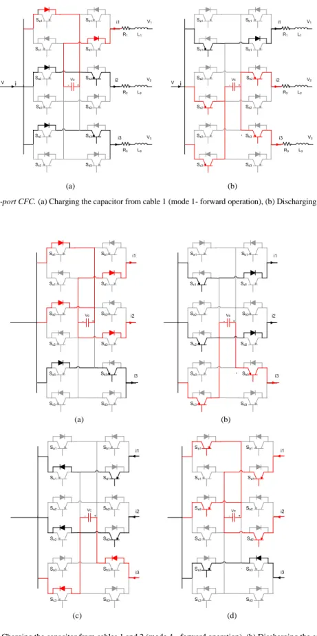
Sa1 Sb1 Sc1 Sd1 Sa2 Sb2 Sc2 Sd2 Sa3 Sb3 Sc3 Sd3 i1 i2 i3 Vc + -Sa1 Sb1 Sc1 Sd1 Sa2 Sb2 Sc2 Sd2 Sa3 Sb3 Sc3 Sd3 i1 i2 i3 Vc + -R1 L1 V1 R2 L2 V2 R3 L3 V3 R1 L1 V1 R2 L2 V2 R3 L3 V3 i V i V (a) (b)
Fig. 1. Proposed extended three-port CFC. (a) Charging the capacitor from cable 1 (mode 1- forward operation), (b) Discharging the capacitor in cables 2 and 3 (mode 1- forward operation).
Sa1 Sb1 Sc1 Sd1 Sa2 Sb2 Sc2 Sd2 Sa3 Sb3 Sc3 Sd3 i1 i2 i3 Vc + -Sa1 Sb1 Sc1 Sd1 Sa2 Sb2 Sc2 Sd2 Sa3 Sb3 Sc3 Sd3 i1 i2 i3 Vc + (a) (b) Sa1 Sb1 Sc1 Sd1 Sa2 Sb2 Sc2 Sd2 Sa3 Sb3 Sc3 Sd3 i1 Vc + -Sa1 Sb1 Sc1 Sd1 Sa2 Sb2 Sc2 Sd2 Sa3 Sb3 Sc3 Sd3 Vc + -i2 i3 i1 i2 i3 (c) (d)
Fig. 2. CFC conduction states. (a) a Charging the capacitor from cables 1 and 2 (mode 4 - forward operation), (b) Discharging the capacitor in cable 3(mode 4 - forward operation), (c) Charging the capacitor from cable 3(mode 9 - reverse operation), (d) Discharging the capacitor in cables 1 and 2 (mode 9- reverse operation).
B. Modes of operation
The basic idea of the CFC is to use the capacitor to transfer energy from the cables carrying current higher than the average value to the cables that carries low current. This action results in balancing the current in the cables connected to the CFC. There are many modes of operation for the proposed CFC depending on the cable current directions and magnitudes. The following subsections discuss the switching states of the proposed three-port CFC for different modes of operation.
Fig. 1(a) and Fig. 1(b) illustrate the three-port CFC operation in the forward direction, where the currents are assumed to be outgoing from the CFC. In this case, two modes are considered. The first mode where one cable carries the highest current while the currents of the other cables are lower than the average value of the three cable currents. In the second mode, two cables are carrying currents higher than the balanced value. For mode 1, assuming i1 is the highest current, switches Sb2 and Sb3 are
turned-on during the charging period to allow for the currents i2
and i3 to flow directly in their cables, while cable 1 is connected
to the capacitor through the feedback diodes of Sa1 and Sd1, as
shown in Fig. 1(a). As a result, i1is reduced by charging the
capacitor. In the discharging period of the capacitor, switches Sc2
and Sc3 are turned-on to insert the capacitor to cables 2 and 3
with reverse polarity, as shown in Fig. 1(b). This action is similar to introducing opposite voltage source to these cables. In addition, Sc1 is turned-on to allow the flow of i1 in its cable. The
charging and discharging states are kept interchanging to transfer of power from cable 1 to cables 2 and 3. This mode of operation is useful when cable 1 is carrying much more current and it is needed to redistribute it among the other two cables. Another mode of operation is where two cables, 1 and 2 for example, are carrying high currents and it is required to transfer power from these cables to cable 3 (mode 4). In charging state, the capacitor is charging from cables 1 and 2 through the feedback diodes of Sa1, Sd1 and Sa2, Sd2, respectively. Moreover,
switch Sb3 is turned-on to allow the flow of i3 directly in its cable,
as indicated in Fig. 2(a). During the discharging state, switches Sc1, Sc2 and Sc3 are turned-on to transfer energy stored in the
capacitor from cables 1 an 2 to cable 3 as shown in Fig. 2(b). Another scenario is when the three cable currents are reversed in direction to go into the CFC from the right side, as illustrated in Fig. 2(c) and Fig. 2(d). All the switching sequence discussed for modes 1 to 6 of the forward direction are changed. Modes 7 to 12 are similar to modes 1 to 6, but the currents are reversed. For mode 9, if i3 is the highest current magnitude,
switches Sd1 and Sd2 are turned-on to bypass their currents and
the capacitor is charged from cable 3 as demonstrated in Fig. 2(c). During the discharge state, the capacitor with reverse polarity is inserted in cables 1 and 2 by turning-on Sa1 and Sa2,
respectively, as shown in Fig. 2(d). In addition, Sa3 is turned-on
to allow the flow of i3 in its cable. Similarly, the previous
switching algorithm can be modified so that currents can be transferred from any desired cable(s) to the remaining cable(s).
Based on the previous discussion of the different modes of operation of the proposed three-port CFC, the switching states for different conditions of the cable currents are shown in Table 1. The second column of Table 1, includes the currents with magnitudes higher than the average value of the three cables
originate from the CFC. As indicated, three possibilities for the highest current at each mode and hence, a total of twelve switching states are presented.
III. MATHEMATICAL MODELLING
This section presents the dynamic model of the proposed three-port CFC using averaging technique where the terminals voltages are taken into consideration as setting values. Fig. 1(a) and (b) illustrate the circuit diagrams of the three-port CFC for the charging and discharging operation mode 1. The following set of equations describes the circuit of Fig. 1(a) when the capacitor is charging from the line carrying the highest current, i1. 𝑉 = 𝑟1𝑖1+ 𝐿1 𝑑𝑖1 𝑑𝑡 + 𝑣𝑐+ 𝑉1 (1) 𝑉 = 𝑟2𝑖2+ 𝐿2 𝑑𝑖2 𝑑𝑡 + 𝑉2 (2) 𝑉 = 𝑟3𝑖3+ 𝐿3 𝑑𝑖3 𝑑𝑡 + 𝑉3 (3) 𝑖1= 𝐶 𝑑𝑣𝑐 𝑑𝑡 (4)
where 𝑟𝑥 𝑎𝑛𝑑 𝐿𝑥 are the resistance and the inductance of the
line number 𝑥 originates from the CFC bus and carrying an instantaneous current 𝑖𝑥, 𝑣𝑐is the capacitor voltage, V is the
voltage at the bus where the CFC is connected to , 𝑉1, 𝑉2 𝑎𝑛𝑑 𝑉3
are the voltages at the end terminals of the first, second, and third lines, respectively. By defining 𝑥𝑇 = [𝑖
1 𝑖2 𝑖3 𝑣𝑐] as state
vector, where the super-suffix T refers to the transpose operation, equations (1), (2), (3), and (4) can be arranged in matrix form as:
[ 𝐿1 0 0 0 0 𝐿2 0 0 0 0 𝐿3 0 0 0 0 𝐶 ] ⏟ 𝐾 𝑑 𝑑𝑡[ 𝑖1 𝑖2 𝑖3 𝑣𝑐 ] ⏟ 𝑋̇ = [ −𝑟1 0 0 −1 0 −𝑟2 0 0 0 0 −𝑟3 0 1 0 0 0 ] ⏟ 𝐴1 [ 𝑖1 𝑖2 𝑖3 𝑣𝑐 ] ⏟ 𝑋 + [ 1 −1 0 0 1 0 −1 0 1 0 0 −1 0 0 0 0 ] ⏟ 𝐵1 [ 𝑉 𝑉1 𝑉2 𝑉3 ] ⏟ 𝑈 (5)
Similarly, the state equations of Fig. 1(b), where the capacitor is discharging into the two other lines carrying currents i2 and i3, are as follows:
[ 𝐿1 0 0 0 0 𝐿2 0 0 0 0 𝐿3 0 0 0 0 𝐶 ] ⏟ 𝐾 𝑑 𝑑𝑡[ 𝑖1 𝑖2 𝑖3 𝑣𝑐 ] ⏟ 𝑋̇ = [ −𝑟1 0 0 0 0 −𝑟2 0 1 0 0 −𝑟3 1 0 −1 −1 0 ] ⏟ 𝐴2 [ 𝑖1 𝑖2 𝑖3 𝑣𝑐 ] ⏟ 𝑋 + [ 1 −1 0 0 1 0 −1 0 1 0 0 −1 0 0 0 0 ] ⏟ 𝐵2 [ 𝑉 𝑉1 𝑉2 𝑉3 ] ⏟ 𝑈 (6)
Assume the duty ratio of the charging mode of operation is D. Multiplying (5) and (6) by D and (1-D), respectively, and adding the results to obtain the average model for the CFC for mode 1 as follows:
[ 𝐿1 0 0 0 0 𝐿2 0 0 0 0 𝐿3 0 0 0 0 𝐶 ] ⏟ 𝐾 𝑑 𝑑𝑡[ 𝑖1 𝑖2 𝑖3 𝑣𝑐 ] ⏟ 𝑋̇ [ −𝑟1 0 0 −𝐷 0 −𝑟2 0 1 − 𝐷 0 0 −𝑟3 1 − 𝐷 𝐷 −1 + 𝐷 −1 + 𝐷 0 ] ⏟ 𝐴 [ 𝑖1 𝑖2 𝑖3 𝑣𝑐 ] ⏟ 𝑋 + [ 1 −1 0 0 1 0 −1 0 1 0 0 −1 0 0 0 0 ] ⏟ 𝐵 [ 𝑉 𝑉1 𝑉2 𝑉3 ] ⏟ 𝑈 (7)
where A=DA1+(1-D)A2 and B=DB1+(1-D)B2. At steady
state, (7) is written as [ −𝑟1 0 0 −𝐷 0 −𝑟2 0 1 − 𝐷 0 0 −𝑟3 1 − 𝐷 𝐷 −1 + 𝐷 −1 + 𝐷 0 ] ⏟ 𝐴 [ 𝐼1 𝐼2 𝐼3 𝑉𝑐 ] ⏟ 𝑋 + [ 1 −1 0 0 1 0 −1 0 1 0 0 −1 0 0 0 0 ] ⏟ 𝐵 [ 𝑉 𝑉1 𝑉2 𝑉3 ] ⏟ 𝑈 = 0 (8)
where I1, I2, I3, and Vc are the steady state values of 𝑖1, 𝑖2, 𝑖3,
and 𝑣𝑐, respectively. Solving (8), the steady state value of
capacitor voltage is obtained as
𝑉𝑐 = 𝐷(𝑉−𝑉1)−𝑟1(1−𝐷){𝑉−𝑉2𝑟2 +𝑉−𝑉3𝑟3 } 𝐷2+𝑟1(1 𝑟2+ 1 𝑟3)(1−𝐷)2 (9)
Equation (9) gives an expression for the capacitor voltage as a function of the network parameters and the voltage drops across the cables connected to the CFC which represents the loading condition of the grid. It is worth mentioning that the
rated voltage of the CFC switches, which is equal to the rated capacitor voltage, can be estimated from (9).
In order to calculate the capacitor voltage ripple, (5) is integrated over the charging period as follows:
∫ 𝑖1
𝐷𝑇
0 𝑑𝑡 = 𝐶 ∫ 𝑣𝑐
𝑉𝑐𝑚𝑎𝑥
𝑉𝑐𝑚𝑖𝑛 (10)
where T refers to the switching period which is the reciprocal of the switching frequency fs. Neglecting the current ripples
compared to the average value, I1, results in linear charging of
the capacitor from initial minimum voltage Vcmin to maximum
voltage Vcmax. Therefore the capacitor voltage ripple, ∆𝑉𝑐 can be
estimated from (10)
∆𝑉𝑐= 𝑉𝑐𝑚𝑎𝑥− 𝑉𝑐𝑚𝑖𝑛=
𝐷 𝐼1
𝐶 𝑓𝑠 (11)
It can be seen from (11) that increasing the capacitance reducing the capacitor voltage ripple, as expected. As can be seen from (8), the parameters of the DC grid and loading condition influence the line current which affects the capacitor voltage ripple. Moreover, the capacitor voltage ripple depends on the mode of operation as the charging current, which is I1 for
mode 1, changes from mode to another. For mode 1, the capacitance can be roughly estimated from (9) and (11) to meet a required percentage voltage ripple, ∆𝑉𝑐 𝑝𝑢= ∆𝑉𝑐/𝑉𝑐, at the
extreme deviations of the line currents. In a similar way, the capacitance can be calculated for each mode of operation for the CFC. Finally, the maximum value of the capacitance is considered to meet the desired level of voltage ripple for all modes of operation. In this paper, the capacitance of the CFC is selected using trial and error since the practical limitations of the DC grid under study are not considered.
TABLE I CFC SWITCHING STATES
Mode Currents Direction Switching states
Sa1 Sa2 Sa3 Sb1 Sb2 Sb3 Sc1 Sc2 Sc3 Sd1 Sd2 Sd3 1 2 3 4 5 6 7 8 9 10 11 12 i1 i2 i3 i1 & i2 i2 & i3 i1 & i3 i1 i2 i3 i1 & i2 i2 & i3 i1 & i3 Forward Forward Forward Forward Forward Forward Reverse Reverse Reverse Reverse Reverse Reverse off off off off off off pulsed pulsed pulsed pulsed pulsed pulsed off off off off off off pulsed pulsed pulsed pulsed pulsed pulsed off off off off off off pulsed pulsed pulsed pulsed pulsed pulsed off on on off on off off off off off off off on off on off off on off off off off off off on on off on off off off off off off off off pulsed pulsed pulsed pulsed pulsed pulsed off off off off off off pulsed pulsed pulsed pulsed pulsed pulsed off off off off off off pulsed pulsed pulsed pulsed pulsed pulsed off off off off off off off off off off off off off on on off on off off off off off off off on off on off off on off off off off off off on on off on off off
TABLE II
REAL TIME SIMULATION PARAMETERS
Element Value Time step Grid voltage Capacitor 25uS 320kV 10mF Cable 1-2 Cable 1-3 Cable 1-4 Cable 2-3 Cable 3-4 1.42Ω &0.021H 2.42Ω &0.021H 2.42Ω &0.021H 2.42Ω &0.021H 2.42Ω &0.021H i2 + + 1 3 + -HCC Hysteresis band current
controller
User input value for: - current nulling -current setting value
ix i*(reference) (measured) PWM to relevant IGBT (Sc1, Sc2 and Sc3 or Sa1, Sa2 and Sa3)
Reference signal for currents balancing function i1 HB user input ON / OFF i3 + Fig. 3. Proposed HCC controller.
IV. CONTROL STRATEGIES
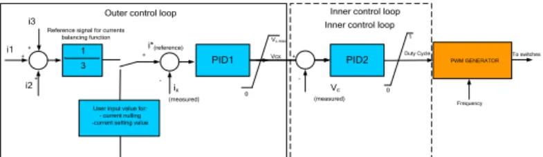
To achieve the proposed modes of operation discussed earlier accurately, two proposed control strategies based on Hysteresis Current Control (HCC) and Proportional Integral (PI) controller are shown in Fig. 3 and Fig. 4 respectively. For currents balancing, the sum of the three currents is calculated and divided by their number to obtain the reference current i*. The calculated reference current is then compared by the actual measured current ixand the error signal is minimized by using
either HCC or PI controller. For other functions such as currents limiting and nulling, the reference value is set directly by the user. In some cases where it is required to limit the CFC capacitor voltage as an over voltage protection procedure, Fig.5 shows two cascaded control loops, where one control the currents and the other aims for voltage regulation.
V. SIMULATION CASE STUDIES
Real time simulation is carried out using OP4510 real time simulator and programmed using MATLAB/SIMULINK software package in this section. A four terminals DC grid is simulated to evaluate the dynamic and steady state performance of the proposed three-port CFC. The simulation parameters are shown in table II. Three case studies are presented in the following subsections to evaluate the different features and operation modes of the proposed CFC.
i2 + + 1 3 + -PID1
User input value for: - current nulling -current setting value
ix i*(reference)
Vcx Reference signal for currents
balancing function i1 PWM GENERATOR Frequency Duty Cycle Vc -+ Vc.max 0 1 0 (measured)
Inner control loop
PID2
Inner control loop Outer control loop
To switches
(measured) +
i3
Fig. 4. Proposed PID cascaded controllers for a three ports CFC.
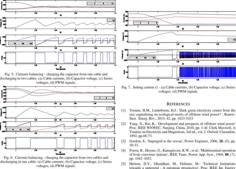
A. Charging from cable 1 and discharging in cables 2 and 3 In this case study, currents i1, i2 and i3 are equal to 0.7kA, 0.42kA and 0.43kA, respectively. It is required to redistribute the currents to achieve a balanced operation by decreasing the current flow in cable 1 and increase the currents flow in cable 2 and 3. The proposed control selects mode one of operation for the CFC which is programed to activated at t = 1 seconds. Fig. 5(a) demonstrates that the proposed three-port CFC succeeds to balance the three cable currents with fast dynamics and without overshoot. Fig. 5(b) illustrates the capacitor voltage which is less than 500 volts. This result proves one of the advantages of the proposed CFC that is the capacitor and switches voltage rating is very small when compared to the grid voltage 320kV. The series voltage introduced by the CFC to each cable is shown in Fig. 5(c). Notice that series voltage of cables 2 and 3 are the same. Finally, Fig. 5(d) shows the generated PWM signal in this case.
B. Charging from cables 1 and 3 and discharging in 2 In this case study, currents i1 and i3 are higher than i2 and the average value. Mode 2 is activated to redistribute the currents among the cables at t = 1 seconds. Fig. 6(a) indicate the successful action of the proposed CFC to decrease both i1 and i3 from 1.1kA and 1kA, and simultaneously increasing i2 from 0.42kA to achieve a balanced operation at approximately 0.5kA. Fig. 6(b) displays the capacitor voltage at this case while Fig. 6(c) and 6(d) show the series voltages and PWM signal respectively.
C. Current set point
The final simulation case study is dedicated to test the feature of the proposed CFC to set any cable current to a desired value. In this case, current i1 is equal to 1.1kA, initially, and is required to reduce it to 0.25kA. The CFC controller is enabled at t = 1 seconds. It can be noted from Fig. 7(a) that the CFC succeeds in achieving this target smoothly. The capacitor voltage at this case is shown in Fig. 7(b). It is worth mentioned that the capacitor voltage for this case is higher than the previous cases. This action is expected as to achieve the required reduction in one cable current, the capacitor should be charged to a higher level of voltage of 1kV compared to the current balancing cases. As explained in section 3.1, the capacitor is inserted to the other two cables to transfer the energy from cable 1. Fig. 7(c) and Fig. 7(d) show both series voltages and PWM signal for this case respectively.
Fig. 5. Currents balancing - charging the capacitor from one cable and discharging in two cables. (a) Cable currents, (b) Capacitor voltage, (c) Series
voltages, (d) PWM signals.
Fig. 6. Currents balancing - charging the capacitor from two cables and discharging in one cable. (a) Cable currents, (b) Capacitor voltage, (c) Series
voltages, (d) PWM signals.
VI. DISCUSSION
The presented simulation results explore the fast dynamic response and accurate performance of the proposed CFC. It is noticed that the capacitor voltages are relatively low when compared to grid voltage, which is reflected in low rating and cost CFC capacitor and IGBTs. However, the proposed topology may fail to control currents when the difference in magnitude between them is high, as this topology has single capacitor and it controls both currents simultaneously.
VII.CONCLUSION
This paper presents the dynamic modelling and principle of operation for an extended topology of an IGBT based current flow controller. The proposed CFC can be used for the power and current flow control applications in DC grids including multi-terminal HVDC systems. Features such as currents balancing, current limiting, and current nulling of the proposed extended three-port CFC are discussed and evaluated. Precise performance of the proposed system is explored using OP4510 real time simulator. Results revealed that the proposed extended topology may a way out for futuristic DC grids current flow control problems.
Fig. 7. Setting current i1 - (a) Cable currents, (b) Capacitor voltage, (c) Series voltages, (d) PWM signals.
REFERENCES
[1] Toonen, H.M., Lindeboom, H.J.: 'Dark green electricity comes from the
sea: capitalizing on ecological merits of offshore wind power? ', Renew. Sust. Energ. Rev., 2015, 42, pp. 1023-1033
[2] Yang, X., Bai, K.: 'Development and prospects of offshore wind power'
Proc. IEEE WNWEC, Nanjing, China, 2010, pp. 1-4J. Clerk Maxwell, A Treatise on Electricity and Magnetism, 3rd ed., vol. 2. Oxford: Clarendon, 1892, pp.68-73.
[3] Gordon, S.: 'Supergrid to the rescue', Power Engineer, 2006, 20, (5), pp. 30-33.
[4] Foerst, R., Heyner, G., Kanngiesser, K.W., et al.: 'Multiterminal operation of hvdc converter stations', IEEE Trans. Power App. Syst., 1969, 88, (7), pp. 1042–1052.
[5] Hertem, D.V., Ghandhari, M., Delimar, M.: 'Technical limitations
towards a supergrid - A european prospective', Proc. IEEE Int. Energy Conf. Exhib., Manama, Bahrain, Dec. 2010, pp. 302-309.
[6] Shukla, A., Demetriades, G.D.: 'A Survey on hybrid circuit-breaker topologies', IEEE Trans. On Power Deliv., 2015, 30, (2),pp. 627-641
[7] Barker, C.D., Whitehouse, R.S.: 'An alternative approach to HVDC grid
protection', 9th IET Int. Conf. on AC and DC Pow. Transm., Birmingham, UK, Dec. 2012, pp. 1-6
[8] Sneath, J., Rajapakse, A.D.: 'fault detection and interruption in an earthed HVDC grid using ROCOV and hybrid DC breakers', IEEE Trans. Power Del., 2014, PP, (99) pp. 1-8
[9] Sada Jovcic, D.: 'Bidirectional, high-power dc transformer', IEEE Trans. on Power Deliv., 2009, 24, (4), pp. 2276-2283
[10] Carrizosa, M.J., Navas, F.D., Damm, G., et al.: 'Optimal power flow in
multi-terminal HVDC grids with offshore wind farms and storage devices', Int. Journal of Elec. Power & Energy Sys. , 2015, 65, pp. 291– 298.
[11] Diab, H.Y., Marei, M.I. , Tennakoon, S.B. "An investigation of power flow control methods in multi terminal high voltage DC grids." Power Engineering Conference (UPEC), 2015 50th International Universities. IEEE, 2015.
[12] Diab, H.Y., Marei, M.I. , Tennakoon, S.B. "Operation and control of an insulated gate bipolar transistor-based current controlling device for power flow applications in multi-terminal high-voltage direct current grids." IET Power Electronics, 2016, 9, (2), pp. 305-315.
[13] Barker, C.D., Whitehouse, R.S.: 'A current flow controller for use in HVDC grids', 10th IET international Conf. on AC and DC Pow. Transm., Birmingham, UK, 2012, pp. 1-6.