HIGH PERFORMANCE LOOP FILTER DESIGN FOR CONTINUOUS-TIME SIGMA-DELTA ADC
A Thesis by FAN GUI
Submitted to the Office of Graduate and Professional Studies of Texas A&M University
in partial fulfillment of the requirements for the degree of MASTER OF SCIENCE
Chair of Committee, Jose Silva-Martinez Committee Members, Aydin Karsilayan
Peng Li Javier Jo Head of Department, Chanan Singh
December 2014
Major Subject: Electrical Engineering
ii ABSTRACT
Continuous-time (CT) sigma-delta (Σ∆) analog-to-digital converters (ADCs) are widely used in wireless transceiver. Loop filter becomes a critical component in the implementation of high resolution large bandwidth CT Σ∆ ADC because it determines loop stability and defines quantization noise-shaping behavior of the Σ∆ modulator.
In this thesis, an extremely low power loop filter for 11-bit dynamic range 15MHz CT Σ∆ ADC is described. On the system level, a new local feedback structure which consists of a CT differentiator in cascade with an integrator is proposed to solve the problem of excess loop delay and eliminate the use of a power-hungry summing amplifier. Proposed continuous-time differentiator is demonstrated to make the whole Σ∆ loop more robust to delay variation and easier designed than previously published discrete-time differentiator. On the circuit level, two-stage operational amplifiers with new class-AB output stages are used to implement low-power active RC integrators. The proposed class-AB output stage is proven to be more linear than conventional one. The whole Σ∆ ADC circuit was designed, simulated and implemented in IBM 130nm CMOS technology. The designed loop filter including CT differentiator draws less than 3mA from 1.2V supply voltage.
iii
ACKNOWLEDGEMENTS
I would like to thank my parents for allowing me to chase dreams. All the support they have provided me over the years was the greatest gift anyone has ever given.
Next, I need to thank my supervisor, Dr. Jose Silva-Martinez who is always patient with me. I still remember my 1st time to get in touch with real integrated circuit design. It was for a research project. The weekly meetings with Dr. Silva usually lasted for more than 2 hours in the beginning, and they were like one on one instructions. But he never complained.
Thanks also go to my roommates, Cheng Zhu and Xi Jiang. We had a great time at College Station. I need to further thank my officemates, Younghoon and Noah who always took time to listen. I would like to thank all my friends, particularly Yaoqi Niu, Shengchang Cai and Qiyuan Liu who gave me a lot of hints when I was preparing for job interviews. Without your help, I couldn’t land a career in analog design.
I would also like to acknowledge my committee members, Dr. Peng Li, Dr. Karsilayan and Dr. Javier for their guidance and support throughout the course of this research.
Finally, I would like to thank my group fellows, Alexander, Negar and Carlos. It’s my honor to work with such brilliant people.
iv TABLE OF CONTENTS Page ABSTRACT ... ii ACKNOWLEDGEMENTS ... iii TABLE OF CONTENTS ... iv LIST OF FIGURES ... vi LIST OF TABLES ... ix CHAPTER I INTRODUCTION ... 1 Motivation ... 1 Thesis Organization... 3
CHAPTER II OVERVIEW OF SIGMA DELTA ADC ... 5
Analog-to-digital Conversion ... 5
Oversampling-rate ADC ... 8
Oversampled Noise-shaping Converters: Sigma-delta ADC ... 11
Continuous-time and Discrete-time Sigma-delta Modulators ... 14
Performance Parameters of Sigma-delta Modulators ... 16
Non-idealities in Continuous-time Sigma-delta Modulator ... 17
CHAPTER III DESIGN OF CONTINUOUS-TIME SIGMA-DELTA MODULATOR ... 22
Background ... 22
System Level Design Considerations ... 24
Sigma-delta Loop Transfer Function ... 24
Modulator Loop Topology ... 26
Proposed Modulator Architecture ... 27
CHAPTER IV DESIGN OF 3RD ORDER LOW-PASS LOOP FILTER ... 31
Background ... 31
Active RC Integrator ... 32
v
Loop Filter Architecture ... 35
Opamp Design Considerations ... 36
A Linear Class AB Amplifier... 40
Simulation Results ... 45
CHAPTER V CONTINUOUS-TIME DIFFERENTIATOR ... 53
Discrete-time Differentiator ... 53
Continuous-time Differentiator ... 59
CHAPTER VI CONCLUSION ... 70
vi
LIST OF FIGURES
Page
Figure 1 Basic diagram of a direct conversion wireless receiver ... 1
Figure 2 Quantization error for a 3bit ADC ... 7
Figure 3 Properties of the quantization error in white noise model ... 8
Figure 4 A/D conversion architectures ... 9
Figure 5 Illustration of spectral effect of oversampling ... 10
Figure 6 Block diagram of sigma delta modulator ... 11
Figure 7 Typical STF and NTF plot for a low-pass sigma-delta modulator ... 12
Figure 8 Discrete-time and continuous-time sigma-delta modulator ... 14
Figure 9 Block diagram of CT 𝚺∆ ADC with excess loop delay ... 21
Figure 10 Local feedback technique ... 22
Figure 11 System-level model of our CT sigma delta modulator ... 25
Figure 12 Impulse response of main path in s domain and z domain ... 26
Figure 13 A 3rd order CT Low pass 𝚺∆ ADC with feed-forward architecture ... 28
Figure 14 Proposed CT sigma delta ADC architecture ... 29
Figure 15 Active RC integrator ... 32
Figure 16 Capacitor tuning mechanism for integrator ... 34
Figure 17 Biquadratic filter ... 34
Figure 18 3rd order loop filter ... 36
Figure 19 Opamp in feedback ... 37
Figure 20 Closed loop and open loop of 1st integrator ... 38
Figure 21 Large output swing class-AB CMOS output stage with CM transistor coupling ... 40
vii
Figure 22 Two-stage opamp with class AB output ... 41
Figure 23 Proposed class AB output stage ... 42
Figure 24 Schematic of linear class AB amplifier ... 43
Figure 25 CMFB for proposed linear class AB amplifier ... 44
Figure 26 Layout of 3rd order loop filter ... 45
Figure 27 Noise performance of 1st opamp ... 46
Figure 28 Loop gain of 1st opamp ... 47
Figure 29 Linearity test schematic ... 48
Figure 30 IM3 for conventional and proposed class AB amplifier ... 48
Figure 31 IPN curve for conventional and proposed class AB amplifier ... 49
Figure 32 CMFB simulation result ... 50
Figure 33 AC response of biquad filter ... 51
Figure 34 Noise performance of 3rd loop filter ... 52
Figure 35 Conventional differentiator used in CT 𝚺∆ ADC ... 54
Figure 36 System-level model of CT 𝚺∆ modulator with DT differentiator ... 54
Figure 37 Signal chain of DT differentiator in cascade with integrator ... 55
Figure 38 Pulse response interpolation of DT differentiator in cascade with integrator (sampling cycle is normalized to 1) ... 56
Figure 39 Equivalent fast path output waveform with ELD variation ... 57
Figure 40 Pulse response interpolation of DT differentiator in cascade with integrator given 10% ELD variation (sampling cycle is normalized to 1) ... 58
Figure 41 Root locus of NTF vs ELD variation for DT differentiator ... 59
Figure 42 Proposed differentiator in cascade of integrator ... 60
viii
Figure 44 Pulse response interpolation of CT differentiator in cascade with integrator
(sampling cycle is normalized to 1) ... 62
Figure 45 ELD variation in proposed fast path DAC ... 62
Figure 46 Pulse response interpolation of CT differentiator in cascade with integrator given 10% ELD variation (sampling cycle is normalized to 1) ... 63
Figure 47 Root locus of NTF vs ELD variation for CT differentiator ... 64
Figure 48 SNR and SFDR performance for SDM with CT/DT differentiator ... 65
Figure 49 Schematic of differentiator ... 66
Figure 50 Chip micrograph of CT 𝚺∆ ADC ... 67
ix
LIST OF TABLES
Page Table 1 System level design parameters for low-pass 𝚺∆ ADC ... 30 Table 2 Trans-conductance needed for each opamp in terms of linearity ... 39 Table 3 Summary of linearity performance ... 49 Table 4 Performance summary of designed 3rd order loop filter for CT 𝚺∆ modulator .. 69
1 CHAPTER I INTRODUCTION
Motivation
The recent technological growth in the wireless communication industry indicates a strong need for high performance analog-to-digital converters (ADC). Figure 1 shows the basic diagram of a popular direct conversion wireless receiver.
LNA RF Filter VGA BB Filter Mixer Digital Circuit ADC
Figure 1 Basic diagram of a direct conversion wireless receiver
Sigma-Delta (Σ∆) modulator ADCs are used most exclusively in wireless applications for a number of reasons. Firstly, thanks to the advances of both the semiconductor technology and the design techniques, the input signal bandwidth which Σ∆ ADCs can handle is extended to the MHz range. Secondly, over-sampling characteristic of the Σ∆ ADCs generally reduces the performance requirement of the anti-aliasing filters (e.g., BB filter in Figure 1), which are power-hungry blocks in wireless receivers. Thus, Σ∆ ADCs are very suitable for low-power design, which is one of the most important concerns in the battery-powered wireless equipment (e.g., mobile phones).
2
Thirdly, Σ∆ ADCs spectrally shape most of the analog circuit error away from the band of interest, to achieve accuracy only in a narrow band. Out-of-band noise and distortion would be filtered out by following digital circuits. A relatively narrow signal bandwidth of Σ∆ ADC, matches the usual case that the bandwidth of an analog signal of interest in a wireless receiver is much narrower compared with practical data-converter sampling rates and digital filter clock rates.
Previously commercial Σ∆ ADCs for wireless communications (e.g., GSM and WCDMA) were implemented by using switch-capacitor techniques [1] [2], which are also known as discrete-time (DT) Σ∆ ADCs mainly due to mature design methodologies and robustness. The bandwidth of DT Σ∆ ADC, however, is usually limited to several hundred kHz. Applications, like WLAN and LTE, demand a much wider bandwidth ADC that can digitize both the desired and adjacent-channel interferes, resulting in a high dynamic range requirement. Increasingly continuous time (CT) Σ∆ ADCs were reported [3] [4] [5] [6]recently, and showed impressive performance to satisfy this requirement.
In the design of high performance Σ∆ ADC, the use of analog filters is unavoidable. The transfer function of loop filter defines the quantization noise-shaping behavior. The stability of Σ∆ ADC mainly depend on the locations of poles and zeros in the loop filter. Hence, the loop filter becomes a critical part in Σ∆ ADC.
One of main problems that wide bandwidth CT Σ∆ ADCs face is excess loop delay. Excess loop delay changes equivalent z domain loop transfer function characteristic and affects the stability and dynamic range performance [7]. In conventional CT Σ∆ ADCs local feedback technique [3] turns out indispensable to compensate excess loop delay and
3
help achieve a wide signal bandwidth. This technique, however, demands a power-hungry summing amplifier.
In this thesis, a differentiation operation is introduced in the local feedback path, which allows the signal to be fed to the input of the last integrator of loop filter. Thus, the summing amplifier is removed, and power is saved. Our proposed continuous-time differentiator is demonstrated to make the whole loop more robust to excess loop delay variation, and easier to be designed than previously published discrete-time differentiator [4]. Moreover, a new linear class AB output stage is used to improve the linearity of conventional class AB amplifier and increase current efficiency of loop filter for CT Σ∆ modulator.
The target of this thesis is to design an extremely low power loop filter with a new local feedback structure for 15MHz low-pass Σ∆ ADC to achieve 11bit dynamic range.
Thesis Organization
This thesis covers system-level and circuit-level analysis of loop filter for CT Σ∆ ADC. After describing the design issues of the CT Σ∆ ADC, the detailed design procedure of a prototype loop filter is presented. The thesis is organized as follows:
Chapter 1 provides a brief introduction to application of ADC in wireless receiver. A brief note on advantages of CT Σ∆ ADC is presented. The importance of loop filter in the design of high performance CT Σ∆ modulator is identified.
In Chapter 2, an overview of analog-to-digital conversion and basic knowledge of sigma-delta modulator are presented. The architectural difference between
continuous-4
time and discrete-time Σ∆ modulators are discussed. Various performance parameters and circuit non-ideality of Σ∆ ADCs are described.
In Chapter 3, several system-level design considerations of CT Σ∆ ADC are discussed. The power-hungry summing amplifier is identified, and a revised loop filter architecture is proposed to improve power efficiency.
Chapter 4 and Chapter 5 present detailed circuit level analysis of this proposed loop filter architecture and amplifier implementation. Abundant simulation results are given to support the theory.
5 CHAPTER II
OVERVIEW OF SIGMA DELTA ADC
This chapter is intended to give an introduction and overview of analog-to-digital conversion; first in general and, thereafter, for the basic operation of sigma delta modulator. Structure differences between continuous-time and discrete-time sigma delta ADCs are identified. Many system-level implementation issues are brought to discussion. Various design parameters of sigma-delta ADCs are present.
Analog-to-digital Conversion
The conversion of analog signal to digital output can simply be separated into two basic processes: sampling in time and quantization in amplitude.
Sampling an analog signal in time domain is equal to multiply the signal by an ideal impulse train spaced by Ts. Ts is the sampling period. In time domain, the sampling process of a continuous-time signal Xc(t) that produces a sampled output signal Xs(t) is given by the following equation,
Xs(𝑡) = ∑ 𝑋𝑐(𝑡)𝛿(𝑡 − 𝑛𝑇𝑠) ∞
𝑛=−∞
(2.1)
where n is an integer and δ(t) is the Dirac delta function. Further, the frequency domain representation of equation (2.1) can be obtained as follows,
Xs(𝑓) = 𝑋𝑐(𝑓) ∑ 1
𝑇𝑠𝛿(𝑓 − 𝑛𝑓𝑠)
∞
𝑛=−∞
6
where X(f) represents the Fourier transform of X(t) and fs is the sampling frequency, inverse of Ts . Based on equation (2.2), it can be seen that sampling operation mathematically results in periodic reproduce of the original signal spectrum at multiples of fs.
To avoid spectrum alias and recover the original signal, the minimum sampling frequency is required to be twice the maximum signal frequency component or signal bandwidth. This sampling frequency is also referred as the Nyquist sampling rate which is given by
fnyquist = 2𝑓𝑠𝑖𝑔_𝑏𝑤 (2.3)
An ADC working with a sampling frequency of fnyquist is called a Nyquist Rate converter. The process of quantization in amplitude, usually referred to as quantization, encodes a continuous range of analog values into a set of discrete levels. Since the sampled analog signal is mapped into a finite number of output amplitude values, even ideal quantization process introduces errors into signal. These errors are defined as a quantization error. The main job of ADC design is to limit quantization errors.
The most important performance metric of a quantizer is its number of bits (NOB). If all output discrete levels are equally distributed, the space between two adjacent ones are defined as the quantizer step width,
∆= 𝐹𝑆
2𝑁𝑂𝐵− 1 (2.4)
7
Consider a signal Xn+ ε is ideally quantized into level Xn, where ε is the quantization error. Basically ε never exceeds an amplitude level equal to ±∆2 since signal larger than Xn+∆2 are quantized to the next quantization level Xn+1. Figure 2 is an
example showing the quantization error vs input amplitude level for a 3bit ideal ADC.
Figure 2 Quantization error for a 3bit ADC
In quantizer white noise model [8], the probability density of quantization error over the quantization interval −∆
2 to + ∆
2 is uniform as shown in Figure 3(a). The
8 1
P
(a) Probability density function (b) Power spectral density
Figure 3 Properties of the quantization error in white noise model
The quantization noise power can be calculated as, 𝛿𝜀2 = ∫ 𝜀2𝑝𝑑𝑓 𝜀𝑑𝜀 ∞ −∞ = ∆2 12 (2.5) Note that the total quantization error power is independent of the sampling frequency and is only determined by quantization resolution. Since the signals after the quantizer are sampled signals, all the quantization noise power 𝛿𝜀2 is folded into the frequency range
[-fs/2, fs/2]. Thus, with the white noise approximation in Figure 3(b) the power spectral density of the quantization noise is
𝑃𝜀(𝑓) =∆122𝑓𝑠1 (2.6)
Oversampling-rate ADC
Generally ADCs are classified into two kinds, Nyquist-rate and oversampling-rate ADC. A converter with a sampling frequency fs much higher than the Nyquist frequency
9
is called an oversampling converter. Oversampling ratio is defined in terms of sampling frequency and input signal bandwidth as
OSR = 𝑓𝑠 2𝑓𝑠𝑖𝑔𝑏𝑤
(2.7)
The architectures of two converters are presented in Figure 4(a) and 4(b) respectively.
Antialiasing Filter Analog
Input A/D Converter
N bits
Digital Output
Nyqust
F
(a) Nyquist-rate ADC
DAC H(f) Modulator Digital filter N bits Digital Output Analog Input Nyqust F OSR * Antialiasing Filter (b) Oversampling ADC
Figure 4 A/D conversion architectures
The benefit of a high oversampling ratio is twofold [8]. Firstly, the implementation of an antialiasing filter is much easier, because the transition band increases enormously for OSR >>1. More importantly, the power spectral density of the quantization noise
10
reduces proportionally with increasing sampling frequency. It results in lower in-band quantization noise. This is illustrated in Figure 5.
fs fsig_bw fsig_bw fs f X(f) Hanti(f) QNinband
(a) Quantization noise and in-band noise for SOR=1
fs fsig_bw fsig_bw fs f X(f) 2 / fs fs/2 Hanti(f) QNinband
(b) Quantization noise and in-band noise for OSR >>1
Figure 5 Illustration of spectral effect of oversampling
If a digital low-pass filter follows the oversampled converter, all parts outside the bandwidth can be eliminated, leaving only a small part of total quantization noise and
11
boosting signal to noise ratio. The above mentioned digital low-pass filter is usually called the decimation filter.
Oversampled Noise-shaping Converters: Sigma-delta ADC
Oversampling and noise shaping are two key techniques equipped in sigma-delta (Σ∆) ADC. Oversampling reduces the quantization noise floor in signal bandwidth, as discussed in the last section. Sigma delta operation shapes part of in-band quantization noise into out-of-band. The concept diagram of sigma-delta ADC is shown in Figure 6. It is based on a negative feedback loop which consists of a loop filter and quantizer in the feed-forward path, and a digital-to-analog converter (DAC) in the feedback path.
H(z) DAC Loop filter N-bit Quantizer Vin Vout Quantization noise +
-Figure 6 Block diagram of sigma delta modulator
For small signal analysis of sigma-delta modulator, every block is assumed to be linear. H(s) represents the transfer function of loop filter. Quantizer and DAC has a unity
12
gain transfer function. Thus the signal transfer function (STF) and noise transfer function (NTF) of sigma-delta modulator are given in equation (2.8) and equation (2.9) respectively.
STF =𝑉𝑜𝑢𝑡 𝑉𝑖𝑛 = H(z) 1 + H(z) (2.8) NTF = Vout Qnoise = 1 1 + H(z) (2.9) Vout= 𝑆𝑇𝐹 ∗ 𝑉𝑖𝑛+ 𝑁𝑇𝐹 ∗ 𝑄𝑛𝑜𝑖𝑠𝑒 (2.10)
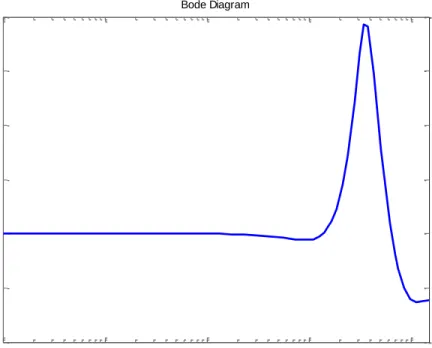
A low pass filter with high in-band gain, H(z), is used for low pass sigma-delta modulator. The plot of typical STF and NTF employing such loop filter are depicted in Figure 7(a) and 7(b) respectively.
(a) Signal transfer function
Figure 7 Typical STF and NTF plot for a low-pass sigma-delta modulator
104 105 106 107 108 -4 -2 0 2 4 6 8 M a g n itu d e ( d B ) Bode Diagram Frequency (Hz)
13
(b) Noise transfer function
Figure 7 Continued
Generally STF is a low-pass function. Input experiences a nearly constant gain for in-band frequency components. NTF is a high-pass function. In-band quantization noise is suppressed considerably while out-of-band quantization noise remains strong. In sum, quantization noise is shaped by sigma delta feedback loop without affecting in-band signal gain. In addition, NTF defines the stability properties of sigma delta modulator [9]. This is the start point of designing high resolution and wide bandwidth sigma-delta ADC.
104 105 106 107 108 -80 -70 -60 -50 -40 -30 -20 -10 0 10 M a g n itu d e ( d B ) Bode Diagram Frequency (Hz)
14
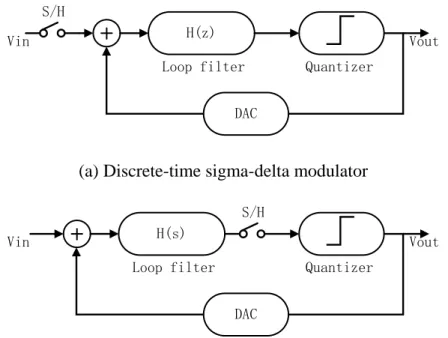
Continuous-time and Discrete-time Sigma-delta Modulators
The sigma-delta modulators are classified into two types based on the location of sample-and-hold (S/H) block. If input signal is sampled before going into sigma-delta loop, the resulting modulator is called discrete-time modulator. And, if sampling operation is performed inside the sigma-delta loop, the resulting architecture is referred as continuous-time sigma-delta modulator. The loop filter of a discrete-continuous-time sigma-delta modulator is implemented with the use of switch-capacitor techniques, and the loop filter of continuous-time sigma-delta modulator is implemented using continuous techniques. The conceptual diagrams of discrete-time and continuous-time sigma-delta architectures are shown in Figure 8(a) and Figure 8(b) respectively.
H(z)
DAC
Loop filter Quantizer S/H
Vin Vout
(a) Discrete-time sigma-delta modulator
H(s)
DAC
Loop filter Quantizer
Vin Vout
S/H
(b) Continuous-time sigma-delta modulator
15
A continuous time modulator is obtained based on a discrete time loop filter. By employing the impulse invariant transformation, a Z domain filter can be mapped into S domain one [7]. Impulse invariant transformation aims at ensuring the open loop response to be equal such that these two modulators behave exactly the same.
In the last two decades switch capacitor (SC) circuits has been the dominant discrete-time (DT) techniques used for implementing the loop filter in SDMS. This was primarily due to the emerging-ease with which monolithic SC filters can be designed, the high degree of linearity of the resulting circuits, and finally the natural allegory between the mathematics of the sigma delta system and the DT circuit-level implementation [8].
However, CT modulator exceed DT competitors in many other aspects. One key advantage of CT modulator is that the sampling operation occurs inside the loop. All non-idealities including sampling error and noise of S/H are shaped by loop gain. In the DT modulator where S/H is placed at the input, all error that this block adds is referred as input error. Besides this noise-suppressed S/H error, the shift of sampling operation behind a continuous-time filter in the forward signal path results in some degree of implicit antialiasing filtering [10].
Furthermore, regarding the opamp bandwidth requirement, continuous time filter design is much more relaxed compared to discrete time counterpart. Generally the amplifiers in SC filters require several time constants to settle, which imposes severe bandwidth requirement at high sampling frequencies [9]. In a CT architecture error introduced by finite gain-bandwidth (GBW) of opamp could be modeled as loop delay, and techniques [11] have proposed to compensate such errors. Over the past few years of
16
research in sigma delta modulator, CT implementation has extended the input bandwidth from kilohertz to megahertz range [3] [5]
Besides all these advantages, CT loop are more difficult to design and simulate. CT components show a higher variation with process, supply-voltage and temperature (PVT). The variation of RC time constant might change the CT filter transfer function, and thus give rise to stability issue [11]. In addition, DAC non-linearity, especially clock jitter induced error, seriously impacts the loop performance for the simple reason that DAC error is added to input and it cannot be suppressed by loop gain [3].
Performance Parameters of Sigma-delta Modulators
The key distinguishing characteristics of sigma-delta modulator includes signal-to-noise-and-distortion-ratio, dynamic range, spurious free dynamic range, signal bandwidth and power consumption.
Signal-to-noise-and-distortion Ratio (SNDR)
SNDR is the ratio of signal power to the noise and all distortion power components. In sigma delta modulator, only in-band noise and distortion accounts to SNDR. However, in practical circuit implementation the performance is degraded by nonlinearity. Intermodulation [12] of higher frequency components like blocker might produce distortions at in-band. Additionally sampling operation can fold out-of-band harmonics in band. To quantify the noise separately another parameter, signal-to-noise ratio (SNR) is used.
17 Dynamic Range (DR)
Dynamic range is defined as the rms voltage of maximum input sinusoidal signal, for which the structure still operates correctly, to the rms voltage of the smallest detectable input sinusoidal. Usually dynamic range implies the effective number of bits (ENOB), or the resolution of sigma delta ADC. The relationship between the dynamic range and resolution of a modulator is given by,
ENOB =DR − 1.76
6.02 (2.11) Note DR is in decibel (dB).
Spurious Free Dynamic Range (SFDR)
Spurious free dynamic range is the ratio of the signal power to the power of the strongest spectral tone. It dominates the resulting ADC linearity.
Non-idealities in Continuous-time Sigma-delta Modulator
As pointed out previously, a CT sigma-delta modulator consists of three major building blocks: a continuous-time loop filter H(s), a clocked quantizer (conventional ADC) and a continuous-time feedback DAC. Due to variations during IC manufacturing and through circuit imperfections, which comes from design or are intrinsic, each of these components deviates from its ideal behavior. Some of the critical non-idealities include noise, distortion, component mismatch, non-ideal operational amplifier, clock jitter and non-linearity in DAC and excess loop delay.
18 Noise and Distortion from Filter and DAC
Non-linear behavior of transistors results in harmonic distortion of analog circuit output. Noise from transistor and resistor add up to raise noise floor of ADC output and affect the SNR.
Even though feedback loop linearize system to some degree [13], noise and distortion from 1st stage become increasing important for high performance loop filter. Based on Mason rules, the transfer function from one point, x, to the output in a single feedback loop is given by
H𝑥_𝑜𝑢𝑡(s) =
𝐻𝑓𝑓|𝑥_𝑜𝑢𝑡(𝑠)
1 + 𝐿𝑃 (2.12) where 𝐻𝑓𝑓|𝑥_𝑜𝑢𝑡(𝑠) is the feed-forward gain from x to output, and LP is the feedback loop gain. As shown from equation (2.12), error components either induced from noise or distortion occurring in the feedback system are suppressed by the loop-gain. The closer x to the output, the less critical those error components become entering at that stage. Moreover, the input referred noise and distortion of the 1st integrator directly adds to the input node. Thus, any in-band components of these error sources would appear in the digital output of modulator without attenuation.
It is the same case with errors at the output of the feedback DAC. For multi-bit DAC non-linearity mainly comes from the mismatch. The variation of the feedback levels yields a signal-dependent feedback charge error, which is directly fed to the modulator input. Thus they cause unsuppressed distortion. Transistors also contribute to the noise at DAC output, which would be added to the input signal as well. Input stage of loop filter
19
as well as the DAC are commonly required to have a resolution, which is equal to that of the overall modulator [3].
Component Mismatch and Non-ideal Opamp
The component mismatch changes the frequency response of the loop filter transfer function. In case of a continuous-time filter, the location of poles and zeroes is mainly determined by the product of resistor and capacitor. Due to PVT variations, however, RC product also varies. On the other hand non-ideal opamp makes filter response deviate from ideal one, which also moves the location of poles and zeroes. To mitigate the effect of component mismatch, tuning circuit like switch capacitor and calibration scheme are used.
In terms of non-ideal opamp, finite dc gain results in integration gain errors. For single-loop sigma delta modulator, the dc gain of the incorporated amplifier should be larger than OSR [8]. Moreover finite GBW induced error could be modeled as excess loop delay [11].
Clock Jitter
Clock jitter, i.e., statistical variations of the sampling frequency, depends on the purity of clock source. In sigma delta modulator clock jitter introduces error through two blocks, quantizer and feedback DAC.
Firstly, sampling operation would produce aperture error due to clock uncertainty [14]. For CT implementation, this error is not so critical as Nyquist ADC since it enter the system at the point of maximum error suppression, i.e., at quantizer.
20
Secondly, clock variation results in DAC output waveform change. The influence of clock jitter is severe for feedback DAC since DAC output error passes through the loop with constant in-band gain as with the case of input signal. Jitter sensitivity depends on the feedback DAC implementation. Return to zero (RZ) and Non RZ with regard to the pulse width are two typical pulses shape for DAC. NRZ DAC is less sensitive to RZ DAC but RZ DAC is more robust in terms of excess loop delay [3]. Switch capacitor resistor (SCR) feedback proposed by [15] can achieve even lower jitter sensitivity, but the settling issue limits the maximum speed.
An analytical expression describing jitter induced in-band noise (IBN) for a CT sigma delta modulator with NRZ feedback DAC is given below [8]
IBNδt|𝑁𝑅𝑍 ≈ ∆2( 𝛿𝑡 𝑇𝑠) 2𝐴 𝑁𝑅𝑍 𝑂𝑆𝑅 (2.13) where 𝛿𝑡 is the RMS value of clock jitter, Ts is the sampling cycle and 𝐴𝑁𝑅𝑍 is an activity
factor with a typical value of 2. Excess Loop Delay
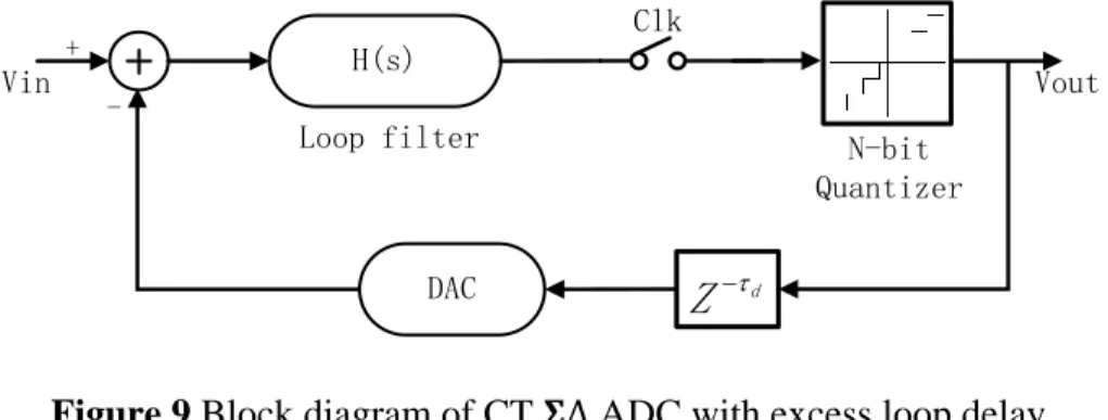
There is a finite amount of delay between the quantizer clock edge and the time when a change in output bit is seen at the feedback point in CT sigma delta modulator. It is commonly referred to excess loop delay (ELD) [7]. Excess loop delay changes modulator transfer function characteristic and affects the stability and dynamic range performance.
Figure 9 shows the block diagram of CT sigma delta modulator with excess loop delay.
21
H(s)
DAC
Loop filter N-bit
Quantizer Vin Vout + -d
Z
ClkFigure 9 Block diagram of CT 𝚺∆ ADC with excess loop delay
Given quantizer and DAC has unity-gain, the gain from quantizer output to input of sample and hold is given by
𝐺𝑎𝑖𝑛𝑓𝑏_𝑙𝑜𝑜𝑝 = 𝐻(𝑠) ∗ 𝑍−𝜏𝑑 (2.14)
where excess loop delay is modeled as 𝑍−𝑡𝑑 block and its absolute time domain value td=
𝜏𝑑𝑇𝑠. 𝑇𝑠 is sampling cycle. Excess loop delay changes equivalent z domain loop transfer
function [16] and has potential to cause instability. Given a constant td, increasing sampling frequency gives rise to larger 𝜏𝑑 and worse phase margin of loop gain. Thus excess loop delay limits the bandwidth of CT sigma delta modulator. Moreover [7] demonstrates that once excess loop delay exceeds a certain value for a certain loop structure it would raise in-band noise thus degrade SNR performance.
22 CHAPTER III
DESIGN OF CONTINUOUS-TIME SIGMA-DELTA MODULATOR
This chapter describes the system-level design of loop filter for 11-bit resolution 15MHz signal bandwidth continuous-time low-pass sigma-delta ADC. An important system-level consideration that can improve the overall power consumption is demonstrated along with the proposed modulator architecture. An overview of the implementation of system is presented.
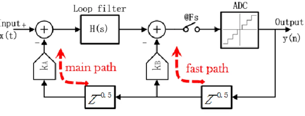
Background
[3] proposes local feedback technique to solve the problem of excess loop delay. The local feedback technique is also used in this thesis. Figure 10 shows the architecture in [3].
23
The sigma delta loop in Figure 10 has a local feedback path from output of the quantizer to input of S/H. This path is of low gain but has wide bandwidth. Thus it is also called fast path. The fast path is modeled as constant gain path in Figure 10. The main path is the one that feeds quantizer output to input of modulator. Note that a summing amplifier is needed to sum the output of loop filter and local feedback path.
For the case of NRZ DAC pulse, the whole loop gain of sigma delta modulator in z domain is obtained below by applying impulse invariant transform [16]
𝐻𝑙𝑔(𝑧) = 𝐻𝑚𝑝(𝑧) + 𝐻𝑓𝑝(𝑧) = (𝑘𝐴 ∗ 𝐻𝑙𝑓(𝑧) + 𝑘𝐵)𝑧−1 (3.1)
where 𝑘𝐵 and 𝑘𝐴 are the gain for feedback path DAC_A and DAC_B, respectively. 𝐻𝑙𝑓(𝑧) is the z domain loop filter transfer function. Equation (3.1) shows that local
feedback technique adds a DC path in parallel with 𝐻𝑙𝑓(𝑧). This path creates a zero thus compensates the phase shift of excess loop delay. From the point view of impulse response, fast path feeds quantizer output back into S/H promptly to maintain the equivalence between CT modulator and its DT counterpart even though excess loop delay exits.
An extra benefit of local feedback technique is the potential to reduce bandwidth requirement of opamp in loop filter. [11] points out that the influence of finite GBW in CT sigma delta modulator can be modeled as integrator gain-error and excess loop delay. Excess loop delay can be solved by the technique mentioned above. Coefficient tuning can fix integrator gain-error. In sum, in terms of transfer function error the bandwidth of filter opamp has no need to be very large as long as local feedback technique is used.
24
System Level Design Considerations
The architecture of the continuous-time sigma-delta modulator mainly determines its performance. Important architecture level choices include loop filter order, sampling frequency and number of quantizer bit. For an ideal sigma-delta modulator, the dynamic range of sigma delta modulator with Lth order noise transfer function equal to (1 − z−1)L
is
DR(in dB) = 10 ∗ lg [3 2
(2𝐿 + 1)𝑂𝑆𝑅2𝐿+1
𝜋2𝐿 ] + 6.02 ∗ (𝑁 − 1) (3.2)
where OSR is the oversampling ratio, L is the order of modulator order. N represents the number of bits in quantizer.
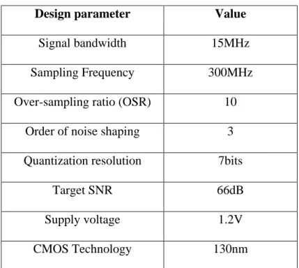
Higher order sigma-delta modulators are more suitable for wide bandwidth, high-resolution applications because they relax the over-sampling requirements given DR is constant. Multi-bit implementation of the quantizer increases the SNR by 6dB per quantizer bit, but it may suffer from mismatches in the feed-back DAC. In this work, a 3rd order, 7bit quantizer architecture with an OSR of 10 is chosen to implement a 15MHz bandwidth, 11-bit resolution continuous-time low-pass sigma-delta ADC.
Sigma-delta Loop Transfer Function
In this thesis, the quantizer is clocked by CLK and a D latch clocked by CLKB which is half cycle delay to CLK is added in between quantizer output and NRZ DAC. Thus excess loop delay is modeled as half sampling cycle. Local feedback technique is
25
used here. Main path delay is also set to be half sampling cycle. Our simplified system-level model is shown in Figure 11.
Figure 11 System-level model of our CT sigma delta modulator
The z domain loop gain transfer function of Figure 11 is given by
𝐻𝑙𝑔(𝑧) = 𝐻𝑚𝑝(𝑧) + 𝐻𝑓𝑝(𝑧) = 𝐻𝑚𝑝(𝑧) + 𝑘𝐵∗ 𝑧−1 (3.2)
where 𝐻𝑚𝑝(𝑧) is z domain main path transfer function.
An optimized NTF is chosen for 15MHz in-band quantization noise in z domain. Based on that, a loop transfer function Hloop(𝑧) is derived:
Hloop(𝑧) =1 − 𝑁𝑇𝐹(𝑧) 𝑁𝑇𝐹(𝑧) =
z3 − 1.424𝑧2+ 0.66𝑧 − 0.08931
𝑧4− 2.794𝑧3+ 2.691𝑧2− 0.8961𝑧 (3.3)
Then s-domain transfer function of sigma delta loop is obtained from impulse invariant transformation (IIT). The 3rd order loop filter transfer function is given by,
𝐻𝑙𝑝(𝑠) =3.416𝑒8𝑠2+ 5.394𝑒16𝑠 + 4.226𝑒24
𝑠3+ 3.291𝑒7𝑠2+ 9.746𝑒15𝑠 (3.4)
Loop filter ADC
x(t) y(n) + -@Fs H(s) k A kB 5 . 0
Z
-Input Output26
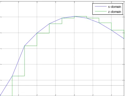
Local feedback path gain, kB, is 1. Figure 12 shows the impulse response interpolation of main path both in s domain and z domain at sampling times.
Figure 12 Impulse response of main path in s domain and z domain
Modulator Loop Topology
The loop filter of single stage sigma delta modulators are commonly implemented in two ways. One is chain of integrator with distributed feed-back (CIFB) and the other is chain of integrators with feed-forward summation (CIFF). Regarding circuit implementation CIFB topology requires multiple DACs feeding back to the input of each
0 0.5 1 1.5 2 2.5 3 x 10⁻⁸ 0 0.5 1 1.5 2 2.5 3 Impulse Response Time (seconds) Im p u ls e R e s p o n s e s-domain z-domain
27
integrator stage. Instead, CIFF topology with local feedback technique demands two DAC and an additional summing stage to perform feed-forward summation of integrator output. One important advantage CIFF offers over CIFB is restively small signal swing. The signal swing at the internal nodes of the modulator is relaxed in the case of feed-forward architecture with the help of coefficient scaling [8]. This is critical since larger signal swing demands opamp of better linearity. If the signal swing is too large, opamp might be forced to work in nonlinear region which results in lower opamp gain and increased distortion. Therefore the selection of modulator loop topology greatly affects the circuit implementation. A feed-forward topology is selected for our project.
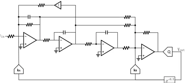
Proposed Modulator Architecture
With conventional feed-forward architecture, a 3rd order low pass CT Σ∆ ADC to implement the loop gain of equation (3.4) is shown in Figure 13. The feed-forward path consists a two-stage biqual filter, one active RC opamp, active summing amplifier and a quantizer.
28 -1 Vout Q 5 . 0 z kA kB Vin
Figure 13 A 3rd order CT Low pass 𝚺∆ ADC with feed-forward architecture
Such structure demands four opamps without regard to quantizer. Three of them are used as integrators in loop filter. The realization of local feedback path would require a summing amplifier. This solution introduces additional loop delay and also is power-hungry [3] [4] [17]
To avoid this, a differentiation operation is introduced in the local feedback path which allows the signal to be fed to the input of the last integrator. A new local feedback path is proposed. It consists of a continuous time differentiator and integrator. The integrator is provided by the active RC amplifier of loop filter’s last stage. In this way summing amplifier is removed. Correspondingly the summing node is moved forward to the last stage of loop filter. The summing operation of feed-forward paths are realized through capacitors. Figure 14 illustrates the development on the architecture of sigma delta modulator.
29 -1 Vin Vout Q 5 . 0 z kA S*Csa -1 N1 N2 -1 kB
Figure 14 Proposed CT sigma delta ADC architecture
The proposed 3rd order CT sigma delta ADC now only needs three opamps before quantizer. The system level design parameters for low-pass Σ∆ ADC are presented in Table 1
30
Table 1 System level design parameters for low-pass 𝚺∆ ADC
Design parameter Value
Signal bandwidth 15MHz
Sampling Frequency 300MHz
Over-sampling ratio (OSR) 10
Order of noise shaping 3
Quantization resolution 7bits
Target SNR 66dB
Supply voltage 1.2V
CMOS Technology 130nm
Note, the quantizer has 7-bit resolution but only 3 bits are applied to the sigma delta loop. The simple 3bit sigma delta modulator loop targets at 52dB SNR. The rest 4 bits of quantizer are used for calibration algorithm to boost the overall SNR to more than 66dB. The calibration algorithm is beyond the discussion of this thesis.
31 CHAPTER IV
DESIGN OF 3RD ORDER LOW-PASS LOOP FILTER
This chapter focuses on the design of 3rd order low-pass filter for a continuous-time Σ∆ ADC. Firstly, the structure and design equations of active RC integrator and biquadratic filter are reviewed. Secondly, design considerations for integrator are listed to guide design procedure. Finally a new linear class AB amplifier used to implement integrator is presented.
Background
A major challenge in the implementation of a low pass CT Σ∆ ADC with 15MHz and 11-bit ENOB is the design of loop filter. The dynamic range of loop filter must be better than the modulator specification.
Conventionally, the loop filter of CT Σ∆ modulator is realized with active integrator, such as active-RC or Gm-C integrator. Active-RC integrators provide better linearity (given highly linear resistors are available) at high frequencies and more insensitive to parasitic cap than their Gm-C counterparts, but consumes more power [8]. Furthermore, due to PVT variation RC time-constant in active-RC integrator is likely to change by ±20%. Thus a tuning circuitry is required.
The main non-ideality of active-RC integrators are due to finite trans-conductance (gm) and finite gain-bandwidth product (GBW) of amplifier. They alter the transfer function of loop filter, and potentially degrade overall performance of sigma delta ADCs.
32
Also circuit noise and distortion of integrator impacts the modulator performance. In contrast to error of subsequent stages, the one of first integrator are not subject to noise shaping within the sigma-delta loop. Thus, the first integrator limits the noise and linearity of entire loop filter.
Active RC Integrator
The structure of active RC integrator is shown in Figure 15.
C
R
V
inV
outA(s)
Figure 15 Active RC integrator
Ideally the transfer function of an active RC integrator is given by Vout(𝑠)
𝑉𝑖𝑛(𝑠) = −
1
𝑠𝑅𝐶 (4.1) Assume opamp is a first-order pole system defined by A(s). The transfer function of active RC integrator becomes
H(s) = − 1 sRC
𝐴(𝑠)
33
[8] points out that in the case of single-loop Σ∆ the DC gain of incorporated amplifier should be in the range of oversampling ratio Adc ≈ 𝑂𝑆𝑅 of the modulator. This requirement keeps every part of the in-band noise close to ideal noise shaping suppression. OSR in our project is 10 which is easy to fulfill. Here only finite GBW effect is included in our opamp model which is given by
A(s) =GB
𝑠 (4.3) Now integrator transfer function is
H(s) = − 1 sRC
𝐺𝐵
(𝐺𝐵 + 1𝑅𝐶) + 𝑠 (4.4)
GBW introduces integrator gain error for low frequencies and phase delay for high frequencies. [11] proposes that the effect of a finite GBW can be modeled as a corresponding integrator gain-error and feedback loop delays.
The integrator time constant can vary due to PVT variations of absolute values of resistor and capacitor. A switch capacitor band is used to compensate it as shown in Figure 16 Three control bits (b2, b1, b0) can provide ±20% tuning range. The switches are implemented with transmission gate with PMOS twice wider than NMOS. On one hand large W/L ratio is desired since ON resistance is inversely proportional to W/L of the transistor. On the other hand the parasitic increases if the switch size is increased. Therefore a nominal aspect ratio of W/L=80um/130nm was chosen in this design.
34
R
V
inV
out 0.8C 0.066C 0.132C 0.264C b0 b1 b2Figure 16 Capacitor tuning mechanism for integrator
Biquadratic Filter
A biquadratic filter is a two-integrator loop configuration as shown in Figure 17. It provides a band-pass node and a low-pass node.
-1 Vin
V
bp Vlp R2 R1 C C R4 R335
Ideally the transfer function of these two nodes are given by
HBP(𝑠) = − 1 𝑅3𝐶1𝑠 𝑠2+ 1 𝑅1𝐶1𝑠 +𝐶1𝐶21𝑅2𝑅4 (4.5) HLP(𝑠) = 1 𝐶1𝐶2𝑅3𝑅4 𝑠2+ 1 𝑅1𝐶1𝑠 +𝐶1𝐶21𝑅2𝑅4 (4.6)
Therefore, the design equations can be obtained, 𝜔02 = 1 𝑅2𝑅4𝐶1𝐶2 (4.7) Q = R1 √𝑅2𝑅4 √𝐶1 𝐶2 (4.8) A0 =𝑅2 𝑅3 (4.9) where A0 is the DC gain, ω0 is the cut-off frequency, and Q is the quality factor of the biquad.
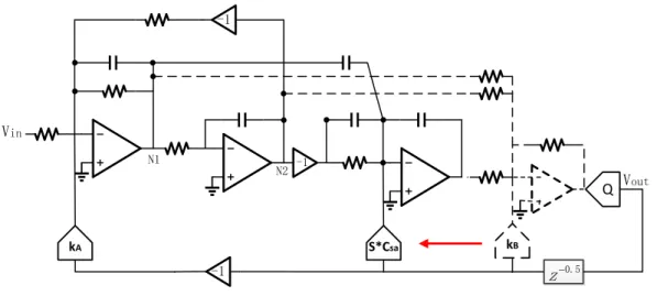
Loop Filter Architecture
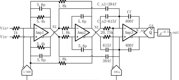
The 3rd order transfer function of the loop filter is realized using feed-forward architecture shown in Figure 18. All signal paths are fully differential. It consists of a two stage biquad filter and an active RC integrator. Opamp Amp3 provides a virtual ground at its inputs and helps summing node perform weighted addition of integrator outputs N1 and N2. The feed-forward coefficients are determined by the capacitor ratio, C_n1/Cf and
36
C_n2/Cf. The 3rd integrator also performs weighted addition of the local feedback path for compensating the excess loop delay.
Here, coefficient scaling is adopted to squeeze more gain to 1st stage. The way capacitors C_n1, C_n2 and Cf are determined will be discussed in the next chapter.
5 . 0 z Q 1k Vin+ Vin-5.6p 5.4k
Amp1 Amp2 Amp3
5.6p 5.6p 5.6p 5.4k 1/500 CLK S*Ca 615f 1.8k 1.8k 1.8k 20.75k C_n2=615f 400f 400f C_n1=384f 384f out N1 N1 N_sa Cf
Figure 18 3rd order loop filter
Opamp Design Considerations
GBW, Linearity and noise are three basic design considerations for opamps used in CT Σ∆ ADC. GBW is related to Σ∆ noise shaping effect. The latter two affect modulator dynamic range. All these parameters are ultimately attributed to opamp trans-conductance. In addition, slew rate and output swing are also important parameters which can be obtained from behavior model simulations. In this section opamp design focuses on how to determine an appropriate trans-conductance to fulfill specifications.
37
For single-loop architecture GBW = 2πfs is a reasonable limit without severe performance degradation [8], where fs is sampling frequency.
Regarding linearity analysis, we begin with the calculation of opamp loop gain. Figure 19 shows a general case of opamp working in a feedback loop.
A(s) Zf
Zin
V
inV
outFigure 19 Opamp in feedback
3rd harmonic (HD3) of opamp in feedback is given by [13] HD3loop =HD3OPAMP
[1 + 𝐿𝐺]3 (4.10)
The modulator targets at 11bit resolution. Give more margin in design and targeted SNR is set to 72dB. As is discussed in previous chapter the linearity of 1st integrator is critical. Any in-band error components occurring in this stage should be weaker than Psig/DR. DR is the dynamic range. Thus for 1st integrator the following equation should be satisfied
HD3loop > 72𝑑𝐵 (4.11) Given HD3OPAMP = 20𝑑𝐵, LG should be larger than 6 within 15MHz bandwidth based on equation (4.10).
38
The closed loop and open loop schematic of 1st integrator is shown in Figure 20. The opamp is modeled with trans-conductance in parallel with output resistor.
N1 Vin
(a) Closed loop
Gm
V
tV
fRL
CL
R1
C1
Rin
(b) Open loopFigure 20 Closed loop and open loop of 1st integrator
The loop gain is given by LG = 𝑅𝐿|| 1 𝑠𝐶𝐿||(𝑅𝑖𝑛+ 𝑅1|| 1 𝑠𝐶1) 𝑅𝑖𝑛 𝑅𝑖𝑛 + 𝑅1|| 1𝑠𝐶 1 (4.12)
39
Based on components value in Figure 20 and applying LG=6 @15MHz, we can calculate the desired Gm. With some margin, Gm for 1st integrator is found to be 10mS. Regarding 2nd and 3rd integrator the requirement on linearity is reduced considerably. Thus Gm for 2nd and 3rd opamp is scaled based on macro model calculation. Requirement of opamps’ trans-conductance are presented in Table 2.
Table 2 Trans-conductance needed for each opamp in terms of linearity
Opamp NO. Trans-conductance
1 10mS
2 5mS
3 5mS
When we calculate the local loop gain of 3rd opamp, the load from differentiator is neglected because differentiator output impedance is very large. Design issue of differentiator would be covered in next chapter.
In terms of noise, the total filter input-referred noise must be 72dB lower than signal power. Besides thermal noise from resistor, transistor also add noise. We will come back to noise analysis after we present our amplifier schematic.
40
A Linear Class AB Amplifier
In a low voltage design, usually two kinds of opamp architectures are popular, folded-cascode and two-stage. However, in a CT loop filter composed of the active RC integrators, the resistive load makes the folded-cascode opamp less efficient in terms of the DC gain than the two-stage opamp. Thus, in our design, all stages employ the latter one. All opamps should be biased such that they are never saturated during normal operation. In addition, during the start-up it is conceivable that the DAC is tipped all the way to one side while the input is tipped all the way to the wrong side, so the opamp should be able to handle large slew current without saturation. In order to save power, a class-AB output stage may be used to provide such a big output current with much lower biasing current. A conventional class-AB output stage which has excellent properties is shown in Figure 21 [18] [19].
Figure 21 Large output swing class-AB CMOS output stage with CM transistor coupling
41
The input can be added though either input ports, Vin1 or Vin2. The quiescent current of output stage is Iq. When a positive input voltage is added through Vin1 point, the current through M4 will increase by the same amount as the decrease of the current through M3, which makes the voltages at the gates of the output transistors increase the same amount. Ipull becomes larger while Ipush becomes smaller. This procedure will continue until all IB1(IB1= IB2) current flows though M4 and M3 is cut off, at which point Ipush = (2 − √2)2Iq and Ipull = 4Iq. After that, Ipush will keep the same minimal value while the Ipull can further increase far above 4Iq. In this way output stage can sustain a
large transient current with small quiescent current. A complete two-stage opamp with the above class-AB output stage is shown in Figure 22 [20]
Figure 22 Two-stage opamp with class AB output
Regarding small signal analysis of Figure 21, the small variation from one input port would be copied to the other one theoretically by setting gm,M3 = gm,M4. Body effect,
42
however, make this unity transfer gain changeable during transient state. Considering body effect the transfer gain from Vin1 to Vin2 is (gm3+ gmb3)/(gm4+ gmb4). gmb does not change linearly when signal varies thus conventional class AB output stage introduce distortions during transient state.
To overcome this problem, a linear class AB output stage is proposed as shown in Figure 23. AC signal from Vin1 can be coupled to Vin2 by large capacitor C2. Resistor R2 and DC current source I1 and I2 from common mode feedback circuit (CMFB) set the DC voltage for Vin2. The RC tank, R2 and C2 make the transfer gain from Vin1 to Vin2 independent with input signal transient state.
M3
M4
R2
C2
Vout
Vin1
Vin2
I1
I2
Figure 23 Proposed class AB output stage
The schematic of whole amplifier employing proposed linear class AB output stage is shown in Figure 24.
43 Vin+ M1 M1 Vin-M2 M2 R1 R1 M3 M4 C2 A C Von 200uA I1 I2 Vb R2 M3 M4 C2 B D Vop I1 I2 R2
Figure 24 Schematic of linear class AB amplifier
The 1st stage is a differential pair loaded with PMOS M2 and resistor R1, and directly drives M4 of 2nd stage. 1st stage trans-conductance output impedance is given by Rout1= 𝑟𝑜_𝑚2||𝑅1 (4.13)
where 𝑟𝑜_𝑚2 is transistor output impedance.
Current source I1 and I2 models the current branch in CMFB which will be discussed soon. I1 and I2 along with R2 provide a DC shift from node C to node A. C2 is a bypass capacitor through which AC signal from 1st stage is coupled to M3. At high frequency C2 provides a short path from node C to node A. Thus output stage consisting of M3 and M4 can perform class AB operation.
The design procedure of this linear class AB amplifier starts from 2nd stage. Based on macro model simulation result largest transient output current Imax is obtained. Quiescent current of class AB stage is set to be 1/3 Imax. Configure gm/id and Vdsat to be 20 and 90mV. Thus gm2 is known
44
For 1st stage, total input referred noise should be 72dB lower than signal power as we discussed in last section. That is,
2 (8 3 kT gm1+ 8 3 kTgm2 𝑔𝑚12 + 4kT 1 R1𝑔𝑚12 ) ∗ BW < −72dB (4.14)
Based on this equation, gm1 is obtained.
Amplifier equivalent trans-conductance GM is given by
Gm = 𝐴𝑣,1∗ 𝑔𝑚,2 (4.15) Thus R1 is also known.
Since amplifiers work in fully differential mode, common mode feedback circuit is indispensable. Figure 25 shows CMFB schematic. Two resistors are used to sense the common mode voltage of the opamp outputs, Vop and Von. An error amplifier is employed
to compare the common-mode voltage with reference voltage and feed a difference current to node A&B, as shown in Figure 24. Capacitor Ccs and Cmp are added for frequency compensation. Vref A B Vop Von Vmid Vmid 1 : 2 M5 M6 M7 M8 : 2 D Cmp Ccs Vb
45
Simulation Results
The 3rd order loop filter is designed and implemented in IBM 130nm technology. Figure 26 shows the layout view of loop filter.
46
(a) Squared input referred noise
(b) Noise summary
Figure 27 Noise performance of 1st opamp
As shown from Figure 27, input referred noise power is -92.9dB below full scale (1.2V)
47
Figure 28 Loop gain of 1st opamp
The simulation result for loop gain of 1st opamp is shown in Figure 28. The phase
margin is 61° at unite gain frequency of 900MHz. Loop gain is 6.84 (16dB) at 15MHz. Figure 29~31 demonstrate that proposed class AB amplifier achieves a better linearity than conventional one. Figure 30 describes opamps’ closed loop linearity regarding IM3. Figure 31 shows the IIP3 of amplifiers working. In the case of IIP3, the larger the value, the better linearity it indicates. Regarding HD3, the smaller the value, the better linearity it indicates. Table 3 summarizes two linearity tests.
48
Figure 29 Linearity test schematic
Figure 30 IM3 for conventional and proposed class AB amplifier
V
in+V
in-Vout
+Vout-C
1C
1C
1C
149
Figure 31 IPN curve for conventional and proposed class AB amplifier
Table 3 Summary of linearity performance
Conventional Proposed
Closed loop IM3 -67.52dB -83.16dB
50 (a) AC response
(b) Transient response
Figure 32 CMFB simulation result
Figure 32 proves that common mode loop of designed 1st stage opamp is stable. Figure 32(a) shows that common mode loop has a phase margin of 66.6° with a UGF=178.9MHz. Figure 32(b) shows that given two test currents of step waveform
51
injected at the outputs, the common mode output voltages could settle within a small period.
Figure 33 AC response of biquad filter
Top and bottom plot in Figure 33 represents bandpass and lowpass node of biquad filter, respectively.
52
(a) Squared input referred noise
(b) Noise summary
Figure 34 Noise performance of 3rd loop filter
Figure 34 shows the input-referred noise density and input-referred integrated noise of 3rd loop filter. Input referred noise power is -73.1dB below full scale (1.2V)
53 CHAPTER V
CONTINUOUS-TIME DIFFERENTIATOR
In this chapter problems with conventional differentiator implementation are analyzed and identified. A new differentiator that works in continuous time is proposed. Mathematical derivation and simulation of whole sigma delta loop are performed to prove that proposed differentiator is robust and surpass conventional implementation in terms of stability issue.
Discrete-time Differentiator
Conventional differentiator used in CT Σ∆ ADC is implemented in a discrete-time method as shown in Figure 35. A latch controlled by CLK provides an additional half cycle delay to feedback signal through DAC3. The feedback signal of DAC2 and a delayed version that is output of DAC3 are subtracted at the input of integrator. In effect, local feedback DAC output is proportional to the derivative of the quantizer output [4]. A corresponding system-level model is showed in Figure 36.
54
Figure 35 Conventional differentiator used in CT 𝚺∆ ADC
Figure 36 System-level model of CT 𝚺∆ modulator with DT differentiator
The signal processing chain of the fast path in Figure 35 is given by Figure 37. Quantizer output is delayed by half sampling cycle and feed into DAC2 and DAC3. An integrator then integrates differentiator output. An equivalent fast path output waveform is shown at the bottom of Figure 37.
55
Figure 37 Signal chain of DT differentiator in cascade with integrator
Applying impulse invariant transform to the fast path in Figure 36, the transfer function in z domain is given by
𝐻𝑓𝑝′ (𝑧) = 0.5𝐾𝑧−1 (5.1)
As shown from equation (5.1) the effective DAC current is scaled by half. This is because half of them is canceled by each other before being injected into integrator. To maintain a fast path gain of 1, each DAC current should be double. The pulse response interpolation for fast path at sampling times is shown in Figure 38.
Note, pulse response in this thesis and impulse response from [7] [16] refers to the same signal processing. Here, pulse response refers to injecting DAC pulse as the input and obtaining a response at the output. References like [7] [16] use the terminology, impulse response, because they model DAC as a building block and apply an impulse to DAC input and trigger a pulse at DAC output.
0 Ts/2 1.5Ts K/s DAC2 0 Ts/2 Ts K/2 Input of quantizer ADC 0 Ts 2Ts DAC3 + -2Ts
56
Figure 38 Pulse response interpolation of DT differentiator in cascade with integrator (sampling cycle is normalized to 1)
In integrated circuit, there are parasitic resistor and capacitor on the wire line that connects one node to another. These parasitic resistor and capacitor will introduce delay on the signal path. Moreover, PVT variation would lead to delay variation. In recent research work [5] [6] to achieve better dynamic performance, sampling frequency are pushed into GHz range leading to extremely small sampling cycle. Thus, the variation on excess loop delay cannot be neglected. Given variation on excess loop delay (ELD), DAC waveforms in the fast path would be like Figure 39. Here ϵ1 and ϵ2 models delay variation on DAC2 and DAC3, respectively.
0 1 2 3 4 5 6 7 8 9 10 0 0.1 0.2 0.3 0.4 0.5 0.6 0.7 0.8 0.9 1
Fast Path Pulse Response Interpolation at Sampling Times
Time (seconds) P u ls e R e s p o n s e s-domain z-domain
57
Figure 39 Equivalent fast path output waveform with ELD variation
The equivalent Z domain transfer function of fast path with ELD variation is given by
𝐻𝑓𝑝′ (𝑧) = 0.5𝐾𝑧−1+−𝜖1𝑧−1+ (𝜖1+ 𝜖2)𝑧−2− 𝜖2𝑧−3
1 − 𝑧−1 𝐾 (5.2)
ELD variation not only changes the fast path output value at the 1st following sampling time, but also affects the value at the 2nd following sampling time. This observation is shown in Figure 40.
0 K/s DAC2 0 Ts K(e2-e1) 0 DAC3
+
-2Ts 1 Ts/2 1.5Ts 1 Ts 2Ts 2 2 Ts/2 1 2 3Ts K(0.5+e2-e1)Input of
quantizer
ADC
58
Figure 40 Pulse response interpolation of DT differentiator in cascade with integrator given 10% ELD variation (sampling cycle is normalized to 1)
ELD variation causes severe problems on loop stability. As shown in Figure 40 10% ELD variation would cause 20% fast path output error at the next two sampling times. This is expected because effective DAC current is scaled by half after DT differentiator. Moreover, even larger ELD variation might make fast path lose its original role. That is, fast path might not be able to compensate ELD and keep sigma delta loop stable. Figure 41 shows the root locus of sigma delta closed loop transfer function with DT differentiator. It is easy to find that ELD variation cause pole movement, and that 25% ELD variation can push pole jump outside of unite cycle and make the loop unstable.
0 1 2 3 4 5 6 7 8 9 10 -0.1 0 0.1 0.2 0.3 0.4 0.5 0.6 0.7 0.8
Fast Path Pulse Response Interpolation at Sampling Times
Time (seconds) P u ls e R e s p o n s e s-domain z-domain
59 Pole-Zero Map Real Axis Im a g in a ry A x is -1 -0.8 -0.6 -0.4 -0.2 0 0.2 0.4 0.6 0.8 1 -1 -0.8 -0.6 -0.4 -0.2 0 0.2 0.4 0.6 0.8 1
Figure 41 Root locus of NTF vs ELD variation for DT differentiator
Continuous-time Differentiator
In sum, DT differentiator is sensitive to ELD. To overcome this shortcoming, a continuous time differentiator is proposed in the fast path as shown in Figure 42.
60 Vin-C1 Io+ Io-Io+ Io-Cf Cf Vin+ Vout-Vout+ Vcm_d Idac Vcm_d R0 M1 R0 M2 V1+ Figure 42 Proposed differentiator in cascade of integrator
Feedback DAC current Idac, is converted to voltage on one terminal of resistor 𝑅0 and then feed to differential pair M1 and M2 which work as source follower. Input signal is differentiated on capacitor C1, converted to current and forced to flow through transistor to the output of differentiator. Capacitor Cf along with an opamp integrates the output current of differentiator and generates a voltage signal at opamp output.
Transfer function of CT differentiator in cascade with an integrator is described by
𝐻𝑓𝑝(𝑠) =𝑉𝑜𝑢𝑡(𝑠) Vin(𝑠) = 𝑘′ 1 + 𝑠(2𝐶1)𝑟𝑜 1 + 𝑠 2𝐶1 𝑔𝑚 1 𝑠𝑟𝑜𝐶𝑓 = 𝑘′ 2𝐶1 𝐶𝑓 + 𝑘′ 𝑠𝑟𝑜𝐶𝑓− 𝑘′2𝐶1 𝐶𝑓 𝑔𝑚1𝑟𝑜 1 + 𝑠 2𝐶1 𝑔𝑚 (5.3)
where 𝑘′= 𝐼𝑑𝑎𝑐∗ 𝑅0, 𝑔𝑚 is the trans-conductance of M1 and M2 and 𝑟0 is transistor
output impedance. Now the structure of designed Σ∆ modulator evolves into what Figure 43 shows
61
Figure 43 Block diagram of CT 𝚺∆ modulator with CT differentiator
Given 𝑔𝑚𝑟𝑜 is very large, the above fast path gain can be simplified as 𝐻𝑓𝑝(𝑠) ≈ 𝑘′
2𝐶1 𝐶𝑓 +
𝑘′
𝑠𝑟𝑜𝐶𝑓 (5.4)
Apply impulse invariant transform to equation (5.4). The z domain transfer function for fast path is obtained
𝐻𝑓𝑝(z) = 𝑘′( 2𝐶1 𝐶𝑓 + Ts 2roCf) z −1+ 𝑘′ Ts roCf z−2 1 − 𝑧−1 (5.5)
Pulse response interpolation of CT differentiator in cascade with integrator is shown in Figure 44.
Loop filter ADC
x(t) y(n) + -@Fs H(s)
k
A 5 . 0 Z
-Input OutputH
fp(s)
Vin-C1 Io+ Io-Io+ Io-Cf Cf Vin+ Vout-Vout+ Vcm_d Idac Vcm_d R0 M1 R0 M2 V1+V1-62
Figure 44 Pulse response interpolation of CT differentiator in cascade with integrator (sampling cycle is normalized to 1)
Given ELD variation, DAC waveforms in the proposed fast path would be like Figure 45. Here 𝜖 models delay variation on feedback DAC.
Figure 45 ELD variation in proposed fast path DAC
0 1 2 3 4 5 6 7 8 9 10 0 0.2 0.4 0.6 0.8 1 1.2 1.4
Pulse Response Interpolation at Sampling Times
Time (seconds) P u ls e R e s p o n s e s-domain z-domain 0