UC Davis Previously Published Works
Title
High-Order Dual-Port Quasi-Absorptive Microstrip Coupled-Line Bandpass Filters
Permalink
https://escholarship.org/uc/item/9g39v39h
Journal
IEEE Transactions on Microwave Theory and Techniques, PP(99)
ISSN
0018-9480
Authors
Wu, Xiaohu
Li, Yingsong
Liu, Xiaoguang
Publication Date
2019
DOI
10.1109/tmtt.2019.2955692
Peer reviewed
eScholarship.org
Powered by the California Digital Library
High-Order Dual-Port Quasi-Absorptive Microstrip
Coupled-Line Bandpass Filters
Xiaohu Wu,
Senior Member, IEEE,
Yingsong Li,
Senior Member, IEEE,
Xiaoguang Liu,
Senior Member, IEEE
Abstract—In this paper, we present the first demonstration of distributed and symmetrical all-band quasi-absorptive filters that can be designed to arbitrarily high orders. The proposed quasi-absorptive filter consists of a bandpass section (reflective-type coupled-line filter) and absorptive sections (a matched resistor in series with a shorted quarter-wavelength transmission line). Through detailed analysis, we show that the absorptive sections not only eliminate out-of-band reflections but also determine the passband bandwidth. As such, the bandpass section mainly determines the out-of-band roll-off and the order of the filter can be arbitrarily increased without affecting the filter bandwidth by cascading more bandpass sections. A set of
2.45-GHz 1-, 2-, and 3-pole quasi-absorptive microstrip bandpass filters are designed and measured. The filters show simultaneous input and output absorption across both the passband and the stopband. Measurement results agree very well with the simulation and validate the proposed design concept.
Index Terms—Absorptive filter, bandpass filter(BPF), coupled lines, microstrip filter.
I. INTRODUCTION
F
ILTERS are essential building blocks of nearly every modern RF/microwave system. Conventional microwave filters reject undesired signals in the stopband by presenting a reactive impedance, i.e. the filters are reflective in the stopband. In practice, the reflective nature of theses filters may present a system level problem when connected to non-linear circuits such as power amplifiers and mixers. In many cases, the performance of these non-linear circuits are sensitive to out-of-band impedances, particularly those at the harmonics. As such, the use of reflective filters may result in unpredicted system performance degradation such as loss of efficiency, excessive spurious signal levels, and loss of dynamic range [1], [2].Conventional solutions to this problem involve using attenuators or non-reciprocal components, such as isolators Manuscript received March 10, 2019; revised September 5, 2019; accepted November 17, 2019.
This work is supported by Projects Grant from the National Natural Science Foundations of China No. 61601234, the Natural Science Foundation of Jiangsu Province No. BK20160965, and in part by a fellowship from the Postdoctoral International Exchange Program of China Postdoctoral Science Foundation (CPSF). (Correspondence author: Xiaohu Wu.)
X. Wu is with the Collaborative Innovation Center on Forecast and Evaluation of Meteorological Disaters, Nanjing University of Information Science and Technology, Nanjing, China, and also with the Department of Electrical and Computer Engineering, University of California, Davis, 95618, USA. e-mail: xhwu@ieee.org
Y. Li is with the College of Information and Communication Engineering, Harbin Engineering University, Harbin, China. He was a visiting scholar with the University of California, Davis, 95618, USA. e-mail: liyingsong@ieee.org X. Liu is with the Department of Electrical and Computer Engineering, University of California, Davis, 95618, USA. e-mail: lxgliu@ucdavis.edu
and circulators, to reduce the reflections of undesired spurious signals, albeit at the obvious cost of significant signal loss, cost, size, and weight of the system. Recently, the concept of
“absorptive” or “reflectionless” filters has been proposed as a
viable alternative solution that promises lower overall system performance degradation [3]. In an absorptive filter, the port impedances are well matched both in-band and out-of-band. While the in-band signals pass through the filter with minimal insertion loss, the out-of-band signals are not reflected but attenuated inside the filter.
The idea of absorptive filters was first introduced in [4] as a “non-reflecting branching filter”. The filter consists of two hybrid junctions, two identical reflective-type bandpass filters (BPFs) tuned to the absorption band, and two quarter-wavelength waveguides. Later, traveling-wave directional filters are reported to achieve input-port reflectionless performance [5], [6]. The cascaded microstrip directional filters [7] and miniaturized half-mode substrate integrated waveguide directional filter [8] also achieve one-port quasi-absorptive responses. Here, we use
“quasi-absorptive” to indicate that the reflection from the
filter is not ideally zero but a practically small value. Because the two couplers are arranged in a loop in these filters, the overall circuits are bulky, bandwidth-limited, and only absorptive at their input port, viz., the output port is still fully reflective in the stopband.
Absorptive filters can also be realized by using the complementary-duplexer architecture consisting of a main and an auxiliary channel with opposite filtering transfer functions [9], [10]. Coupling-matrix based analysis reveals that by loading the auxiliary channel with the system impedance and taking the output node of the main channel as the output terminal of the overall circuit, a filtering network of the same type of the main channel can be realized with theoretically perfect input-reflectionless behavior at all frequencies.
Multiple identical single-stage circuits can be cascaded to improve the passband selectivity at the cost of multiplied circuit size and number of components. Duplexer-style one-port absorptive lowpass filters with arbitrary transfer functions are designed using complementary susceptance cancellation in [11]. The same idea is used to develop microstrip one-port absorptive multiband bandpass and bandstop filters [12], filtering power dividers [13], reconfigurable BPFs [14], and multiplexers [15]. To achieve two-port absorptive filtering responses, one more auxiliary channel can be loaded at the output port [16], [17].
Low-Q lossy resonators are also used to achieve either one-port absorption [18]–[20] or symmetrical two-port
1 2 N Bandpass Sections Absorptive stubs Absorptive stubs Port 1 Port 2
Fig. 1. Conceptual circuit diagram of aNth-order quasi-absorptive BPF using absorptive parallel-coupled feedlines.
absorption [21]–[25] for bandstop filters. Quasi-Gaussian lowpass filter prototypes are reported with both ports reflectionless because of the lossy components in the circuit [26], [27]. A3.0-GHz distributed quasi-absorptive BPF is presented in [28] by using resistor-loaded lossy resonators as its first resonator to absorb reflection at only one side.
Lumped-element symmetrical two-port absorptive filters are reported in [29]. The design is based on a symmetrical circuit whose even- and odd-mode circuits have equal amplitude reflection coefficients with opposite signs at all frequencies. As a result, the overall circuit is ideally reflectionless for all frequencies. The design results in a large number of circuit elements with tight tolerance requirements. In [30], the concept is extended to support any transfer function by applying proper circuit transformations. In addition, a distributed absorptive BPF is proposed by using Richard’s transformations and Kuroda’s identity in [31]. However, the distributed absorptive BPF is not reduced to practice due to the extreme transmission-line impedance and coupled lines coupling coefficient [31, Eq. 3].
In [32], symmetric quasi-absorptive microstrip BPFs are implemented based on complementary branch-line bandpass and bandstop filters. A direct in-series cascade of two identical 1-pole stages is proposed to enhance the stopband attenuation with doubled circuit size. Both simulation and measured results show quasi-absorptive behavior in a limited frequency range [32, Fig. 14 and Fig. 16]. Complementary 2-pole bandpass and bandstop structures are also presented, however, the size of the overall circuit is three times the main bandpass section as a result of the two auxiliary bandstop sections.
In this paper, a new quasi-absorptive BPF architecture is proposed and experimentally validated. Fig. 1 shows a conceptual circuit schematic of the proposed filter structure. Bandpass response is realized by parallel coupled lines sections similar to a conventional coupled-line filter. To achieve absorption at all frequencies, absorptive stubs each consisting of a series resistor and a shorted quarter-wavelength stub load the input and output of the coupled-line sections. At the center frequency, these stubs appear as open circuit. Outside of the passband, the stubs appear as matched load
(c) (a) (b) ZS R 2R 2R θ e , θo θ θ θ 2Z S 4' 1' 2' 3' Port 1 Port 2 4' 1' 2' 3' Port 1 Port 2 2Z S 4' 1' 2' 3' Zin2 S Z c1, k1 Z in1 S Zin2 D ZinD1
Fig. 2. Evolution of quasi-absorptive coupled-lines. (a) Conventional four-port coupled-lines. (b) One-port quasi-absorptive coupled-line with singly-loaded absorptive stub resistive loading. (c) One-port quasi-absorptive coupled-line with doubly-loaded absorptive stubs.
to the ground and contribute to the absorption of out-of-band signals. Compared with other state-of-the-art absorptive filters, particularly [31] and [32], the proposed architecture is the first that realizesa distributed and symmetrical all-band absorptive
filter that can be extended to arbitrarily high orders. We
validate the proposed concept by demonstrating a set of
2.45-GHz absorptive filters showing 1-, 2-, and 3-pole roll-off characteristics. In all cases, measurement results match very well with the simulation.
II. QUASI-ABSORPTIVECOUPLEDLINES
This section introduces the concept and design of quasi-absorptive coupled lines which forms the basis of the proposed quasi-absorptive filters.
Fig. 2 (a) shows a section of conventional parallel-coupled lines with the four ports labeled by 10, 20, 30, and 40. Zc1
and k1 are the coupled impedance and coupling coefficient,
respectively. The coupled lines have an even-mode impedance
Ze1 = Zc1k1 and an odd-mode impedance Zo1 = Zc1/k1.
θe and θo are the even- and odd-mode electrical length, respectively [33]. To simplify the model and the analysis,
θe = θo = 90◦ at the center frequency. For simplicity, Normalized frequency f /f0 is used in the circuit analysis,
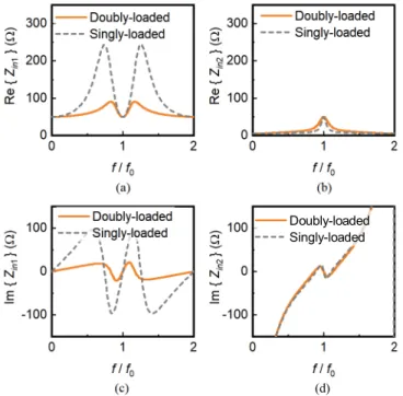
0 1 2 0 100 200 300 0 1 2 0 100 200 300 0 1 2 -200 0 200 0 1 2 -200 0 200 0 1 2 0 100 200 300 0 1 2 0 100 200 300 0 1 2 -200 0 200 0 1 2 -200 0 200 f / f 0 R e { Z S i n 1 } ( W ) (a) R = 35, 50, 65 W f / f 0 R e { Z S i n 2 } ( W ) (b) R = 35 W R = 50 W R = 65 W I m { Z S i n 1 } ( W ) f / f 0 (c) R = 35, 50, 65 W I m { Z S i n 2 } ( W ) f / f 0 (d) R = 35 W R = 50 W R = 65 W R e { Z S i n 1 } ( W ) f / f 0 (e) Z s = 10, 21.5, 33 W f / f 0 R e { Z S i n 2 } ( W ) Z s = 10 W Z s = 21.5 W Z s = 33 W (f) I m { Z S i n 1 } ( W ) f / f 0 (g) Z s = 10, 21.5, 33 W I m { Z S i n 2 } ( W ) f / f 0 Z s = 10 W Z s = 21.5 W Z s = 33 W (h)
Fig. 3. Input impedance analysis of singly-loaded coupled line with respect toRandZs(Zc1= 98 Ω,k1= 1.63, andZ01=Z02= 50Ω). (a)–(d) shows
the calculated frequency dependence of Re{ZS
in1}, Im{ZinS1}, Re{ZinS2}, and Im{ZSin2}, respectively, for variousRvalues (Zs= 21.5 Ω). (e)–(h) shows
the calculated frequency dependence of Re{ZS
in1}, Im{ZSin1}, Re{ZinS2}, and Im{ZinS2}, respectively, for variousZsvalues (R= 50 Ω).
The impedance matrix of the conventional four-port parallel-coupled line structure can be expressed as in [34]
V10 V20 V30 V40 = Z1010 Z1020 Z1030 Z1040 Z2010 Z2020 Z2030 Z2040 Z3010 Z3020 Z3030 Z3040 Z4010 Z4020 Z4030 Z4040 I10 I20 I30 I40 , (1) where Z1010 =Z2020 =Z3030 =Z4040 =−j Zc1 2 (k1+ 1 k1 ) cotθ, (2a) Z1020 =Z2010 =Z3040 =Z4030 =−j Zc1 2 (k1− 1 k1 ) cscθ, (2b) Z1030 =Z3010 =Z2040 =Z4020 =−j Zc1 2 (k1+ 1 k1 ) cscθ, (2c) Z1040 =Z4010 =Z2030 =Z3020 =−j Zc1 2 (k1− 1 k1 ) cotθ. (2d) Coupled-line sections with one or two ports terminated in open circuit, short circuit, or matched load are widely used as building blocks for reflective filters [35]. In such filters, signals in the stopband sees a reactive impedance and is fully reflected.
In this work, we propose quasi-absorptive coupled lines as building blocks for quasi-absorptive BPFs. Shown in Fig. 2 (b) and Fig. 2 (c), the coupled-line section is loaded with one or two resonant absorptive stubs.
In Fig. 2 (b), the absorptive stub consists of a resistor R
and a shorted stub with a characteristic impedance of Zs
and an electrical length ofθ. In Fig. 2 (c), the absorptive stub in Fig. 2 (b) is split into two identical absorptive stubs that load both ends of one of the coupled-lines. The following sub-sections analyze the characteristics of these two circuits.
A. Quasi-Absorptive Coupled Lines with a Single Absorptive Stub
In Fig. 2 (b), Port10 and Port20 act as the input and output ports of the circuit. Port40 is open-ended and Port30is loaded by an absorptive branch. Zin1 and Zin2 are defined as the
input impedance at Port 1 and Port 2, respectively.
Applying the boundary conditions I40 = 0 and V30 = −ZstubS I30 to (1), we have I30 I40 = − Z1030 Z1010 +ZstubS − Z1040 Z1010+ZstubS 0 0 I10 I20 , (3) whereZS
stub=R+jZstanθ. Substituting (3) into (1) yields the two-port impedance matrixZbwhose element values are
Z11S =Z1010− Z10302 Z1010+ZS stub , (4a) Z12S =Z21S =Z1020 − Z1040Z1030 Z1010 +ZS stub , (4b) Z22S =Z2020− Z10402 Z1010+ZS stub . (4c)
Doubly-loaded Singly-loaded
(d)
Fig. 4. Comparison between the calculated input impedance profiles of the singly-loaded [Fig. 2 (b)] and the doubly-loaded [Fig. 2 (c)] quasi-absorptive coupled lines (Zc1 = 98 Ω,Zs = 21.5 Ω,k1 = 1.63,R= 50 Ω,Z0 =
50 Ω). (a) Re{Zin1}. (b) Re{Zin2}. (c) Im{Zin1}. (d) Im{Zin2}.
The input impedance of a general two port network can be extracted from its Z-parameters as
Zin1=Z11− Z12Z21 Z22+Z0 , (5a) Zin2=Z22− Z12Z21 Z11+Z0 , (5b)
whereZ0is the port impedance and is set to50 Ωin this paper.
Taking (2) and (4) into (5) gives us the synthesized port impedanceZS
in1andZinS2for the single-absorptive-stub loaded
coupled-line. It is obvious that both ZS
in1 and ZinS2 are
frequency-dependent functions of the four design parameters
Zc1, k1, Zs, andR. Explicit expressions ofZinS1 andZ S in2 in
terms of the above parameters may be derived but are too complicated to give design insights, except at a few specific frequencies. For example, by setting θ =π/2 for the center frequencyf0in (2), (4), and (5), we have
ZinS1|f0 =ZinS2|f0 =Z
2
c1(k1−1/k1)2
4Z0
, (6)
which is the same as the conventional coupled-line circuit [33].At the same time,θ=nπ for the even harmonics
2nf0,(n= 0,1,2,· · ·), we have
ZinS1|2nf0=R, (7a)
ZinS2|2nf0=−j∞. (7b)
To better understand the characteristics of the absorptive coupled lines, we present in Fig. 3 a numerical study of the port input impedances in terms of the design parameters. Several observations can be made.
1) Unlike conventional coupled lines, Port 1 of the quasi-absorptive coupled lines can be impedance matched not only at f0 but also at dc and the even harmonics.
From (6) and (7), we can see that a perfect match can be achieved at any multiples off0 by the proper choice
of Zc1, k1, and R [Fig. 3 (a) and Fig. 3 (c)]. On the
other hand, Port 2 of the quasi-absorptive coupled lines is matched only at the odd multiples off0.
2) The maximum mismatch of Port 1 is highly dependent on
R[Fig. 3 (a) and Fig. 3 (c)] and relatively independent of
Zs[Fig. 3 (e) and Fig. 3 (g)]. A largerRleads to a lower maximum mismatch at the penalty of a higher mismatch at the even harmonics. The choice ofR is dependent on the application. In some applications, e.g., after a strong nonlinear amplifier, it may be desirable to have high absorptive performance at the even harmonics, therefore mandating R = Z0. ZinS2 is almost entirely determined
by the coupled lines and independent of the absorptive stub (R andZs).
We note that the absolute maximum mismatch for the singly-loaded quasi-absorptive coupled lines is still quite high, a problem that we seek to solve in the next sub-section.
3) The matching bandwidth of Port 1 around f0 is almost
independent ofR but is a strong function ofZs. Shown in Fig. 3 (e) and Fig. 3 (g),Zsaffects the rate of change of both the real and imaginary parts ofZinS1 atf0. As will
be shown in Section III, this property is used to control the passband bandwidth of the absorptive filters presented in this work.
4) Intuitively, the different matching characteristics of Port 1 and Port 2 may be understood by observing that the absorptive stub is connected with Port 1 through a quarter-wavelength transmission line, such that the input resistance and reactance at Port 1 vary in a relative smaller range when compared with these at Port 2.
B. Quasi-Absorptive Coupled Lines With Two Absorptive Stubs
To improve the absorption performance across all bandwidth, the single absorptive stub can be split into two identical stubs that load both ends of the coupled lines, as shown in Fig. 2 (c).
Following the same procedures in Section II-A, the impedance matrix ZD for doubly-loaded quasi-absorptive coupled lines can be derived
Z11D = Z D stubM M +ZD stub , (8a) Z12D =Z21D= Z D stubN M +ZD stub , (8b) Z22D =P− N 2 M +ZD stub , (8c)
Doubly-loaded Singly-loaded (c) | S 1 1 | & | S 2 2 | & | S 2 1 | d B f / f 0 |S 22 | |S 11 | |S 21 | (d)
Fig. 5. Comparisons of the singly-loaded [Fig. 2 (b)] and the doubly-loaded [Fig. 2 (c)] quasi-absorptive coupled lines in terms of calculated S-parameters (Zc1= 98 Ω, Zs= 21.5 Ω, k1= 1.63, R= 50 Ω, Z0= 50 Ω): (a)|S11|,
(b) |S22|, and (c) |S12|. (d) Wideband S-parameters of the doubly-loaded
quasi-absorptive coupled lines .
where
ZstubD = 2(R+jZstanθ), (9a)
M =Z1010− Z10302 Z1010+ZD stub , (9b) N =Z1020− Z1040Z1030 Z1010+ZD stub , (9c) P =Z2020− Z10402 Z1010+ZD stub . (9d)
The port input impedancesZinD1 andZinD2 can be obtained by taking (2), (8), and (9) into (5). The input impedances of doubly-loaded quasi-absorptive coupled lines are found to be exactly the same with those of the singly-loaded circuit at any
multiples of f0, as given in (6) and (7). In other words, both
can be fully matched not only atf0 but also at any harmonic
frequencies.
Fig. 4 shows a comparative study of the impedance profiles of the singly- and doubly-loaded quasi-absorptive coupled lines while Fig. 5 compares theirS-parameters. Some observations can be made.
1) It can be seen from Fig. 4 (a) that Port 1 of the doubly-loaded circuit has a much smaller impedance variation (real part of 50 Ω to 89 Ω and imaginary part of −21 Ω to 21 Ω) than that of the singly-load circuit (real part of50 Ωto245 Ωand imaginary part of−100 Ω
to +100 Ω). This leads to a much reduced reflection, i.e., improved absorption, at Port 1 for all frequencies, as shown in Fig. 5 (a),
2) Similar to the singly-loaded quasi-absorptive coupled lines, Port 2 of the doubly-loaded circuit resembles the reflective characteristics of conventional coupled lines. Fig. 4 (b) shows that the Re{Zin2} of doubly-loaded
quasi-absorptive coupled lines has a slightly less rate of change than that of the singly-loaded quasi-absorptive coupled lines, contributing to a wider matching and transmission bandwidth aroundf0 as shown in Fig. 5 (b)
and Fig. 5 (c), respectively.
3) Unlike the distributed branch-line filters in [9] and [32], which are quasi-absorptive in a limited frequency range, the proposed quasi-absorptive coupled lines consist of quarter-wavelength transmission lines and have periodic frequency responses [33]. Fig. 5 (d) shows that all-band quasi-absorptive can be obtained at Port 1 with spectral period of [0,2f0). The spurious passband occurs at the
odd harmonic frequencies and the stopband at the even harmonic frequencies are all suppressed by the periodic transmission zeros of the coupled lines [35]. This unique all-band quasi-absorptive property of the doubly-loaded coupled-lines will be used in the design of distributed all-band quasi-absorptive BPFs in Section III.
4) Another benefit of splitting the absorptive stub that may not be immediately obvious is that it allows easier microstrip implementation. As will be detailed in Section. III-A, the optimized value ofZs(Zs= 21.5 Ω) is too low for microstrip implementation. By splitting the absorptive stub into two identical sections, both R and
Zs double in value. A characteristic impedance of 43 Ω is much easier to realize.
III. QUASI-ABSORPTIVEFILTERS
The proposed quasi-absorptive parallel-coupled lines will be applied to design quasi-absorptive BPFs in this section. First, basic 1-pole quasi-absorptive BPF is explored and detailed parametric studies are carried out to illustrate its unique performance and the optimization method. Subsequently, higher-order (e.g., 2-pole and 3-pole) topologies through the basic 1-pole quasi-absorptive BPF are presented and studied. Detailed design and optimization procedures are accordingly provided. Finally, a comparison between the reported distributed quasi-absorptive BPFs and this work is
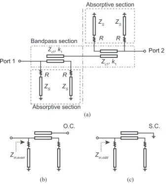
S.C. O.C. (a) (b) (c) Bandpass section ZS R ZS R R R Z S ZS Absorptive section Absorptive section Z c1, k1 Z in,even Zin,odd Zc1, k1 Port 1 Port 2
Fig. 6. (a) Transmission line circuit model of the 1-pole quasi-absorptive BPF . (b) Equivalent even-mode circuit with open-circuit (O.C.) termination. (c) Equivalent odd-mode circuit with short-circuit (S.C.) termination.
given to illustrate the advantages and disadvantages of the presented work.
A. 1-Pole Quasi-Absorptive BPFs
The doubly-loaded quasi-absorptive coupled lines presented in Section II-B are quasi-absorptive in only one of their two ports. By connecting two doubly-loaded quasi-absorptive coupled lines back-to-back, a symmetrical quasi-absorptive network can be created as shown in Fig. 6. Apparently, this circuit resembles a half-wavelength resonator coupled through quarter-wavelength coupled lines [labeled as “bandpass section” in Fig. 6 (a)]. The difference is the four absorptive stubs added to the input and output feedlines [labeled as “absorptive section” in Fig. 6 (b)].
We will analyze this 1-pole filter (coupled resonator) circuit to understand its characteristics and design trade-offs. Because the circuit is symmetric, it can be analyzed using the even-odd mode analysis. Fig. 6 (b) and Fig. 6 (c) show the even- and odd-mode circuit, respectively. The even- and odd-mode input impedance can be derived from two port impedance matrix as
Ze=Z11, (10a)
Zo=Z11−
Z12Z21
Z22
, (10b)
where Zij are the Z-parameters of the doubly-loaded quasi-absorptive coupled lines given in (8). From (10), the S-parameters of the 1-pole quasi-absorptive BPF can be readily derived.
For illustration purposes, S-parameters of an example 1-pole quasi-absorptive BPF are shown in Fig. 7. As a comparison, the S-parameters of the same circuit but without the absorptive
Bandpas s s ec tion Quas i-abs orptive BPF
Fig. 7. (a) Simulated |S21| of the 1-pole quasi-absorptive BPF and its
bandpass section. (b) Simulated |S11|of the 1-pole quasi-absorptive BPF
and its bandpass section.
stubs are also shown in Fig. 7. The 1-pole quasi-absorptive BPF shows quasi-absorptive responses with return loss better than 13 dB at all frequencies. Due to the presence of the absorptive stubs, the in-band transmission flatness is degraded. The absorptive stubs also lead to a much narrower passband in the 1-pole quasi-absorptive BPF when compared with its “bandpass section” only. This is generally true for other reported absorptive/reflectionless BPFs [9], [31], [32].
A few variables are labeled in Fig. 7 to facilitate a more detailed analysis later on. BW, Rs, and Rp are the 3-dB bandwidth of the passband, maximum stopband reflection, and maximum passband reflection, respectively. F BW is defined as the fractional 3-dB bandwidth, viz.,F BW =BW/f0. Five
reflection zeros can be observed in the range of dc–2.0GHz. Three of them, fp1, fp3, and fp5, are located at dc, f0, and
2f0, respectively. Another two reflection zeros (fp2 andfp4)
are symmetrically located aroundf0.
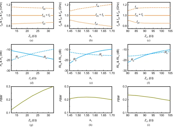
Although theoretical expressions for the transmission and reflection characteristics of the 1-pole quasi-absorptive BPF can be derived, they are too complicated to give design insights. Therefore, Fig. 8 presents parametric studies of the characteristics of the 1-pole quasi-absorptive BPF . Fig. 8 (a), Fig. 8 (b), and Fig. 8 (c) show the locations of the reflection zeros with respect to ZS,k1,Zc1, respectively. Fig. 8 (d)–(f)
and Fig. 8 (g)–(i) show the corresponding change in the reflection level and 3-dB bandwidth, respectively. In these figures, fp1 and fp5 are not shown because they are fixed
at dc and2f0.
When the transmission-line-stub impedance Zs increases from 12.5 Ω to 32.5 Ω, a large increase of F BW can be
15 20 25 30 0.8 1.0 1.2 15 20 25 30 -30 -20 -10 15 20 25 30 0.1 0.2 0.3 1.45 1.50 1.55 1.60 1.65 1.70 0.8 1.0 1.2 1.45 1.50 1.55 1.60 1.65 1.70 -30 -20 -10 1.45 1.50 1.55 1.60 1.65 1.70 0.1 0.2 0.3 80 85 90 95 100 105 0.8 1.0 1.2 80 85 90 95 100 105 -30 -20 -10 80 85 90 95 100 105 0.1 0.2 0.3 Z S (W ) f p 2 & f p 3 & f p 4 ( G H z ) f p4 f p3 = f 0 f p2 (a) Z S (W ) R p & R s ( d B ) R s R p (d) F B W Z S (W ) (g) k 1 f p 2 & f p 3 & f p 4 ( G H z ) f p2 f p3 = f 0 f p4 (b) R L p & R L s ( d B ) k 1 R p R s (e) F B W k 1 (h) Z c1 (W ) f p 2 & f p 3 & f p 4 ( G H z ) f p4 f p3 = f 0 f p2 (c) Z c1 (W ) R L p & R L s ( d B ) R s R p (f) F B W Z c1 (W ) (i)
Fig. 8. Parametric studies of the 1-pole quasi-absorptive BPF . (a) Reflection poles versusZs(k1= 1.55,Zc1= 92 Ω,R= 50 Ω). (b) Reflection poles
versus coupling coefficientk1 (Zs= 21.5 Ω,Zc1 = 92 Ω,R= 100 Ω). (c) Reflection poles versus coupling impedanceZc1 (Zs= 21.5 Ω,k1 = 1.55,
R= 50 Ω). (d) In-band reflectionRpand out-of-band reflectionRsversus stub impedanceZs(k1= 1.55,Zc1= 92 Ω,R= 50 Ω). (e) In-band reflection
Rpand out-of-band reflectionRsversus coupling coefficientk1(Zs= 21.5 Ω,Zc1= 92 Ω,R= 50 Ω). (f) In-band reflectionRpand out-of-band reflection Rs versus coupling impedanceZc1 (Zs = 21.5 Ω,k1= 1.55,R= 50 Ω). (g) FBW versus stub impedanceZs (k1 = 1.55,Zc1 = 92 Ω,R= 50 Ω).
(h) FBW versus coupling coefficientk1 (Zs = 21.5 Ω,Zc1 = 92 Ω,R= 50 Ω). (i) FBW versus coupling impedanceZc1 (Zs = 21.5 Ω,k1 = 1.55,
R= 50 Ω).
observed from 12% to 30% with deteriorated Rs. The two reflection zeros fp2 and fp4 move slightly closer to fp3,
resulting in an improvedRp.
As the coupling coefficientk1 increases from1.45to1.70,
fp2 and fp4 move away from f0, leading to an increased
Rp and decreased Rs. Interestingly, the bandwidth of the 1-pole quasi-absorptive BPF is almost independent of k1,
where as it is well known that the coupling coefficient k in the conventional coupled-line BPFs can be effectively used to control the filter bandwidth [35]. This is because the bandwidth of the 1-pole quasi-absorptive BPF is primarily determined by the absorptive stubs. In fact, this can be been in Fig. 7 (a). For the corresponding k1 values, the bandwidth
of the bandpass section [Fig. 6 (a)] is much wider than that of the 1-pole quasi-absorptive BPF itself.
F BW increases from 19% to23% asZc1 decreases from
105 Ωto80 Ωwith a corresponding improvement of bothRs and Rp. fp2, fp3, and fp4 remain relatively unchanged for
Zc1 above 85 Ω. When Zc1 falls below approximately 80 Ω,
fp2 andfp4 become complex, as will be shown in Fig. 10.
For all the variable ranges studied, there is always a combination that results inRs=Rp[Fig. 8 (d)–(f)], viz., equal in-band and out-of-band reflection ripple. Since Zs primarily determines the bandwidth, an equi-ripple-reflection design can be achieved by adjusting k1 and Zc1. To demonstrate this,
Table I and Fig. 9 respectively show the design parameters and S-parameters of three equal-ripple-reflection 1-pole quasi-absorptive BPF designs with differentF BW. The 1-pole quasi-absorptive BPF with equal-ripple reflection will be used as the starting point for the extension to higher-order quasi-absorptive BPF designs (Section III-B).
If desired, slightly decreasing Zc1 can further reduce
the in-band reflection level while maintaining nearly the same passband bandwidth. To see this, Table II and Fig. 10 respectively show the design parameters and S-parameters of three slightly modified designs with improved in-band matching but nearly the same bandwidth as those in Table I and Fig. 9.
TABLE I
INITIALDESIGNS FOR1-POLE
QUASI-ABSORPTIVEBPF Design F BW Rp dB Rs dB Zc1 (Ω) k1 Zs (Ω) 1 27% −13.0 −13.0 92 1.62 26.5 2 22% −14.3 −14.3 92 1.55 21.5 3 17% −15.8 −15.8 92 1.48 16.5 0.5 1.0 1.5 -50 -40 -30 -20 -10 0 Des ign 1 Des ign 2 Des ign 3 | S 1 1 | & | S 2 1 | ( d B ) f / f 0 |S 11 | |S 21 |
Fig. 9. Simualated S-parameters of the 1-pole quasi-absorptive BPF with differentF BW and equal reflection rippleRs=Rp.
TABLE II
DESIGNS FOR1-POLEQUASI-ABSORPTIVEBPF
WITHIMPROVEDMATCHING
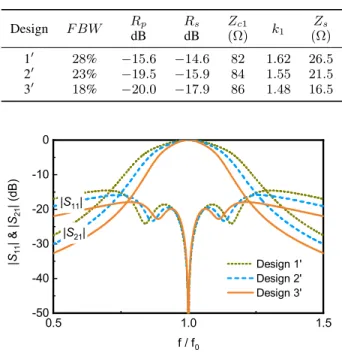
Design F BW Rp dB Rs dB Zc1 (Ω) k1 Zs (Ω) 10 28% −15.6 −14.6 82 1.62 26.5 20 23% −19.5 −15.9 84 1.55 21.5 30 18% −20.0 −17.9 86 1.48 16.5 0.5 1.0 1.5 -50 -40 -30 -20 -10 0 | S 1 1 | & | S 2 1 | ( d B ) f / f 0 Design 1' Design 2' Design 3' |S 21 | |S 11 |
Fig. 10. Improved matching from Fig. 9 by tuning the impedanceZc1.
B. Extension to Higher-Order Quasi-Absorptive BPFs
In conventional reflective-type filters, increasing the filter order is realized by coupling more resonators in the main signal path [35]. Similarly, the proposed quasi-absorptive BPFs architecture can be extended to higher order by increasing
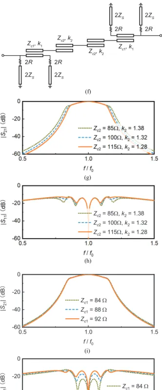
the order of the bandpass section. Fig. 11 (a) and Fig. 11 (f) show examples of a 2-pole and a 3-pole equal-ripple-reflection quasi-absorptive BPFs.Ze2andZo2are the respective coupled
even- and odd-mode impedance of the coupled-line section for higher-order implementation. All the other circuit parameters are the same as Design 2 of Table I, viz., Zc1 = 92 Ω,
Zs= 21.5 Ω,Z0= 50 Ω,R= 50 Ω, andk1= 1.55.
Similar to the 1-pole case, the bandwidth of the higher-order quasi-absorptive filters are primarily determined byZs of the absorptive stubs. The coupled lines in the bandpass section are essentially independent from the quasi-absorptive coupled lines at the input and output of filter. In order words, the bandwidth of the filter is mainly set by the quasi-absorptive coupled lines, while the filter roll-off is mainly set by the bandpass coupled lines. As such, one can simply increase the filter order by cascading more coupled lines sections without affecting the bandwidth of the filter.
Fig. 11 (b)–(c) and Fig. 11 (g)–(h) show the 2-pole and 3-pole filter responses with varied coupled impedanceZc2and
coupling coefficient k2. −13dB equal-ripple reflection level
can be attained for both 2-pole and 3-pole quasi-absorptive BPFs by using the same coupled-line parameters Zc2 and
k2. Similar to the 1-pole quasi-absorptive BPF case, the
in-band reflection can be improved by adjusting Zc1 without
changing the passband FBW, as shown in Fig. 11 (d)–(e) and Fig. 11 (i)–(j).
Frequency responses of the 1-, 2-, and 3-pole quasi-absorptive filters are given in Fig.12 for comparison. The circuit values for 1-pole filter are the same as Design 2 of Table I. The coupled-line parameters for higher-order extensions are identical and set to Zc2 = 100 Ω and
k2 = 1.32. With the same circuit parameters, different-order
quasi-absorptive filters have the same F BW and maintain equal-ripple-reflection responses. However, both the stopband attenuation and passband roll-off are accordingly improved as the order increases. Besides, all-band quasi-reflectionless at both input and output ports can be attained, however, at the cost of deteriorated in-band transmission flatness. The deterioration is due to the fact that the loaded absorption resistors are resonance-dependent and only equivalently opened at the center frequency f0. Future work can be
focused on symmetrical quasi-absorptive BPFs with improved passband transmission flatness by using quasi-absorptive circuits that can be equivalently opened in a wide frequency range.
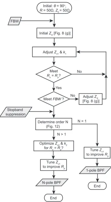
Based on these observations, a step-by-step design guideline can be developed and is illustrated in Fig. 13.
1) The process starts with a set of initial values for θ, R, andZ0. For simplicity, one can set θ= 90◦,Z0= 50 Ω,
andR=Z0= 50 Ω.
2) Because the absorptive sections remain constant in filters with any order, the optimal values of Zs, k1, and Zc1
can be determined using a 1-pole quasi-absorptive BPF with the same bandwidth requirement as the higher-order filter.
a) Based on the bandwidth requirement, an initial value ofZsis determined by parametric analysis of a 1-pole
2R 2R 2Z S 2ZS 2ZS 2R 2ZS 2R Zc 1, k1 Z c1, k1 Zc2, k2 2R 2R 2Z S 2ZS 2ZS 2R 2ZS 2R Z c1, k1 Zc2, k2 Z c2, k2 Z c1, k1 (a) (b) (c) (d) (e) (f) (g) (h) (i) (j)
Fig. 11. 2-pole and 3-pole quasi-absorptive filters. (a) Transmission-line circuit model of the 2-pole quasi-absorptive BPF. (b) Simulated|S21|of the 2-pole
quasi-absorptive BPF for variousZc2andk2. (c) Simulated|S11|of the 2-pole quasi-absorptive BPF for variousZc2andk2. (d) Simulated|S21|of the 2-pole
quasi-absorptive BPF for variousZc1(Zc2= 100 Ωandk2= 1.32). (e) Simulated|S11|of the 2-pole quasi-absorptive BPF for variousZc1(Zc2= 100 Ω
andk2= 1.32). (f) Transmission-line circuit model of the 3-pole quasi-absorptive BPF. (g) Simulated|S21|of the 3-pole quasi-absorptive BPF for various
Zc2 andk2. (h) Simulated|S11|of the 3-pole quasi-absorptive BPF for variousZc2 and k2. (i) Simulated|S21|of the 3-pole quasi-absorptive BPF for
1s t-order 2nd-order 3rd-order
(b)
Fig. 12. Simulated frequency responses of the 1-, 2-, and 3-pole quasi-absorptive filters using the same circuit parameters as in Fig. 11. (a)
|S21|. (b)|S11|.
quasi-absorptive BPF , similar to Fig. 8 (g).
b) Determine Zc1 and k1 to realize an equi-ripple
reflection response in a similar fashion as Fig. 8 (b)–(i). Note that Zc1 needs to be sufficiently large to ensure
that fp2 andfp4 are real valued.
c) Depending on the resulting filter performance from Step b), Zc1, k1, and Zs may need to be slightly adjusted/optimized for an optimal trade-off between bandwidth and reflection level.
3) Once the design of the 1-pole quasi-absorptive BPF is finalized, the required filter order 2N can be determined from Fig. 12 (a) using the 1-pole response as a reference. 4) N coupled lines sections are inserted in the bandpass section to create the N-pole filter. The coupled lines parameters Zc2 and k2 need to be optimized for
equal-ripple reflection. If desired, the passband reflection can be improved by slightly reducingZc1.
C. Comparison With the State-of-the-Art
At the time of writing, only two distributed symmetrical absorptive BPFs have been presented in the literature,
the quasi-absorptive BPFs using complementary
bandstop-bandpass structures in [32] and the fully-absorptive BPF based on the theory of duality in [31]. Representative circuit diagrams of these two circuits are shown in Fig. 14 (a) and Fig. 14 (b). Note that [32] presents a technology-independent coupling matrix formalism to have symmetrical quasi-reflectionless performances. To make a fair comparison, its proof-of-concept microstrip implementation is compared with the proposed distributed quasi-absorptive filters. We also note that in all three filter structures, a bandpass section and a bandstop section can
Initial: θ = 90o, R = 50Ω, Z0 = 50Ω Initial ZS [Fig. 8 (g)] Meet Rs = Rp? Meet FBW ? Stopband suppression Optimize Zc2 & k2 for Rs = Rp? Adjust ZS [Fig. 8 (g)] No Yes No Tune Zc1 to improve Rp Adjust Zc1 & k1 Determine order N (Fig. 12) End FBW N > 1 N-pole BPF 1-pole BPF End N = 1 Tune Zc1 to improve Rp
Fig. 13. Working flow of the design and optimization process.
be clearly identified. Interestingly, without the absorptive sections, the bandpass sections alone exhibit proper reflective filter responses.
Fig. 14 (c) and Fig. 14 (d) compare the transmission and reflection responses of the proposed quasi-absorptive filter [Fig. 6 (a)] and those of [31] and [32]. To make a fair comparison, all three filters are designed for 1-pole response with the same3-dB bandwidth.
The work of [31] is the only one that has fully reflectionless performance at all frequencies. As a result, the simulated|S11|
is 0 and cannot be shown in the dB-scale plot of Fig. 14 (d). The filter also outperforms both this work and the work of [32] in terms of close-in rejection due to the creation of transmission zeros very close to the passband edge. However, the proposed work generally exhibits better rejection than both filters in [31] and [32] at frequencies above approximately
1.3f0.
(a) (b) R R Z r Zr Zr Zr Z r Zr ZC Z C ZB ZB Z A ZA Bandpass section Absorptive section R R Bandpass section Absorptive section Z1 Z1 Z 2 Z2 Z e, Zo Ze, Zo Port 1 Port 2 Port 1 Port 2
Fig. 14. (a) Distributed circuit model of the 1-pole quasi-absorptive BPF in [32]. (b) Distributed absorptive BPF presented in [31]. (c) A comparison of the simulated S21 between the proposed work and those of [32] and [31]. (d) A comparison of the simulatedS11between the proposed work and those of
[32] and [31]. (e)–(g) A comparison of the simulatedS21between the overall absorptive filter and its bandpass section in [31], [32], and this work.
also acknowledged in [30] and [32], is the impractical circuit parameters due to the extremely high transmission-line impedance ratio as well as coupling coefficient of the coupled line sections even for moderate bandwidth. In addition, although a very deep close-in rejection can be created by increasing the order of the absorptive sections, the filter’s far-out-of-band rejection is limited to an equivalent 1-pole response. A higher-order roll-off is yet to be demonstrated. In contrast, the proposed filter structures in this work can realize arbitrarily high orders by cascading more coupled lines in the bandpass sections.
The low reflection and high stopband attenuation for the work of [32] can only hold near the passband. In the lower stopband (centered at dc) and upper stopband (centered at2f0),
the filter degenerates back to a reflective type. In contrast, the design presented in this paper can achieve quasi-absorptive responses across all the frequencies with improved passband selectivity and stopband rejection.
Fig. 14 (e)–(f) show comparative studies of the three filters with and without the absorptive sections. As we demonstrated in Section III-A, the bandwidth of the proposed quasi-absorptive filter structure is much smaller than its bandpass section. We can see that this is true for the work of [32] and to a lesser extent also true for the work of [31].
In both [32] and this work, the much reduced bandwidth means that the filter design must start with a much wider bandpass filter. When realized with coupled lines, this can lead to unwieldy component values. Although the work of [31] exhibits only slightly bandwidth reduction, we should note that it uses two coupled lines sections with signal power coupled from the same side. This configuration is known to result in a very small usable bandwidth, which explains why excessively high coupling coefficient is needed to realize moderate bandwidth in [31].
IV. EXPERIMENTALVALIDATION
To validate the proposed design concepts, a class of quasi-absorptive BPFs with 1-, 2-, and 3-pole responses are designed and implemented on a 0.813-mm-thick Rogers 4003C substrate (relative permittivity of 3.55 and a loss tangent of0.0027). The filters are designed at2.45GHz with a 3-dB fractional bandwidth of22%. Schematic simulations are performed using Keysight Advanced Design System software (ADS) and electromagnetic (EM) simulations are carried out using Ansys High-frequency Structure Simulator (HFSS). Fig. 15 shows the layout, pictures, and the measured frequency responses of the filters.
15.0 1.68 18.4 1.8 0.32 0.32 0.28 19.0 0.3 15.0 1.68 18.4 1.8 0.320.32 0.28 0.55 19.0 0.3 15.0 1.68 18.4 1.8 0.32 0.32 0.28 0.56 19.0 0.3 (a) (f) (k) (b) (g) (m) (c) (h) (n) (d) (i) (o) (e) (j) (p)
Fig. 15. (a) The layout and (b) a picture of the 1-pole quasi-absorptive BPF. (c) Circuit, simulation, and measured|S21|of the 1-pole quasi-absorptive BPF.
(d) Circuit, simulation, and measured|S11|of the 1-pole quasi-absorptive BPF. (e) Measured group delay of the 1-pole quasi-absorptive BPF. (f) The layout
and (g) a picture of the 2-pole quasi-absorptive BPF. (h) Circuit, simulation, and measured|S21|of the 2-pole quasi-absorptive BPF. (i) Circuit, simulation,
and measured|S11|of the 2-pole quasi-absorptive BPF. (j) Measured group delay of the 2-pole quasi-absorptive BPF. (k) The layout and (m) a picture of
the 3-pole quasi-absorptive BPF. (n) Circuit, simulation, and measured|S21|of the 3-pole quasi-absorptive BPF. (o) Circuit, simulation, and measured|S11|
of the 3-pole quasi-absorptive BPF. (p) Measured group delay of the 3-pole quasi-absorptive BPF.
Following the procedures outlined in Fig. 13, the optimized circuit parameters of the 1-pole quasi-absorptive BPF are found to be Zs= 22.5 Ω,Zc1 = 92 Ω,k1= 1.55,R= 50 Ω,
θ = 90◦, and Z0 = 50 Ω for an equi-ripple-reflection
response. Using ADS’s built-in microstrip line primitives, the simulated S11 is better than−17dB up to6.5GHz, covering
both the passband and the stopband. The full-wave simulated
performance is slightly worse in terms of absorption with a worst caseS11 of−14dB. This is primarily because the EM
simulation takes into account the effects of discontinuities in the microstrip structures.
The measured insertion loss [Fig. 15 (c)] is 0.6dB at
2.45GHz, and the measured 3-dB bandwidth is2.2–2.75GHz (F BW = 22.5%). Due to fabrication and component value
tolerances, the measured reflection coefficient [Fig. 15 (d)] is slightly worse than that of the EM simulation. The worst case in-bandS11is−13dB at2.7GHz. The measured group delay
[Fig. 15 (e)] in the passband varies from 3.9ns to 4.3ns, viz., in–band group delay variation smaller than 0.4ns.
The 2-pole filter [Fig. 15 (f)–(g)] is designed by inserting a coupled lines section in the bandpass section. The optimized values for the coupled lines areZc2= 100 Ω andk2 = 1.32.
In the range of 1–6.6GHz, the measured S11 in Fig. 15 (i) is
better than −10.7dB across all frequencies and better than −13.5dB in the passband. The insertion loss at the center frequency is measured to be 0.9dB. The measured 3-dB bandwidth is 2.2–2.78GHz (F BW = 23.6%). The measured group delay [Fig. 15 (j)] within the 3dB passband range is between 4.2ns and 4.9ns, viz., the group delay variation is lower than0.7ns.
The 3-pole filter [Fig. 15 (k)–(m)] is constructed by simply adding another section of coupled lines (Zc2, k2). The
measuredS11 in Fig. 15 (o) is better than−10dB in the range
of 1–6.7GHz. The maximum in-band reflection is measured to be −13.5dB. The measured insertion loss is 1.1dB at
2.45GHz. The measured 3-dB bandwidth is 2.2–2.76GHz (F BW = 22.8%). The measured group delay variation within the 3dB passband range is lower than 0.9ns, i.e., in-band group delay between 4.8ns and5.7ns.
In all three cases, the measured results agree very well with the simulations except at around2f0. In schematic simulations,
full suppression at2f0 can be attained due to the transmission
zeros (fp1 and fp5) from the absorptive coupled lines even
though the bandpass section has spurious transmission at2f0.
In practice, however, parasitics and fabrication tolerances in the practical distributed circuit result in slight deviations of
fp1 and fp5 from 2f0 and a corresponding degradation in
the absorption. Nevertheless, all the simulated and measured results show predicted quasi-absorptive behavior in both passband and stopband, which well validates the proposed absorptive filter design concept. Note that the all-band return loss in the circuit analysis is better than 17dB for the implemented 1-, 2-, and 3-pole filters. In the practical layout implementations, however, it decreases from13dB to10dB as the filter order increases from one to three. Such degradation is due to the increased parasitic effect as the filter order increases and will limit the maximum order of the practical filters.
V. CONCLUSION
In this paper, we have presented a new high-order distributed absorptive bandpass filter design that can achieve two-port quasi-absorptive responses over a wide frequency range. The essential building block of such filters is a coupled lines section loaded with two resonant absorptive stubs. We show that the bandwidth of the proposed absorptive filters are primarily determined by the absorptive coupled lines. As a result, higher-order response can be achieved by simply increasing the order of the bandpass section. A set of quasi-absorptive filters with various orders have been designed and measured to validate the proposed absorptive filter design methodology.
ACKNOWLEDGEMENT
The authors would like to thank Prof. A. A. Melc´on, Department of Information and Communication Technologies, Technical University of Cartagena, Murcia, Spain, for his helpful discussions.
REFERENCES
[1] Mini-Circuits Inc., “Reflectionless filters improve linearity and dynamic range,” Microwave Journal, 2015. [Online]. Available: http://www.microwavejournal.com/articles/ 24825-reflectionless-filters-improve-linearity-and-dynamic-range [2] H. Uchida, K. Yamanaka, K. Yamauchi, A. Inoue, and Y. Hirano, “A
reflection-absorptive harmonic-rejection filter for RF power amplifiers,” inThe 40th European Microwave Conference, Sep. 2010, pp. 763–766. [3] M. A. Morgan, “Think outside the band: Design and miniaturization of absorptive filters,”IEEE Microw. Mag., vol. 19, no. 7, pp. 54–62, Nov. 2018.
[4] W. D. Lewis and L. C. Tillotson, “A non-reflecting branching filter for microwaves,”Bell Sys. Tech. J., vol. 27, no. 1, pp. 83–95, Jan. 1948. [5] S. B. Cohn and F. S. Coale, “Directional channel-separation filters,”
Proc. IRE, vol. 44, no. 8, pp. 1018–1024, Aug. 1956.
[6] F. S. Coale, “A traveling-wave directional filter,”IRE Trans. Microw. Theory Techn., vol. 4, no. 4, pp. 256–260, Oct. 1956.
[7] J. P. Kim, “Improved design of single-section and cascaded planar directional filters,”IEEE Trans. Microw. Theory Techn., vol. 59, no. 9, pp. 2206–2213, Sep. 2011.
[8] Y. Cheng, W. Hong, and K. Wu, “Half mode substrate integrated waveguide (HMSIW) directional filter,” IEEE Microw. Compon. Lett., vol. 17, no. 7, pp. 504–506, Jul. 2007.
[9] D. Psychogiou and R. G´omez-Garc´ıa, “Reflectionless adaptive rf filters: Bandpass, bandstop, and cascade designs,”IEEE Trans. Microw. Theory Techn., vol. 65, no. 11, pp. 4593–4605, Nov. 2017.
[10] D. J. Simpson, R. G´omez-Garc´ıa, and D. Psychogiou, “Mixed-technology quasi-reflectionless planar bandpass filters,” in
Proc. 48th Eur. Microw. Conf. (EuMC), Sep. 2018, pp. 551–554. [11] M. Khalaj-Amirhosseini and M. Taskhiri, “Twofold reflectionless filters
of inverse-chebyshev response with arbitrary attenuation,”IEEE Trans. Microw. Theory Techn., vol. 65, no. 11, pp. 4616–4620, Nov. 2017. [12] R. G´omez-Garc´ıa, J. Mu˜no-erreras, and D. Psychogiou, “Split-type
input-reflectionless multiband filters,” IEEE Microw. Compon. Lett., vol. 28, no. 11, pp. 981–983, Nov. 2018.
[13] R. G´omez-Garc´ıa, J. Mu˜noz-Ferreras, and D. Psychogiou, “Rf reflectionless filtering power dividers,” IEEE Trans. Circuits Syst. II, Express Briefs, pp. 1–1, 2018.
[14] ——, “Dual-behavior resonator-based fully reconfigurable input reflectionless bandpass filters,” IEEE Microw. Compon. Lett., vol. 29, no. 1, pp. 35–37, Jan. 2019.
[15] ——, “Tunable input-quasi-reflectionless multiplexers,” inIEEE MTT-S Int. Microw. Workshop Ser. 5G Hardw. Syst. Technol. (IMWS-5G), Aug. 2018, pp. 1–3.
[16] ——, “Symmetrical quasi-reflectionless BSFs,”IEEE Microw. Compon. Lett., vol. 28, no. 4, pp. 302–304, Apr. 2018.
[17] R. G´omez-Garc´ıa, J. Mu˜noz-Ferreras, W. Feng, and D. Psychogiou, “Balanced symmetrical quasi-reflectionless single-and dual-band bandpass planar filters,”IEEE Microw. Compon. Lett., vol. 28, no. 9, pp. 798–800, Sep. 2018.
[18] J. Lee, T. C. Lee, and W. J. Chappell, “Lumped-element realization of absorptive bandstop filter with anomalously high spectral isolation,”
IEEE Trans. Microw. Theory Techn., vol. 60, no. 8, pp. 2424–2430, Aug. 2012.
[19] J. Shao and Y. Lin, “Narrowband coupled-line bandstop filter with absorptive stopband,” IEEE Trans. Microw. Theory Techn., vol. 63, no. 10, pp. 3469–3478, Oct. 2015.
[20] M. Kong, Y. Wu, Z. Zhuang, Y. Liu, and A. A. Kishk, “Compact wideband reflective/absorptive bandstop filter with multitransmission zeros,”IEEE Trans. Microw. Theory Techn., vol. 67, no. 2, pp. 482–493, Feb. 2019.
[21] A. C. Guyette, I. C. Hunter, R. D. Pollard, and D. R. Jachowski, “Perfectly-matched bandstop filters using lossy resonators,” in IEEE MTT-S Int. Microw. Symp. Dig., Jun. 2005, pp. 4 pp.–520.
[22] T. Lee, B. Kim, K. Lee, W. J. Chappell, and J. Lee, “Frequency-tunable low-qlumped-element resonator bandstop filter with high attenuation,”
IEEE Trans. Microw. Theory Techn., vol. 64, no. 11, pp. 3549–3556, Nov. 2016.
[23] A. C. Guyette, E. J. Naglich, and S. Shin, “Switched allpass-to-bandstop absorptive filters with constant group delay,” IEEE Trans. Microw. Theory Techn., vol. 64, no. 8, pp. 2590–2595, Aug. 2016.
[24] M. D. Hickle and D. Peroulis, “Theory and design of frequency-tunable absorptive bandstop filters,”IEEE Trans. Circuits Syst. I, Reg. Papers, vol. 65, no. 6, pp. 1862–1874, Jun. 2018.
[25] P. Adhikari, W. Yang, Y. Wu, and D. Peroulis, “A pcb technology-based 2242-ghz quasi-absorptive bandstop filter,”IEEE Microw. Compon. Lett., vol. 28, no. 11, pp. 975–977, Nov. 2018.
[26] A. R. Djordjevic, A. G. Zajic, A. S. Stekovic, M. M. Nikolic, Z. A. Maricevic, and M. F. C. Schemmann, “On a class of low-reflection transmission-line quasi-Gaussian low-pass filters and their lumped-element approximations,”IEEE Trans. Microw. Theory Techn., vol. 51, no. 7, pp. 1871–1877, Jul. 2003.
[27] J. Breitbarth and D. Schmelzer, “Absorptive near-gaussian low pass filter design with applications in the time and frequency domain,” inIEEE MTT-S Int. Microw. Symp. Dig., vol. 3, Jun. 2004, pp. 1303–1306. [28] S. Jeong, T. Lee, and J. Lee, “Absorptive filter prototype and
distributed-element absorptive bandpass filter,” inProc. IEEE MTTS Int. Conf. Numer. Electromagn. Multiphys. Model. Optim. (NEMO), Aug. 2018, pp. 1–4.
[29] M. A. Morgan and T. A. Boyd, “Theoretical and experimental study of a new class of reflectionless filter,”IEEE Trans. Microw. Theory Techn., vol. 59, no. 5, pp. 1214–1221, May 2011.
[30] M. A. Morgan, W. M. Groves, and T. A. Boyd, “Reflectionless filter topologies supporting arbitrary low-pass ladder prototypes,”IEEE Trans. Circuits Syst. I, Reg. Papers, vol. 66, no. 2, pp. 594–604, Feb. 2019. [31] M. A. Morgan and T. A. Boyd, “Reflectionless filter structures,”IEEE
Trans. Microw. Theory Techn., vol. 63, no. 4, pp. 1263–1271, Apr. 2015. [32] R. G´omez-Garc´ıa, J. Mu˜noz-Ferreras, and D. Psychogiou, “Symmetrical quasi-absorptive RF bandpass filters,” IEEE Trans. Microw. Theory Techn., vol. 67, no. 4, pp. 1472–1482, Apr. 2019.
[33] D. M. Pozar,Microwave Engineering. Wiley, 2012.
[34] E. M. T. Jones, “Coupled-strip-transmission-line filters and directional couplers,”IRE Trans. Microw. Theory Techn., vol. 4, no. 2, pp. 75–81, Apr. 1956.
[35] J.-S. Hong and M. J. Lancaster,Microstrip Filters for RF / Microwave Applications. Wiley, 2001.
Xiaohu Wu (M’15–SM’19) was born in Hubei, China, in 1987. He received the B.Eng. degree in information engineering and Ph.D. degree in electromagnetic fields and microwave technology from South China University of Technology, Guangzhou, China, in 2008 and 2013, respectively. His Ph.D. dissertation concerned the exploration of multimode resonators and their applications to filter designs.
From June 2013 to July 2014, he worked as an engineer on scalable active array in the East China Research Institute of Electronic Engineering (ECRIEE), Hefei, China. In 2015, he joined the School of Electronic and Information Engineering, Nanjing University of Information Science and Technology, Nanjing, China, as an assistant professor. Sine October 2017, he has been a post-doctoral researcher with the Department of Electrical and Computer Engineering, University of California, Davis, CA, USA. His current research interests include time-varying non-reciprocal devices and absorptive circuit designs.
Yingsong Li(S’09–M’14–SM’19) received his B.S. degree in electrical and information engineering in 2006, and M.S. degree in Electromagnetic Field and Microwave Technology from Harbin Engineering University, 2006 and 2011, respectively. He received his Ph.D degree from both Kochi University of Technology (KUT), Japan and Harbin Engineering University, China in 2014. He is a visiting scholar of University of California, Davis from March 2016 to March 2017. Now, he is a full professor of Harbin Engineering University from July 2014. He is also a visiting professor of Far Eastern Federal University (FEFU) and KUT. He is a senior of Chinese Institute of Electronics (CIE), member of IEEE. He is an Associate Editor of IEEE Access, Applied Computational Electromagnetics Society Journal, and AE ¨U-International Journal of Electronics and Communications.
Dr. Li also serves as a reviewer for more than 20 journals. Recently, his recent research interests are mainly in remote sensing, underwater communications, signal processing, radar, SAR imaging, compressed sensing and antennas.
Xiaoguang “Leo” Liu(M’10–SM’16) received his Bachelors degree from Zhejiang University in 2004 and PhD degree from Purdue University, USA in 2010. He joined the Department of Electrical and Computer Engineering, University of California, Davis in Nov. 2011 as an assistant professor and was promoted to an associate professor in Jul. 2017. At UC Davis, his research group is investigating various aspects of cutting-edge high-frequency and high-speed circuit and system designs. Examples include novel designs and implementation techniques in microelectronic and photonic devices such as micro-electromechanical (MEMS) devices, high-frequency (RF to THz) circuit designs, high-speed wireline and optical communications, high-precision sensing using radar and laser time-of-flight (ToF) principles, antennas and passive components. His research group’s website is https://dart.ece.ucdavis. edu/.


![Fig. 5. Comparisons of the singly-loaded [Fig. 2 (b)] and the doubly-loaded [Fig. 2 (c)] quasi-absorptive coupled lines in terms of calculated S-parameters (Z c1 = 98 Ω, Z s = 21.5 Ω, k 1 = 1.63, R = 50 Ω, Z 0 = 50 Ω): (a) |S 11 |, (b) |S 22 |, and (c) |S](https://thumb-us.123doks.com/thumbv2/123dok_us/1870965.2773063/6.918.95.424.95.737/comparisons-singly-loaded-doubly-absorptive-coupled-calculated-parameters.webp)
![Fig. 14. (a) Distributed circuit model of the 1-pole quasi-absorptive BPF in [32]. (b) Distributed absorptive BPF presented in [31]](https://thumb-us.123doks.com/thumbv2/123dok_us/1870965.2773063/12.918.105.811.84.595/distributed-circuit-model-quasi-absorptive-distributed-absorptive-presented.webp)
