...
DZV11 asynchronous
multiplexer
user's guide
DZV11 asynchronous
multiplexer
user's guide
Copyright © 1978 by Digital Equipment Corporation
The material in this manual is for informational purposes and is subject to change without notice.
Digital Equipment Corporation assumes no respon-sibility for any errors which may appear in this manual.
Printed in U.S.A.
This document was set on DIGITAL's DECset-8000 computerized typesetting system.
The following are trademarks of Digital Equipment Corporation, Max-nard, Massachusetts:
DEC DECCOMM DECsystem·lO DECSYSTEM·20
DECtape
D~CUS
DIGITAL MASSBUS
PDP RSTS TYPESET·8 TYPESET·ll UNIBUS
CHAPTER 1 1.1 1.2 1.2.1 1.2.2 1.2.3 1.3 1.3.1 1.3.2 1.3.3 1.3.3.1 1.3.3.2 1.3.3.3 1.3.3.4 1.3.3.5 1.3.3.6 1.3.4
CHAPTER 2
2.1 2.2 2.3 2.3.1 2.3.1.1 2.3.1.2 2.3.2
CHAPTER 3
3.1 3.2 3.2.1 3.2.2 3.2.3 3.2.4
CONTENTS
PageGENERAL DESCRIPTION
INTRODUCTION ... 1-1
PHYSICAL DESCRIPTION ... 1-1
DZVll Configurations ... 1-1
BC 11 U Interface Cable ... 1-4
Test Connectors ... 1-5
SPECIFICATIONS ... 1-5
Environmental ... 1-5
Electrical ... 1-5
Performance-...
f-5
Maximum Configurations ... 1-5
Throughput. ... 1-7
Receivers ... 1-7
Transmitters ... 1-7 Baud Rate Generator ... 1-7
Performance Summary ... 1-7
Interrupts ... 1-7
INSTALLATION
SCOPE ... 2-1
UNPACKING AND INSPECTION ... 2-1
INSTALLATION PROCEDURE ... 2-1
Jumper Configuration ... 2-1
Device Operation ... 2-1
Modem Control Jumpers ... 2-3
Module Installation ... 2-3
DEVICE REGISTERS
SCOPE ... 3-1
DEVICE REGISTERS ... 3-1
Control and Status Register ... 3-1
Receiver Buffer ... 3-1
Line Parameters Register ... 3-5
CHAPTER 4 4.1 4.2 4.3 4.4 4.4.1 4.4.2 4.4.3 4.4.4 4.4.5 4.4.6 4.4.7 4.4.8 APPENDIX A Figure No. 1-1 1-2 1-3 1-4 1-5 2-1 2-2 2-3 3-1 Table No. 2-1 2-2 2-3 2-4 3-1 3-2 3-3 3-4 4-1
CONTENTS (Cont)
Page PROGRAMMINGSCOPE ... 4-1 DEVICE ADDRESS ASSIGNMENTS ... .4-1 INTERRUPT VECTOR ADDRESS ASSIGNMENTS ... .4-1 PROGRAMMING FEATURES ... 4-2 Baud Rate ... 4-2 Character Length ... 4-2 Stop Bits. '" ... 4-3 Parity ... 4-3 Interrupts ... 4-3 Emptying the Silo ... 4-4 Transmitting a Character ... 4-4 Data Set Control ... 4-5
GLOSSARY A-I
FIGURES
Title Page
DZVI1-A (M7957 Module) ... 1-2 DZV II System Applications ... 1-3 DZVII-B (M7957 Module, H325 and H329 Connectors and
Cable Assembly BCll U-25) ... 1-4 Test Connectors H325 and H329 ... 1-5 Loopback Connections ... 1-6 M7957 Jumper Locations ... 2-2 M7957 Address Selection ... 2-4 M7957 Vector Selection ... 2-4 Register Bit Assignments ... 3-2
TABLES
Title Page
Items Supplied per Configuration ... 2-1 Jumper Configuration ... 2-3 M7957 Vector Address Switch Selection ... 2-4 Vector Switch Selection ... 2-5 DZVII Register Address Assignments ... 3-1 CSR Bit Assignments ... 3-3 RBUF Bit Assignments ... 3-5 LPR Bit Assignments ... 3~6
Baud Rate Selection Chart ... 4-2
1.1 INTRODUCTION
CHAPTER 1
GENERAL DESCRIPTION
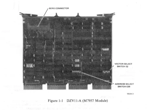
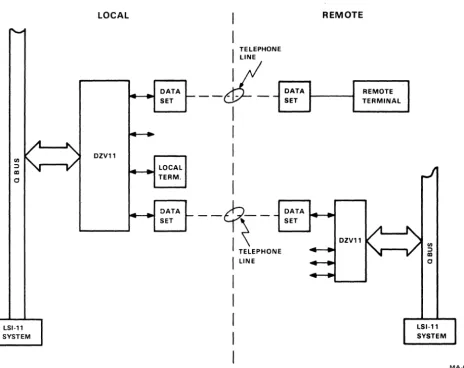
The DZVII, shown in Figure I-I, is an asynchronous multiplexer that provides an interface between an LSI-II processor and four asynchronous serial data communication channels. It can be used with the LSI-II processor in a variety of applications that include data concentration, real time processing and cluster controlling. The DZVII provides an EIA RS232C interface and enough data set control to permit dial-up (auto answer) operation with modems capable of full-duplex operation*, such as the Bell models 103, 113, 212, or equivalent. Remote operation over private lines for full-duplex point to point or full-duplex multipoint as a control (master) station is also possible. Figure 1-2 depicts several of the possible applications for the DZVII in an LSI-II system.
Figure I-I DZVII-A (M7957 Module)
VECTOR SELECT SWITCH E2
ADDRESS SELECT SWITCH E30
[image:6.611.55.547.311.667.2]CI.I
~
CD
d
LOCAL
DZV11
DATA SET
LOCAL TERM.
DATA SET
I
TELEPHONELINE
--It-
-I
I
I
I
I
DATA SET
__
~
__
~:;A
I
TELEPHONEI
LINEREMOTE
REMOTE TERMINAL
DZV11
Figure 1-2 DZVl1 System Applications
MA·0553
The DZVll has several features that provide flexible control of parameters such as baud rate, charac-ter length, number of stop bits for each line, odd or even parity for each line, and transmitcharac-ter-receiver interrupts. Additional features include limited data set control, zero receiver baud rate, break gener-ation and detection, silo buffering of received data, and line turnaround.
Program compatibility is maintained with the Unibus option DZII-A. The only compatibility excep-tion is the number of serial channels supported. The DZVll does not support 20 rnA operaexcep-tion.
1.2 PHYSICAL DESCRIPTION
The DZVll comprises a single quad size module, 21.6 cm X 26.5 cm (8.51 inches X 10.44 inches), and is designated as the M7957 module. All input and output leads are available on a Berg header. The DZVll connects to the LSI-II QBUS by the H9270 mounting panel or equivalent. All QBUS in-put/ output signals enter and leave the module via the mounting panel pins.
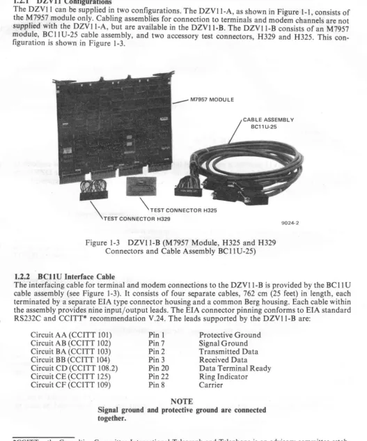
[image:7.620.78.542.49.417.2]1.2.1 DZVll Configurations
The DZVll can be supplied in two configurations. The DZVII-A, as shown in Figure 1-1, consists of the M7957 module only. Cabling assemblies for connection to terminals and modem channels are not supplied with the DZVII-A, but are available in the DZVI1-B. The DZVII-B consists of an M7957
modul~, B~ II U-25 .cable assembly, and two accessory test connectors, H329 and H325. This con-figuratIOn IS shown III Figure 1-3.
M7957 MODU LE
\ TEST CONNECTOR H325
TEST CONNECTOR H329
Figure 1-3 DZVl1-B (M7957 Module, H325 and H329
Connectors and Cable Assembly BC 11 U -25)
1.2.2 BCII U Interface Cable
9024-2
The interfacing cable for terminal and modem connections to the DZVl1-B is provided by the BCll U cable assembly (see Figure 1-3). It consists of four s~parate cables, 762 cm (25 feet) in length, each terminated by a separate EIA type connector housing and a common Berg housing. Each cable within the assembly provides nine input/output leads. The EIA connector pinning conforms to EIA standard RS232C and CCITT* recommendation V.24. The leads supported by the DZVII-B are:
Circuit AA (CCITT 101) Circuit AB (CCITT 102) Circuit BA (CCITT 103) Circuit BB (CCITT 104) Circuit CD (CCITT 108.2) Circuit CE (CCITT 125) Circuit CF (CCITT 109)
Pin 1 Pin 7 Pin 2 Pin 3 Pin 20 Pin 22 Pin 8
NOTE
Protective Ground Signal Ground Transmitted Data Received Data
Data Terminal Ready Ring Indicator
Carrier
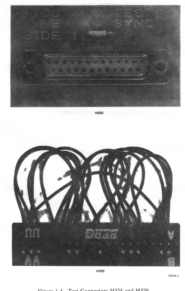
[image:8.614.43.570.48.681.2]1-.2.3 Test Connectors
Figure 1-4 shows the two accessory test connectors, H329 and H325, that are provided with each DZVII-B. The H325 plugs into an EIA connector on the BC11 U to loopback data and modem signals onto a single line. The H329 plugs into the M7957 module socket housing and provides staggered loop back of the data and modem lines. The loopback connections are shown in Figure 1-5.
1.3 SPECIFICA TIONS
Environmental, electrical, and performance specifications for the DZVll are discussed in the follow-ing paragraphs.
1.3.1 Environmental
The DZV11 operates in an environment from 50 to 500 C (41 0 to 1220 F) and in a relative humidity of 10% to 95%.
1.3.2 Electrical
Power Consumption 1.15 A@ +5 Vdc
0.39 A@ +12 Vdc
For each line the DZV11 provides a voltage level interface whose levels and connections conform to EIA standard RS232C and CCITT recommendation V.24. The leads supported by the DZVl1 are listed in topic 1.2.2. Each DZVll meets the LSI-ll QBUS Interface specification and represents one unit load as an interface.
1.3.3 Performance
The following paragraphs describe the DZV11 performance capabilities and restrictions.
1.3.3.1 Maximum Configurations - The DZV11 multiplexer is assigned a device address in the float-ing address space. The floatfloat-ing address space starts at 760010 and extends to 764000. A maximum configuration of DZV11s would not be limited by floating address space, but would be limited by the rules governing an intermediate size system configuration. Therefore, a maximum of seven DZV11 multiplexers may reside in a nine by four backplane.
1.3.3.2 Throughput - Each DZVll is capable of a throughput rate of 10,970 characters per second. This rate is calculated as follows:
(Bits/Second X No. Lines X Direction) divided by Bits/Character. (9600 X 4 X 2) 1/7 equals 10,970 Characters/Second.
For a character service routine of 100 J.LS or less, the device throughput rate can be sustained.
1.3.3.3 Receivers - The receivers provide serial to parallel conversion of 5,6, 7, 8 level code with one start space and at least one stop mark. The character length, number of stop bits, parity generation and operating speed are programmable parameters for each line. A receiver and transmitter of a corre-sponding line share the same operating speed with provisions for enabling/disabling of that receive line.
Each receiver is double-buffered and has an allowable input distortion of 43.75% on any bit. Also, the
ac~umulated character distortion must not exceed 43.75%. Break d~tection is provided on each re-ceIver.
H325
H329
9024-1
[image:10.611.123.489.49.624.2]NOTE:
H329 STAGGERED TURNAROUND
TRANSMIT 0 - - - -... RECEIVE 1
DTR 0
---or--....
:
RING 1... --4.
CARRIER 1RING 0 :
CARRIER 0 ... t--~--- DTR 1
RECEIVE O ....
t---
TRANSMIT 1LINES 2&3 ARE STAGGERED IN THE SAME WAY.
. . . . .
-H325 LOOPBACK CONNECTIONS
S C E 3 2 4
15
SCT
SCR 17
11
SECXMIT~
12
SEC RCV
XMITDATA~
RCVDATA~
4
R E Q T O S E N D 3
ClR TO SEND
8
CARRIER
NEW SYNC 14
:I
6 DATA SET RDY
20
DTR
J
22
RING
0
JUMPER REMOVED
0
Figure 1-5 Loopback Connections
1-6
[image:11.626.182.367.287.610.2]1.3.3.4 Transmitters - The transmitters provide parallel to serial conversion of 5, 6, 7, 8 level code with or without parity. The parity sense when selected can be either odd or even. The stop code can be either 1 or 2 units except when 5 level code is selected. When 5 level code is selected, the stop code can be set to 1 or 1.5 units. The character length, number of stop units, parity generation and sense, and operating speed are programmable parameters for each line. The operating speed for the transmitter is common with the receiver. Breaks are capable of being transmitted on any line. The gross start-stop distortion for a transmitter's TTL output will be less than 2.5% for an 8-bit character.
1.3.3.5 Baud Rate Generator - The baud rate generator is a MOS/LSI device which provides the DZV11 multiplexer with full programmable capability for operating speed selection. Each line has an independent generator capable of producing 1 of 15 selectable baud rates. Speed tolerance for all rates is less than 0.3% with a clock duty of 50%
±
5%. (See below for rates.)1.3.3.6 Performance Summary - The following summarizes the programmable features offered for each line:
Character length
Number of stop bits
Parity
Baud rates
Breaks
1.3.4 Interrupts
5, 6, 7, or 8 level code
1 or 2 for 6, 7, 8 level code 1 or 1.5 for 5 level code
odd, even or none
50, 75, 110, 134.5, 150, 300, 600, 1200, 1800, 2000, 2400, 3600, 4800, 7200, and 9600
Can be generated and detected on each line.
The following interrupts are available on DZV11.
Receiver Done Interrupt
Occurs every time a character appears at the output of the receiver buffer register and the Silo Alarm is disabled. Can be enabled or disabled from the bus.
Silo Alarm Interrupt
Occurs after 16 entries have been made into the receive buffer register by the scanner. This interrupt disables Receiver Done Interrupt and is rearmed when the receive buffer register has been read.
Transmit Interrupt
2.1 SCOPE
CHAPTER 2
INSTALLATION
This chapter contains the procedures for the unpacking, installation, and initial checkout of the DZV11 Asynchronous Multiplexer:
2.2 UNPACKING AND INSPECTION
The DZV 11 is packaged in accordance with commercial packaging practices. First, remove all packing material and check the equipment against the shipping list. (Table 2-1 contains a list of supplied items per configuration.) Report damage or shortages to the shipper immediately and notify the DIGITAL representative. Inspect all parts and carefully inspect the module for cracks, loose components, and separations in the etched paths.
Table 2-1 Items Supplied per Configuration
Quantity Description A B
1 M7957 module X X
1 BC11 U-25 cable assembly X
1 H329 test connector X
1 H325 test connector X
1 Print set (B-TC-DZV11-0-1) X X
DZV11-A and-B Order number MPOO462
1 Software kit ZJ251-RB X X
1 DZVll User's Guide X X
(EK-DZV11-UG)
2.3 INSTALLATION PROCEDURE
The following paragraphs describe the installation of the DZV11 option in an LSI-II system.
2.3.1 Jumper Configuration
There are 16 machine-insertable jumpers on the M7957 module (Figure 2-1).
[image:14.617.116.467.356.527.2]W2 W1
~~
F=l::::::
W4 8~W3
W9*
W12*
l
c:::=J'--~
_---'I
'--~
_---'
',--~
_---'I
'--~
_----'
/c:::=J
r
1 \
W13* W14* W15* W16*
A12 A3 VB V3
woooo~oo~ol
w~m~oom
W10* W11" ADDRESS SWITCHES VECTOR SWITCHES
~cL
*NOTES:
JUMPERS W9, W12, W13, W14, W15, AND W16 ARE REMOVED ONLY FOR MANUFAC-TURING TESTS. THEY SHOULD NOT BE RE~/OVED IN THE FIELD.
JUMPERS W10 AND W11 MUST REMAIN INSTALLED WHEN THE MODULE IS USED IN A BACKPLANE THAT SUPPLIES LSI-11 BUS SIGNALS TO THE C AND D CONNECTORS OF THE DZV11 (SUCH AS THE H9270). WHEN THE MODULE IS USED IN A BACK-PLANE THAT INTERCONNECTS THE C AND D SECTIONS TO AN ADJACENT MODULE, JUMPERS W10 AND W11 MUST BE REMOVED.
[image:15.618.59.540.85.479.2]MK-0064
Figure 2-1 M7957 Jumper Locations
2.3.1.2 Modem Control Jumpers - There are eight jumpers used for modem control. The jumpers labeled WI through W4 connect Data Terminal Ready (DTR) to Request To Send (RTS). This allows the DZVll to assert both DTR and RTS if using a modem that requires control of RTS. These jumpers must be installed to run the cable and external test diagnostic programs. The remaining four jumpers, W5 through W8, connect the Forced Busy (FB) leads to the RTS leads. With these jumpers installed, the assertion of an RTS lead places an ON or BUSY signal on the corresponding Forced Busy lead. The Forced Busy jumpers (W5 through W8) are normally cut out unless the modem re-quires them (Table 2-2).
Table 2-2 Jumper Configuration
Jumper Connection Line
WI DTR to RTS 03
W2 DTR to RTS 02
W3 DTR to RTS 01
W4 DTR to RTS 00
W5 RTS to FB 03
W6 RTS to FB 02
W7 RTSto FB 01
W8 RTSto FB 00
2.3.2 Module Installation
To install the M7957 module, perform the following.
1. Refer to Paragraph 4.2 for descriptions of the address assignments. Set the switches at E30 so that the module responds to its assigned address. When a switch is closed (ON), a binary 1 is decoded. When a switch is open (OFF), a binary 0 is decoded. Note that the switch labeled 1 corresponds to address bit 12,2 corresponds to address bit 11, etc. ( Figure 2-2 and Table 2-3).
2. Vector selection is accomplished by the 8-position switch at E2. Switch positions 7 and 8 are not used. Switch position 6 corresponds to vector bit 3, 5 corresponds to vector bit 4, etc. When a switch is closed (ON), a binary 1 is decoded. When a switch is open (OFF), a binary
o
is decoded (Figure 2-3 and Table 2-4).3. If the module is part of the DZVII-A option, perform step 3. If it is a part of the DZVII-B option, proceed to step 4 for testing.
a. Insert the module in a quad QBus slot of the backplane.
CAUTION
Insert and remove modules slowly and carefully to avoid snagging module components on the card guides and changing switch settings inadvertently.
[image:16.621.182.410.179.332.2]E30 Switch Address 160000 160010 160020 160030 160040 160050 160060 160070 160100 163760 163770 X NOTE:
ADDRESS SELECTOR
A12 A11 A10 A09 AOa A07 A06 A05 A04 A03 ON 1 2 3 4 5 6 7 a 9
[image:17.620.146.479.75.146.2]OFF
I I
I
I
I
I
I
I
I
Figure 2-2 M7957 Address Selection
I 2
AI2 All
-
--
--
--
--
--
--
-~--
--
--
-X =ON
- =
OFFI
~:F
Table 2-3 Address Switch Selection
3 4 5 6 7
AIO A9 A8 A7 A6
-
-
-
-
--
-
-
-
--
-
-
-
--
-
-
-
--
-
-
-
--
-
-
-
--
-
-
-
--
-
-
-
--
-
-
-
XX X X X X
-
X X X XVECTOR SELECTOR
NOT voa V07 V06 V05 V04 V03 USED
2 3 4 5 6 7 a
I
I
I I I I
I
Figure 2-3 M7957 Vector Selection
2-4
10 SWITCH
I
E30'IIA-0915
8 9
A5 A4
-
--
--
X-
XX
-X
-X X
X X
-
-X X
X X
I
S~~TCH
[image:17.620.89.524.227.554.2]E2 Switch Vector 300 310 320 330 340 350 360 370 400 760 770 NOTE:
Table 2-4 Vector Switch Selection
1 V08
-X X XX
=
ON- =
OFF 2 V07 X X X X X X X X -X X3 4
V06 V05
X
-X
-X
-X
-X X
X X
X X
X X
-
-X X
X X
5 6
V04 V03
-
-- X
X
-X X
-
-- X
X
-X X
-
-X
-X X
4. Insert the H329 test connector in J 1 with the letter side facing up. J I is the cable connector at the top of the M7957 module.
5. Insert the module in a quad QBus slot of the backplane.
CAUTION
Insert and remove modules slowly and carefully to avoid snagging module components on the card guides and changing switch settings inadvertently.
Run the DZVII diagnostics, MAINDECs DVDZA and DVDZB, in the staggered mode to verify module operation. Refer to the diagnostic listing for the correct procedure. Run at least three passes without error.
6. Replace the H329 test connector with the Berg end of the BCII U cable assembly. Observe the "This Side Up" wording on the assembly. Refer to D-UA-DZVII-O-O for installation help.
7. Connect the H325 test connector on the first line and run MAINDEC DVDZC. Select the cable test portion of the diagnostic. Three passes are required without error. Repeat this step for each line.
[image:18.618.132.510.62.339.2]sys-9. The DZV 11 is now ready for connection to external equipment. If the connection is to a local terminal through the DZVII-B option, a null modem cable assembly must be used. Use the BC03M or BC03P null modem cables for connection between the BCII U and the terminal. The H312-A null modem unit may also be used in place of the null modem cables.
If connection is to a Bell 103 or equivalent modem, install the appropriate line of the BCll U connector into the connector on the modem. A BC05D cable may be required between the BC II U and the modem. Refer to Paragraph 2.3.1.2, Modem Control Jumpers, for selection of jumpers for modem options such as RTS and forced busy. All of the cables mentioned, excluding the BCll U, must be ordered separately as they are not components of a standqrd DZV II shipment. When possible, run the diagnostic DVDZC in echo test mode to verify the cable connections and the terminal equipment.
,
3.1 SCOPE
CHAPTER 3
DEVICE REGISTERS
This chapter provides a description of each DZVll register, its format, and bit functions.
3.2 DEVICE REGISTERS
The DZV11 contains six addressable registers. A comprehensive pictorial of these registers' bit assign-ments is shown in Figure 3-1. Table 3-1 lists the registers and associated DZVll addresses.
Table 3-1 DZVll Register Address Assignments
Program
Register Mnemonic Address Capability
Contiol and Status Register CSR 76XXXO Read/Write
Receiver Buffer RBUF 76XXX2 Read Only
Line Parameter Register LPR 76XXX2 Write Only
Transmitter Control Register TCR 76XXX4 Read/Write
Modem Status Register MSR 76XXX6 Read Only
Transmit Data Register TDR 76XXX6 Write Only
xxx
=
Selected in accordance with floating device address scheme.3.2.1 Control and Status Register
The control and status register (CSR) is a byte and word addressable register. All bits in the CSR are cleared by an occurrence of BINIT or by setting device Master Clear (CSR 04). The format is shown in Figure 3-1 and the bit assignments are listed in Table 3-2.
3.2.2 Receiver Buffer
[image:20.618.64.545.322.457.2]MSB
15 14 13 12 11 10 09
DR2
{
i - - -RO RW RO RWr'!fl-1 - - -t - - - - :
-bf
trJ
CONTROL O~
TLiNE
& STATUS TRDY TIE SA SAE ~ ~"
.:> ~ B (CSR)
RO RO RO RO RO
1----r--- 1 " - - -
---fi
,
RECEIVER DATA OVRN FRAM PAR RX
BUFFER VALID ERR ERR ERR
~ ~ LINE
(RBUF) B
-<
WO WO WO WO
fi
~
ltt
- - - ----LINE RX SPEED SPEED SPEED
PARAMETER ~ () ENAB CODE CODE CODE
~ ~
(LPR) ~ .;;;,'? D C B
>
I
RW RW RWJi
~
I
---
--TRANSMIT
S'~
1
CONTROL ~O Q~"
~" ~ DTR DTR DTR~"
(TCR) .::> ~ ~ 3 2 1
RO RO RO
tff
,
li li
---
r- -.MODEM ~~ ~~ ~O~ ~O~
STATUS ;;;," ~ .;;;," ~" CO CO CO
(MSR) 3 2 1
..
WO WO WO
,
~
~
tI
i - - - t - - - i-TRANSMIT ~O ~ ~~ ~O~
DATA ~"
~"
;;;," ;;;," BRK BRK BRK(TOR) 3 2 1
'-DRO
DR4
[image:21.1232.59.703.122.515.2]DR6
Figure 3-1 Register Bit Assignments
3-2
BYTES HIGH LOW 08 07
RO
--
RO TLiNEiRDONE A
RO RO
---RX
LINE RBUF
A D7
WO WO
---SPEED ODD CODE PAR
A
RW
~
DTR
~"
~
0
RO
,
--
~~CO ~
0
WO WO
i- - - -
--BRK TBUF
0 7
06 05 04
RW
B.VL_
RW---RIE MSE CLR
RO RO RO
--- ---
----RBUF RBUF RBUF
D6 D5 D4
WO WO WO
---
-PAR STOP CHAR ENAB CODE LGTH B
~
~" ~,
~"
~JI
;;;,",
~
,
~~ ~ ~~ ~ ~"
WO WO WO
---TBUF TBUF TBUF
6 5 4
LSB
03 02 01 00
i-!!..W _ _
trJ
~ Qt%
~()~
MAINT .:> ~ ~ ~
~ ~
RO RO RO RO
----
---
1-RBUF RBUF RBUF RBUF
D3 D2 D1 DO
WO WO WO
----~
---
---CHAR
LGTH ;;;," LINE LINE
A B A
_RW __ _R~_ i-RW_ i-R~ __ LINE LINE LINE LINE ENAB ENAB ENAB ENAB
3 2 1 0
RO RO RO RO
1 - - - -
---
1 - - - i-RI3 RI2 RI1 RIO
WO WO WO WO
----
1 - - - ---
1 -TBUF TBUF TBUF TBUFBit 00-02 03 04 05 06 07 08-09 Title Not used Maintenance Master Clear Master Scan Enable Receiver Interrupt Enable Receiver Done Transmitter Line Number
to-II Not used
Table 3-2 CSR Bit Assignments
Function
This bit, when set, loops all the transmitter's serial output leads to the corresponding receiver's serial input leads on a TTL basis. While operating in maintenance mode, the EIA received data leads are disabled. Normal operating mode is assumed when this bit is cleared. This bit is read/write.
When written to ai, generates "Initialize" within the DZVl1. A read back of the CSR with this bit set, indicates initialize in progress within the device. This bit is self-clearing. All registers, silos, and UARTS are cleared with the following exceptions:
1. Only bit 15 of the receiver buffer register (VALID DATA); the remaining bits 00-14 are not.
2. The high byte of the transmitter control register is not cleared by Master Clear.
3. The modem status register is not cleared by Master Clear.
This read/write bit must be set to permit the receiver and trans-mitter control sections to begin scanning. When cleared, Trans-mitter Ready (CSR 15) will be inhibited from setting and the received character buffers (silos) will be cleared.
This bit, when set, permits the setting of CSR 07 or CSR 13 to generate a receiver interrupt request. This bit is read/ write.
This is a read only bit that will set when a character appears at the output of the FI/FO buffer. To operate in interrupt per character mode, CSR 06 must be set and CSR 12 must be cleared. With CSR 06 and CSR 12 cleared, character flag mode would be indicated. Receiver Done will clear when the receiver buffer register (RBUF) is read or when Master Scan Enable (CSR 05) is cleared. If the FI/FO buffer contains an additional character, the Receiver Done flag will stay cleared a minimum of 1 /-LS before presenting that character.
[image:22.615.65.564.79.704.2]Bit
12
13
14
15
Title
Silo Enable
Alarm
Silo Alarm
Transmitter
Interrupt
Enable
Transmitter
Ready
Table 3-2 CSR Bit Assignments (Cant)
Function
This is a read/write bit, when set, enables the silo alarm counter
to keep count of the number of characters stored in the FI/FO
buffer. The counter will be cleared when the Silo Alarm Enable
bit is cleared. Conditioning of this bit must occur prior to any
character reception.
This is a read only bit set by the hardware after 16 characters
have been entered into the FI/FO buffer. Silo Alarm will be
held cleared when Silo Alarm Enable (CSR 12) is cleared. This
bit will be reset by a read to the receiver buffer register and will
not set until 16 additional characters are entered into the buffer.
If
Receiver Interrupt Enable (CSR 06) is set, the occurrence of
Silo Alarm will generate a receiver interrupt request. Reception
with CSR 06 cleared, permits flag mode operation of the Silo
Alarm bit.
This bit must be set for Transmitter Ready to generate an
inter-rupt.
Itis read/write.
This bit is read only and is set by the hardware. This bit will set
when the transmitter clock stops on a line whose transmit buffer
may be loaded with another character and whose associated
TCR bit is set. The Transmitter Line Number, specified in CSR
08 and CSR 09, is only valid when Transmitter Ready is set.
Transmitter Ready will be cleared by any of the following
conditions:
1.
Master Scan Enable cleared.
2.
When the associated TCR bit is cleared for the line
number pointed to in CSR 08 and CSR 09.
3.
At the conclusion of the load instruction of the
trans-mit data register (low byte only).
If
additional transmit lines require service, Transmitter Ready
will reappear within 1.4
J,LSfrom the completion of the transmit
data register load instruction. The occurrence of Transmitter
Ready with Transmitter Interrupt Enable set, will generate a
transmitter interrupt request.
[image:23.618.51.550.41.627.2]Bit
00-07
08-09
Title
Received Character
Received Character Line Number
10-11 Not used
12 Parity Error
13 Framing Error
14 Overrun Error
15 Valid Data
3.2.3 Line Parameter Register
Table 3-3 RBUF Bit Assignments
Function
These bits contain the received character, right justified. The least significant bit is bit
00.
Unused bits areO.
The parity bit is not shown.These bits contain the line number upon which the aforemen-tioned character was received. Bit
08
is the least significant bit.This bit is set if the sense of the parity of the received character does not agree with that designated for that line.
This bit is set if the received character did not have a stop bit present at the proper time. This bit is usually interpreted as in-dicating the reception of a break.
This bit is set if the received character was preceded by a charac-ter that was lost due to the inability of the receiver scanner to service the U AR T receiver holding buffer on that line.
This bit, when set, indicates that the data presented in bits 00-14 is valid. This bit permits the use of a character handling pro-gram that takes characters from the FI/FO buffer until there are no more available. This is done by reading this register and checking bit 15 until the program 0 btains a word for which bit
15 is zero.
The line parameter register (LPR) controls the operating parameters associated with each line in the DZVll. The LPR is a word addressable, write only register. The line parameters for all lines must be reloaded following an occurrence of either BINIT or device Master Clear. Table 3-4 lists bit assign-ments.
3.2.4 Transmitter Control Register
[image:24.624.61.547.61.462.2]The TCR bits are represented in bits 00-03. These bits are read/write and are cleared by BINIT or device Master Clear. Bits 04-07 are unused and read as zero.
The high byte of the TCR register contains the writable modem control lead, data terminal ready (DTR). Bit designations are as follows:
Bit 08
09
10 11 12-15 Name DTRLineOO DTR Line 01 DTR Line 02 DTR Line 03Unused; read as zero
Assertion ofa DTR bit puts an ON condition on the appropriate modem circuit for that line. DTR bits are read/write and are cleared only by BINIT. Jumpers have been provided to allow the Request to Send circuits to be asserted with Data Terminal Ready assertions.
Bit 00-01 02 03-04 05 06 07 Title Parameter Line Number Not used Character Length Stop Code Parity Enable Odd Parity
Table 3-4 LPR Bit Assignments
Function
These bits specify the line number for which the parameter in-formation (bits 3-12) is to apply. Bit 00 is the least significant bit.
Must always be written as a zero when specifying the parameter line number. Writing this bit as a one will extend the parameter line number field into nonexistent lines. Parameters for lines 00-03 will not be affected.
These bits are set to receive and transmit characters of the length (excluding parity) as shown below.
04
o
o
1 103
o
1o
1 5 bit 6 bit 7 bit8 bit
This~ bit sets the stop code length (0 = 1 unit stop, 1 = 2 unit stop or 1.5 unit stop if a 5-level code is employed).
If this bit is set, characters transmitted on the line have an ap-propriate parity bit affixed, and characters received on the line have their parity checked.
If this bit is set and bit 06 is set, characters of odd parity are generated on the line and incoming characters are expected to have odd parity. If this bit is not set, but bit 06 is set, characters of even parity are generated on the line and incoming characters are expected to have even parity. If bit 06 is not set, the setting of this bit is immaterial.
[image:25.623.62.541.270.704.2]Table 34 LPR Bit Assignments (Cont)
Bit Title Function
08-11 Speed Code The state of these bits determine the operating speed for the transmitter and receiver of the selected line.
11
10
09
08
Baud Rate0 0 0 0 50
0 0 0 1 ' 75
0 0 1 0 110
0 0 1 1 134.5
0 1 0 0 150
0 1 0 1 300
0 1 1 0 600
0 1 1 1 1200
1 0 0 0 1800
1 0 0 1 2000
1 0 1 0 2400
1 0 1 1 3600
1 1 0 0 4800
1 1 0 1 7200
1 1 1 0 9600
1 1 1 1 Invalid
12 Receiver This bit must be set before the UART receiver logic can as-Enable semble characters from the serial input line. This bit will be
cleared following a BINIT or device Master Clear.
13-15 Not used
3.2.5 Modem Status Register
The modem status register (MSR) is a 16-bit read only register. A read to this register results in the status of the readable modem control leads, Ring and Carrier. The ON condition of a modem control lead is interpreted as a logical one. Bits 04-07 and 12-15 are unused and read as a zero. Remaining bit designations are as follows:
Bit 00 01 02 03 04-07 08 09
to
II
Name Ring Line 00 Ring Line 01 Ring Line 02 Ring Line 03
[image:26.615.68.528.61.440.2]3.2.6 Transmit Data Register
The transmit data register (TDR) is a byte and word addressable, write only register. Characters for transmission are loaded into the low byte. TD R bit 00 is the least significant bit. Loading of a
character should occur only when Transmitter Ready (CSR 15) is set. That character which is loaded into this register is directed to the line defined in CSR bits 08 and 09. The high byte of the TD R is designated as the break control register.
Each of the four multiplexer lines has a corresponding break bit for that line. TDR bit 08 represents the break bit for line 00, TOR bit 09 for line 01, etc. TDR bits 12-15 are unused. Setting a break bit will force that line's output to space. This condition will remain until cleared by the program. This register is cleared by BIN IT or device Master Clear. The break control register can be utilized regardless of the state of the device Maintenance bit (CSR 03).
4.1 SCOPE
CHAPTER 4
PROGRAMMING
This chapter contains information for programming the DZVll in the most efficient manner. To do so, the programming controls must be fully understood. The following paragraphs discuss the DZVll from the programming point of view and describe recommended programming methods.
4.2 DEVICE ADDRESS ASSIGNMENTS
The device address assigned to the DZVll resides in the floating address space of the LSI-II. This address space ranges from 1600108 to 1637768 • Each DZVl1 requires increments of 108 address loca-tions and the first option should be configured with an address of 1600108 • The initial configured address assumes that the system consists of only DZVl1s in the floating address field. If the DUVII option is also configured in the floating address field, assign the DZVl1 an address which establishes a gap of 108 address locations between the last DUVII and the first DZVII. For example: If the system consisted of one DUVII located at 1600108, the DZVll should be configured with an address of 1600308 •
4.3 INTERRUPT VECTOR ADDRESS ASSIGNMENTS
The DZVll device vector address is selected from the floating vector space. This space ranges from address 3008 to address 7768 • Each DZVl1 requires increments of 108 address locations for its two contiguous interrupt vectors. If the DZVll is the only option in the floating vector area, configure it for a vector of 3008 • If there are options other than the DZVll residing in the floating vector area, other configuration rules must be applied. When configuring the device vector, only the first vector address must be considered. The first vector, or base vector, must start on a zero boundary.
A zero boundary is one which has the three least significant bits equal to zero. The second vector is controlled by the first vector and data bit 02. Data bit 02 is generated by the M7957 hardwware.
Any option ahead of DZVll in the floating vector space which is not in the configuration should not occupy any vector space gap. For example, if only one DZVl1 is in the system the vector for the DZV 11 should be 300. The simplest case is as follows:
Option Address
GAP 160010 GAP 160020 GAP 160030 GAP 160040 GAP 160050 GAP 160060 GAP 160070
Vector Comment
No QBUS compatible DJ11 No QBUS compatible DHII No QBUS compatible DQ 11 NoDUVll
Each DZVII requires two interrupt vectors, one for the transmitter section and one for the receiver section. If simultaneous interrupt requests were generated from each section, the receiver section would have priority in placing its vector onto the LSI bus. A rtceiver interrupt to address XXO will be generated from having either a Receiver Done (CSR 07) or Silo Alarm (CSR 13) occurrence. A trans-mitter interrupt to address XX4 will be generated by Transtrans-mitter Ready (CSR 15). Additional prereq-uisites for generating interrupts are that the individual interrupt enable bits (CSR 06 and CSR 14) be set. The recommended method of clearing interrupt enable bits is to first raise the processor status word to level four, next clear these interrupt enable bits and then lower the processor status word to zero. Using this method prevents false interrupts from being generated.
4.4 PROGRAMMING FEATURES
The DZVII has several programming features that allow control of baud rate, character length, stop bits, parity, and interrupts. This section discusses the application of these controls to achieve the desired operating parameters.
4.4.1 Baud Rate
Selection of the desired transmission and reception speed is controlled by the conditions of bits 08-11 of the LPR. Table 4-1 depicts the required bit configuration for each operating speed. The baud rate for each line is the same for both the transmitter and receiver. The receiver clock is turned on and off by setting and clearing bit 12 in the LPR for the selected line.
Table 4·1 Baud Rate Selection Chart
Bits
11
10
09
08
Baud Rate0 0 0 0 50
0 0 0 1 75
0 0 1 0 110
0 0 1 1 134.5
0 1 0 0 150
0 1 0 1 300
0 1 1 0 600
0 1 1 1 1200
1 0 0 0 1800
1 0 0 I 2000
1 0 1 0 2400
1 0 1 1 3600
1 1 0 0 4800
1 1 0 1 7200
1 1 1 0 9600
1 1 1 1 Not used
4.4.2 Character Length
The selection of one of the four available character lengths is controlled by bits 03 and 04 of the LPR. The bit conditions for bits 04 and 03, respectively, are as follows: 00 (5-level), 01 (6-level), 10 (7-level), and 11 (8-level). For character lengths of 5,6, and 7, the high-order bits of the received character are forced to zero.
[image:29.623.106.500.324.580.2]4.4.3 Stop Bits
The length of the stop bits in a serial character string is determined by bit OS of the LPR. If bit OS is a zero, the stop length is one unit; bit OS set to a one selects a 2-unit stop unless the S-level character length (bits 03 and 04 at zero) is selected, in which case the stop bit length is 1.S units.
4.4.4 Parity
The parity option is selected by bit 06 of the LPR. Parity is enabled on transmission and reception by setting bit 06 to a one. Bit 07 of the LPR allows selection of even or odd parity, and bit 06 must be set for bit 07 to be significant. The parity bit is generated and checked by hardware and does not appear in the RBUF or TBUF. The parity error (bit 12, RBUF) flag is set when the received character has a parity error.
4.4.5 Interrupts
The receiver interrupt enable (RIE) and silo alarm enable (SAE) bits in the CSR control the circum-stances upon which the DZVl1 receiver interrupts the LSI-II processor.
If RIE and SAE are both clear, the DZV11 never interrupts the LSI-II processor. In this case, the program must periodically check for the availability of data in the silo and empty the silo when data is present. If the program operates off a clock, it should check for characters in the silo at least as often as the time it takes for the silo to fill, allowing a safety factor to cover processor response delays and time to empty the silo. The RDONE bit in the CSR will set when a character is available in the silo. The program can periodically check this bit with a TSTB or BIT instruction. When RDONE is set, the program should empty the silo.
If RIE is set and SAE is clear, the DZV11 will interrupt the LSI-II processor to the DZV11 receiver vector address when RDONE is set, indicating the presence of a character at the bottom of the silo. The interrupt service routine can obtain the character by performing a MOV instruction from the RBUF. If the program then dismisses the interrupt, the DZV11 will interrupt when another character is available (which may be immediately if additional characters were placed in the silo while the inter-rupt was being serviced.) Alternatively, the interinter-rupt service routine may respond to the interinter-rupt by emptying the silo before dismissing the interrupt.
If RIE and SAE are both set, the DZV11 will interrupt the LSI-II processor to the DZV 11 receiver vector when the silo alarm (SA) bit in the CSR is set. The SA bit will be set when 16 characters have been placed in the silo since the last time the program has accessed the RBUF. Accessing the RBUF will clear the SA bit and the associated counter. The program should follow the procedure described in Paragraph 4.4.6 to empty the silo completely in response to a silo alarm interrupt. This will ensure that any characters placed in the silo while it is being emptied are processed by the program.
NOTE
If the silo alarm interrupt is used, the program will not be interrupted if fewer than 16 characters are received. In order to respond to short messages during periods of moderate activity, the LSI-II pro-gram should periodically empty the silo. The scanning period will depend on the required responsive-ness to received characters. While the program is emptying the silo, it should ensure that DZV II receiver interrupts are inhibited. This should be done by raising the LSI-II processor priority. The silo alarm interrupt feature can significantly reduce the LSI-II processor overhead required by the DZVII receiver by eliminating the need to enter and exit an interrupt service routine each time a character is received.
The transmitter interrupt enable (TIE) bit controls transmitter interrupts to the LSI-ll processor. If enabled, the DZVII will interrupt the LSI-ll processor at the DZVII transmitter interrupt vector when the transmitter ready (TRDY) bit in the CSR is set, indicating that the DZVll is ready to accept a character to be transmitted.
4.4.6 Emptying the Silo
The program can empty the silo by repeatedly performing MOV instructions from the RBUF to temporary storage. Each MOV instruction will copy the bottom character in the silo so it will not be lost and will clear out the bottom of the silo, allowing the next character to move down for access by a subsequent MOV instruction. The program can determine when it has emptied the silo by testing the data valid bit in each word moved out of the RBUF. A zero value indicates that the silo has been emptied. The test can be performed conveniently by branching on the condition code following each MOV instruction. The TST or BIT instruction must not access the RBUF because these instructions will cause the next entry in the silo to move down without saving the current bottom character. Fur-thermore, following a MOV from the RBUF, the next character in the silo will not be available for at least one IlS. Therefore, on fast CPUs, the program must use sufficient instructions or NOPs to ensure
that successive MOVs from the RBUF are separated by a minimum of one IlS. This will prevent a false indication of an empty silo.
4.4.7 Transmitting a Character
The program controls the DZVll transmitter through four registers on the QBUS: the control and status register (CSR), the line parameter register (LPR), the transmit control register (TCR), and the transmit data register (TDR).
Following DZVl1 initialization, the program must use the LPR to specify the speed and character format for each line to be used and must set the master scan enable (MSE) bit in the CSR. The program should set the transmitter interrupt enable (TIE) bit in the CSR if it wants the DZV II transmitter to operate on a program interrupt basis.
The TCR is used to enable and disable transmission on each line. One bit in this register is associated with each line. The program can set and clear bits by using MOY, MOVB, BIS, BISB, BIC, and BleB instructions. (If word instructions are used, the line enable bits ~nd the DTR bits are simultaneously accessed.)
The DZVll transmitter is controlled by a scanner which is constantly looking for an enabled line (line enable bit set) which has an empty UART transmitter buffer. When the scanner finds such a line, it loads the number of the line into the 2-bit transmit line number (TUNE) field of the CSR and sets the TRDY bit, interrupting the LSI-II processor if the TIE bit is set. The program can clear the TRDY bit by moving a character for the indicated line into the TBUF or by clearing the line enable bit. Clearing the TRDY bit frees the scanner to resume its search for lines needing service.
To initiate transmission on an idle line, the program should set the TCR bit for that line and wait for the scanner to request service on the line, as indicated by the scanner loading the number of the line into TUNE and setting TRDY. The program should then load the character to be transmitted into the TBUF by using a MOVB instruction. If interrupts are to be used, a convenient way of starting up a line is to set the TCR bit in the main program and let the normal transmitter interrupt routine load the character into the TBUF.
NOTE
The scanner may find a different line needing service before it finds the line being started up. This will oc-cur if other lines request service before the scanner can find the line being started. The program must always check the TUNE field of the CSR when re-sponding to TRDY to ensure it loads characters for the correct line. Assuming the program services lines as requested by the scanner, the scanner will eventu-ally find the line being started. If several lines require service, the scanner will request service in priority order as determined by line number. Line 3 has the highest priority and line 0 the lowest.
To continue transmission on a line, the program should load the next character to be transmitted into the TBUF each time the scanner requests service for the line as indicated by TUNE and TRDY.
To terminate transmission on a line, the program loads the last character normally and waits for the scanner to request an additional character for the line. The program clears the line enable bit at this time instead of loading the TBUF.
The normal rest condition of the transmitted data lead for any line is the one state. The break bits are used to apply a continuous zero signal to the line. One bit in the TDR is associated with each line. The line will remain in this condition as long as the bit remains set. The program should use a MOVB instruction to access the BRK bits. If the program continues to load characters for a line after setting the break bit, transmitter operation will appear normal to the program despite the fact that no charac-ters can be transmitted while the line is in the continuous zero sending state. The program may use this facility for sending precisely timed zero signals by setting the break bit and using transmit ready interrupts as a timer.
4.4.8 Data Set Control
The program may sense the state of the carrier and ring indicator signals for each data set and may control the state of the data terminal ready signal to each data set. The program uses two registers to access the DZVl1 data set control logic. There are no hardware interlocks between the data set control logic and the receiver and transmitter logic. Any required coordination should be done under program control.
The data terminal ready (DTR) bits in the TCR are read/write bits. Setting or clearing a bit in this register will turn the appropriate DTR signal on or off. The program may access this register with word or byte instructions. (If word instructions are used, the DTR and line enable bits will be simulta-neously accessed.) The DTR bits are cleared by the INIT signal on the QBUS but is not cleared if the program clears the DZVll by setting the CLR bit of the CSR.
The carrier (CO) and ring (RI) bits in the MSR are read-only bits. The program can determine the current state of the carrier signal for a line by examining the appropriate bit in the MSR. It can determine the current state of the ring signal by examining the appropriate bit of the ring register. The program can examine these registers separately by using MOVB or BITB instructions or can examine them as a single 16-bit register by using MOV or BIT instructions. The DZVll data set control logic does not interrupt the LSI-II processor when a carrier or ring signal changes state. The program should periodically sample these registers to determine the current status. Sampling at a high rate is not necessary.
BBS7 L - Bussed Bank 7 Select
BDALOO L through BDAL15 L - Bussed Data/Address Lines
BDIN L - Bussed Data Input
BDOUT L - Bussed Data Out
BIAKI L - Bussed Interrupt Acknowledge In
BIAKO L - Bussed Interrupt Acknowledge Out
BINIT L - Bussed Initialize
BIRQ L - Bussed Interrupt Request
APPENDIX A
GLOSSARY
Break - A continuous spacing condition on the serial data line, interpreted as a framing error.
BRK 3 through BRK 0 - TDR bits 11 through 08. When set, the Break bit causes the transmission of a Break signal.
BRPL Y L - Bussed Reply
BSYNC L - Bussed Sync
BWTBT L - Bussed Write Byte
Carrier - A carrier is a continuous frequency capable of being modulated or impressed with a signal. The name Carrier, however, is used in the DZVll print set to refer to the received line signal detector input from the modem. This signal is referred to as "Carrier Detect" and "Carrier On" in some books.
CCITT - The Consultive Committee International Telegraph and Telephone is an advisory committee established under the United Nations to recommend worldwide standards.
CHAR LGTH A, CHAR LGTH B - LPR bits 03 and 04. These bits determine the length of the characters the DZVl1 receives and transmits (Table 3-4).
CLR - CSR bit 04. Controls the device Master Clear signal (Table 3-2).
C03 through COO- MSR bits 11 through 08, representing the Carrier signal for lines 03 through 00.
CONTROL STROBE H - This signal is generated by the speed and format control circuits on circuit schematic sheet D8. It loads the speed parameters into the baud rate generators on sheet D8, and loads the data format parameters into the UARTs on sheets D13 and D14.
CSR - Control and Status Register (Table 3-2).
DAOO through DA03 - Data Available. These signals come from the R DONE pins on the UARTs (sheets DI3 and DI4).
DA T A IN 00 H through DATA IN 03 H - These signals are the received data from the EIA signal lines. They originate at the EIAjTTL receivers (sheet D7) and go to the maintenance mode data selector (sheet D 10).
DAT A TERM RDY 00 through DATA TERM RDY 03 - Data Terminal Ready signals for lines 00 through 03 (sheet D6).
Data Valid - Bit 15 in the RBUF. The Output Ready signals from the four silo memory chips are ANDed to form RECEIVER DONE H. When the RBUF is addressed, RECEIVER DONE H is latched as VALID DATA H (sheet D 12). VALID DATA H becomes Data Valid (bit 15) in the RBUF.
DATI - Data input bus cycle.
DA TIO - Data inputj output bus cycle.
DA TIOB - D~ta inputj output bus cycle involving a byte.
DATO - Data output bus cycle involving a word.
DATOB - Data output bus cycle involving a byte.
DCE - Data communication equipment.
DEVICE DATA BUS - The bidirectional tri-state bus internal to the module; signal lines DEVICE . DATA BUS 00 through DEVICE DATA BUS 15.
DEVICE SELECT H - This signal is the wired-AND of the MATCH signals from all four bus trans-ceiver chips (sheet D2). It enables the protocol chip (sheet D4).
DTE - Data terminal equipment.
DTR - Data Terminal Ready.
DTRO through DTR3 - Bits 08 through 11 in the transmitter control register. They represent the state of Data Terminal Ready for each of the four lines.
EIA - Electronic Industries Association:
FB - Forced Busy.
FEOO through FE 03 - Framing Error signals from the UARTs (sheets D13 and D14).
FIFO - First-In/First-Out.
Forced Busy - Used with some modem equipment such as Bell models 103E and 113B. Signals a modem controller to switch to another channel.
FRAM ERR - Framing Error; RBUF bit 13.
Framing Error - This error occurs when a UART receiver does not detect a stop bit at the time it tests for one. This may be caused by a transmission error or by a Break signal.
INITIALIZE H, INITIALIZE L - These are the device initialization signals. They are generated by either the CLR bit (CSR bit 04) or by BINIT from the LSI-II bus (sheet 05).
LD BREAK REGISTER H - Load pulse for the high byte of the transmit data register. (sheets 04 and DIO).
LD CSR HIGH BYTE H - Load pulse for the high byte of the control and status register (sheet 04).
LD CSR LOW BYTE H - Load pulse for the low byte of the control and status register (sheet 04).
LD LPR REGISTER L - Load pulse for the line parameter register (sheets 04 and 08).
LD TCR HIG H BYTE H - Load pulse for the high byte of the transmit control register (sheet 04).
LD TCR LOW BYTE H - Load pulse for the low byte of the transmit control register (sheet 04).
LD TDR REGISTER H - Load pulse for the low byte of the transmit data register (sheet 04).
LINE A, LINE B - Bits 00 and 01 of the line parameter register. This is a 2-bit code that specifies the number of the line to which the parameters apply.
LINE ENABO through LINE ENAB3 - Bits 00 through 03 in the transmit control register. Each of these bits enables transmission on the corresponding line.
LOAO IN PROGRESS L - Indicates that either the line parameter register or the transmit data register is being loaded. BRPL Y is delayed 300 ns while a load is in progress for either of these two registers (sheet 04).
LOAD SILO H - Enables silo buffers to load data (sheets Dll and D 12).
LPR - Line parameter register. Refer to Table 3-4.
MAINT - Maintenance bit (CSR bit 03). Enables the internal loop-back maintenance mode.
MAINTENANCE H - This signal is set by the MAINT bit (sheet 05) and controls the maintenance mode data selector (sheet D 10).
MASTER CLEAR H - This signal is derived from the clear bit CLR (CSR bit 04). See sheet 05.
MASTER SCAN ENABLE L - Set by the MSE bit. Enables the master scan clock (sheets D5 and DS).
MSE - Master Scan Enable. CSR bit 05.
MSR - Modem Status Register. Refer to Paragraph 3.2.5.
ODD PAR - Odd Parity. Line parameter register bit 07. Refer to Table 3-4.
OR 00 through OR 03 - Overrun error signals from UARTs (sheets D13 and D14) to silo buffer (sheet DI2).
OUT HB - Output high byte. Indicates that an output data transfer will be made to the high byte of the selected register (sheet D4).
OUT LB - Output low byte. Indicates that an output data transfer will be made to the low byte of the selected register (sheet D4).
OVRN ERR - Overrun Error. RBUF bit 14. Refer to Table 3-3.
PAR ENAB - Parity Enable. Line parameter register bit 06. Refer to Table 3-4.
PAR ERR - Parity Error. RBUF bit 12. Refer to Table 3-3.
PE 00 through PE 03 - Parity error signals from the UARTs (sheets D13 and D14) to silo the buffer (sheet 12).
PSW - Processor Status Word.
QBUS - LSI-II Bus.
RBUF - Receiver Buffer. Refer to Table 3-3.
RBUF DO through RBUF D7 - Received data bits. RBUF bits 0 through 7.
RCV CLOCK 00 H through RCV CLOCK 03 H - Receiver clocks from the baud rate generators (sheet DS) to the UARTs (sheets Dl3 and DI4).
RCV DATA 00 through RCV DATA 03 - Received data bits from the silo buffer (sheet D 12) to the multiplexers (sheet D3).
RCV DATA ENABLE 00 through RCV DATA ENABLE 03 - These signals enable the UARTs for the selected lines. They originate in the receiver control circuitry (sheet D 11) and go to the U AR Ts (sheets Dl3 and DI4).
RDI through RDS - Received data bits from the UARTs (sheets D13 and D14) to the silo buffer (sheet D 12).
RDONE - Receiver Done. CSR bit 07. Refer to Table 3-2.
READ DEVICE H and READ L - These signals control the operating mode of the bus transceivers (sheets D2 and D4).
READ RCV BUFFER H - This signal controls the unloading of the silo buffer (sheets D4 and DI2).
RECEIVER DONE H - In the DZVll, this signal does not come from the UARTs. It is the result of anding the Output Ready signals from each of the four FIFO memory chips (sheet 12). It sets the RDONE bit in the CSR (sheet D3) to indicate that a character of received data is ready in the silo buffer.
RECEIVER INTR ENABL - Receiver Interrupt Enable (sheet D5).
RESET DAOO through DA03 - These signals are made up in the receiver control circuitry (sheet Dll) to reset the Data Available signals in the UART (sheets DB and D14) for the selected line.
RI - Ring Indicator.
RIO through RI3 - Modem status register bits 0 through 3, indicating the states of the Ring signal on the corresponding lines.
RIE - Receiver Interrupt Enable. CSR bit 06. Refer to Table 3-2.
RING 00 through RING 03 - The Ring Indicator signals for lines 0 through 3, after having been converted from EIA to TTL levels (sheet D7).
RO - Read-Only.
RTS - Request to Send.
RW - Read/Write.
RX ENAB - Receiver Enable. Line parameter register bit 12. Refer to Table 3-4.
RX LINE A, RX LINE B - Receiver Line A and B, respectively. RBUF bits 08 and 09. Refer to Table 3-3.
SA - Silo Alarm. CSR bit 13. Refer to Table 3-2.
SAE - Silo Alarm Enable. CSR bit 12. Refer to Table 3-2.
SEL 0 - Select line for device register 0 (the CSR). See sheet D4.
SEL 2 - Select line for device register 2. For an input (read) operation, this is the RBUF. For an output (write) operation, this is the LPR. See sheet D4.
SEL 4 - Select line for device register 4 (the TCR). See sheet D4.
SEL 6 - Select line for device register '6. For an input (read) operation, this is the MSR. For an output (write) operation, this is the TDR. See sheet D4.
SERIAL INOO H through SERIAL IN03 H - Serial input data from each of the four lines. It is called Data In between the receivers (sheet D7) and the maintenance mode data selector (sheet D1O). From there to the UARTs (sheets DB and D14), it is called Serial In.
SILO ALARM H - This signal is the output of a latch that is set when 16 characters have entered the silo (sheet D 11). It is cleared by either reading the RBUF or clearing the Silo Alarm Enable bit in the CSR.
SILO LOAD REQUEST H - This signal is asserted when the Data Available signal for the selected line is set and the In Ready signals from the silo buffer chips are set. See sheet D 12.
SPEED CODE A through SPEED CODE D - Bits 08 through 11 of the line parameter register. Refer to Table 3-4.
STOP CODE - Bit 05 of the line parameter register. Refer to Table 3-4.
TBMT - Transmitter Buffer Empty.
TBMTOO through TMBT03 - These are Transmitter Ready signals from the UARTs (sheets D13 and D 14) to the transmitter control circuitry (sheet D9).
TBUFO through TBUF7 - Transmit data bits; bits 0 through 7 of the TDR.
TCR - Transmitter control register. Refer to Paragraph 3.2.4.
TDR - Transmit data register. Refer to Paragraph 3.2.6.
THRLOO L through THRL03 L - Transmitter Holding Register Load signal for lines 0 through 3. From the transmitter control circuitry (sheet D9) to the UARTs (sheets 13 and 14).
TIE - Transmitter Interrupt Enable. CSR bit 14. Refer to Table 3-2.
TUNE A, TUNE B - CSR bits 08 and 09. Indicate which line is selected for transmission. Refer to Table 3-2.
TRAN INTR ENBL H - Transmitter Interrupt Enable signal (sheet D5).
TRANSMITTER READY H - This signal indicates that a line has been selected and that the corre-sponding UART transmitter is ready to be loaded.
TRDY - Transmitter Ready. CSR bit 15. Refer to Table 3-2.
TTL - Transistor-Transistor Logic. The normal logic levels are approximately 4 V for one state and 0 V for the other.
TX CLOCK 00 H through TX CLOCK 03 H - Transmitter clocks for lines 0 through 3. They come from the baud rate generators (sheet D8) and go to the UARTs (sheets DB and DI4).
UART - Universal Asynchronous Receiver/Transmitter. Refer to Appendix A.
UNLOAD SILO H - The unload signal to the Shift Out pin on the silo buffer memory chips.
VECTOR BIT 02 - Bit 02 of the vector term. This determines whether the computer uses a receiver interrupt service routine or a transmitter interrupt service routine. See sheets D5 and D2.
VECTOR-TO-BUS H - This signal asserts the vector selected by the switch pack at E2 (sheet D5). It also goes to the protocol chip (sheet D4) to cause assertion of BRPL Y.
XMIT DATA 00 through XMIT DATA 03 - Transmitted data leaving the EIA drivers.
DZVII ASYNCHRONOUS MULTIPLEXER USER'S GUIDE
EK-DZVII-UG-002
Reader's Comments
Your comments and suggestions will help us in our continuous effort to improve the quality and usefulness of our pUblications.
What isyourgeneral reaction to this manual? In your judgment is it complete, accurate, well organized, well written, etc.? Is it easy to use? _ _ _ _ _ _ _ _ _ _ _ _ _ _ _ _ _ _ _ _ _ _ _ _ _ _ _ _ _ _
What features are most useful? _ _ _ _ _ _ _ _ _ _ _ _ _ _ _ _ _ _ _ _ _ _ _ _ _ _ _ _ _
What faults or errors have you found in the manual? _ _ _ _ _ _ _ _ _ _ _ _ _ _ _ _ _ _ _ _ _
Does this manual satisfy the need you think it was intended to satisfy? _ _ _ _ _ _ _ _ _ _ _ _ _ _
Does it satisfy your needs? _ _ _ _ _ _ _ _ _ _ _ _ _ _ Why? ______________________ ___
o
Please send me the current copy of the Technical Documentation Catalog, which contains information onthe remainder of DIGITAL's technical documentation.
Name _ _ _ _ _ _ _ _ _ _ _ _ _ _ _ _ _ Street ________________________________ _
Title City ____________________________ _
Company __________________________ _ State/Country _________________ _
Department _ _ _ _ _ _ _ _ _ _ _ _ _ _ Zip
Additional copies of this document are available from:
Digital Equipment Corporation 444 Whitney Street
---~~--- - - - DoNotTear-FoldHereandStaple - - -
-BUSINESS REPLY MAIL
NO POSTAGE STAMP NECESSARY IF MAILED IN THE UNITED STATES
Postage will be paid by:
Digital Equipment Corporation Technical Documentation Department Maynard, Massachusetts 01754