Subword Partition based Data Driven Clock Gating
Scheme for Low Power VLSI
Design
A.
Ranganayakulu
Associate Professor, ECE Department, Krishnachaitanya Institute of Technology and
Sciences(KITS)
Markapur, Prakasam Dt. A.P, India
K. Satyaprasad,
Ph.D. Professor, ECE DepartmentJNTUK, Kakinada East Godavari Dt., A.P., India
ABSTRACT
The low power optimization has been major concern in VLSI design from last two decades. The work presented here analyzes various clock gating based power optimization techniques in the context of digital signal processing applications. The clock gating based techniques with architecture level optimization possibilities are discussed. A novel method for data specific clock gating based on subword partition is developed and same is verified on Transposed FIR filter structure. The generic VHDL models of subword datapath based FIR architectures are used along with Xilinx Vivado power and performance analysis tools for validation. The results show power optimization upto 47% for narrowband input signal conditions on Virtex-6 Lx240T FPGA. The research shows a promising direction of power optimization technique, which can be used for wide range of signal processing applications.
General Terms
Subword partitioning technique.
Keywords
Low power; Clock gating; Transposed FIR filter structure; register transfer level; Vivado; Xilinx Power Estimator;
1.
INTRODUCTION
Digital Very Large Scale Integration (VLSI) circuits are characterized for optimized speed, area, power, cost and reliability apart from their functionality requirement. The emerging new IC manufacturing technology led to nanometer scale devices, which has lead to low cost, high speed, reliable and low power circuits. These technology advancements could achieve required clock speeds for several applications but not limited to personal communications, biomedical and multimedia. However the low power requirements of battery powered electronic devices are yet to be explored for improvement in power savings. The ever increasing demand and requirement of list of desired features for mobile and wireless devices is present day driving forcefor low power VLSI design.
The low power optimization is attempted by designers at all the abstraction levels of generic FPGA/ASIC flow. The decades of research in device and circuit level techniques resulted in variants of low power Complementary Metal Oxide Semi Conductor (CMOS) topologies. The researchers are focusing on power optimization at architecture level, adopting innovative strategies to derive benefits to the maximum extent from circuit level power optimization techniques.
The power dissipation in digital circuits is classified into static and dynamic. The Static power is the power dissipated when the circuit is powered up with no input or output signals
changing their values. In current CMOS circuits [1], static power consumption is mainly due to leakage current and this is predominant in memories. The individual components of static power are given in (1).
Pstatic = Istatic Vdd (1)
Where Vdd is the supply voltage and Istatic is the total current flowing through the device. The prime advantage of CMOS technology has been low static power. However, as devices are scaled, reduction in gate oxide thicknesses resulted in increased probability of tunneling and increase of larger and larger leakage currents. Researchers are improvising MOS devices to reduce leakage power in them. With growing CMOS VLSI technology trends in nanometer scales apart from the user requirements/features, the dynamic power component is becoming the dominant. The first and primary source of dynamic power consumption is switching activity in input and output, which is the power required to charge and discharge the output capacitance on a output gate.
Fig.1 Transition in inverter input leading to switching power
The Dynamic power dissipation in CMOS circuitry is the due to sum of transient power consumption (Ptransient) and capacitive load power (Pcap) consumption. Ptransient represents the amount of power consumed when the device toggles its logic states from logic "0" to "1" or vice versa. The capacitive load power consumption is due to the charging and discharging of the load capacitance. Hence the total dynamic power can be represented as in (2).
Pdynamic = Pcap + Ptransient = (CL + C) Vdd 2
f α (2)
Where CL is the total load capacitance and C is the internal capacitance of the CMOS gate. Where f is the frequency of operation, and α is the activity factor related to switching activity happening on the net connected CL and C.
As not all gates switch every clock cycle the above quantity is multiplied by α. The value α must be considered as 1 for clock andand could be any thing in the range from 0-1. When there is no clear estimation possible for computing the switching factor the empirically α is considered as 0.1 in static CMOS circuits.
In majority of applications 30% to 70% of the total dynamic power consumption [2] is due to the clock distribution
network. Among the techniques to reduce this power component the clock gating ismore useful. When a sequential element is clocked, its underlying circuits receive the clock signal and regardless of whether or not their data will be change in the next cycle, there are some transitions or switching activities in them. The basic principle of power saving in clock gating based low power VLSI circuits is disabling the clock to the sequential elements when there is no activity on their input data. When the clock signal of sequential elements is disabled, the combinational circuits which are driven by these sequential elements also do not undergo any transitions or glitches. With clock gating, the clock signals are ANDed with explicitly predefined enabling signals. Research on different clock gating methods resulted in very low overhead circuits which can generate these enable signals.
Clock gating principle can be employed at all levels in digital IC design. Researchers [3]-[10] are attempting to establish methods to derive clock gating signals considering issues in system architecture, block level design, Register Transfer Level (RTL) and logic design. The presented research work in this article attempts to establish novel clock gating method based on the input signal switching activity conditions. The proposed method has adopted subword partition of the words used in RTL datapath, presents a scalable and modular architecture, which is suitable for large class of Digital Signal Processing (DSP) algorithms.
The remaining part of this article is organized into 4 sections. The section II presents the existing clock gating based techniques and their suitability to the envisaged DSP applications. The section III provides details of the proposed clock gating method. The section IV has RTL level implementation issues of the proposed method in the context of transposed form of Finite Impulse Response (FIR) filter. The last section has simulation and power analysis results for the developed RTL models.
2.
CLOCK GATING TECHNIQUES FOR
LOW POWER
Even though the method of clock gating is known from many decades, in recent past its usage scope is moving from gate level design to architecture level design. This section describes different clock gating methods which are currently employed in various synthesis tools from different vendors. The synthesis tools use these primitive circuits along with user design to generate clock trees with gating techniques applied at various stages based on user preferences.
Considering the basic principle [3] the clock gating methods can be categorized into three groups.
In synthesis-based method the clock enables are by the logic of the underlying system. This is a most popular method. But this has a limitation of considerable overhead due to redundant logic.
The data-driven methods are emerging and a higher power savings can be resulted in. But to adopt these methods domain specific algorithms are need to be evolved. As on today there are no well established methods to use this methodology for signal processing applications. The current research attempts to develop a methodology in this category.
The third method called auto-gating FFs is very easy to implement but in several cases relatively has small power savings.
The work presented at [4] discusses the clock gating in the context of floating-point unit (FPU) of microprocessor, which occupies a large area and consumes large power. The FPU can be inactive for some application programs. Similarly in microprocessors most of the functional units are not used more than 50% [4]. Several this type of methods to take advantage of this technique are described at [5], with each of them relying on basic principles to increase scope of clock gating.
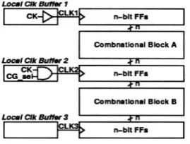
[image:2.595.363.498.232.334.2]These Synthesis-based clock gating is the most widely used method in EDA tools [6]. For example let a particular register stage is not active for a long time, the macro-including a local clock buffer, a register, and a combinational block - should be turned off by using a clock gating function as shown in Fig. 2.
Fig. 2 Transition in inverter input leading to switching power
This method is used in RTL data path to reduce the power consumption. In Fig. 2, a local clock buffer 1 is not clock-gated and always applies clock signal, CLK1 to n-bit register. The local clock buffer 2 is clock-gated, and if CG_sel signal is „0‟, then CLK2 is disabled. Hence, the power consumption due to CLK2 distribution and n-bit register can be ignored. And also, dynamic power consumption of the combinational block B, following the clock-gated register is also saved when the CLK2 is disabled. To precisely control enable signals for clock gating at each register stage can be used.
In auto gating flip flops, the frequency or period constraints at each stage are accepted from requirements and based on that the clocks are disabled for identified blocks [7].
There are several different types of the clock gating which are discussed here. Clock gating (CG) is the most popular, widely used and effective technique at RTL. For Register transfer level, digital circuits always contain some computations which are redundant, in other words, power reduction can be achieved by switching off these idle circuit operations [8]. Two typical non-CG circuits are mentioned in [9] as shown in Fig. 3(a) is the circuit without enable signal while the other one is with enable signal
Fig. 3 Non Clock gating circuit (a) Without enable (b) With enable
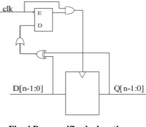
[image:2.595.328.543.615.694.2][12] techniques. These techniques reduce the power consumption by taking switching activity of signals into account. With the enable signal as shown in Fig. 3(b), includes local-explicit clock gating (LECG) [9], enhanced clock gating (ECG) [9], waste-toggle-rate-based (WTR) clock gating [9] and the single comparator-based clock gating (SCCG) [13] techniques. Bus-specific clock gating (BSC) is as shown in Fig. 4 is proposed in [10] for individual flip-flop (FF). The input and output bits are compared by XOR gates, when the input data are equal to the current output data, the XOR output is 0 and so does the output of N-bit OR gate which is used for determining the bit changes if any occur. So the FF is gated, the power has been saved.
Fig. 4 Bus specific clock gating
In Enhanced clock gating (ECG) as shown in Fig. 5, combines the gating circuits in BSC and LECG so that the clock signal of the register is gated as long as its toggle is waste [9]. Besides the advantages incurred by the low en signal in a significant percentage of the clock periods or the low signal switching activity, this gating circuit which is more complex than LECG incurs more power consumption when the situations aforementioned do not emerge.
Fig. 5 Enhanced clock gating
Threshold-based clock gating (TCG) when compared with BSC technique, which gates all the FFs without considering signal activities, in [11], Alberrto et al. has proposed this data-driven clock gating technique to improve BSC. In this technique, they claimed a threshold which is 5% of output switching activity, which means any FF whose output toggle rate is less than 5% need to be clustered and gated using one clock gating cell. The toggle rates of FFs of non-clock gating circuit need to be tested at first time, and then according to the list of toggle rate, those FFs are divided into two parts.
Optimized bus-specific clock gating (OBSC) in [12], Li et al. proposes a fine-grained activity-driven CG methodology which has improved BSC as well. Unlike TCG, this technique determines which FFs should be clustered and gated by taking the relationship of each and every FF into account [12]. The larger the FF output toggle is, the less the clock cycles are wasted, so the earlier that the FF should be excluded from gating [12].However, according to the much complex and
densities of the VLSI circuit, its drawback is obvious, this process takes too much time (e.g. for s15850, one sequential circuit of ISCAS‟89 benchmark, this time will be 28 hours).
Single comparator-based clock gating (SCCG) in [13], Wei et al. proposes a novel single comparator-based clock gating (SCCG) scheme to enhance the ECG for pipeline technique. In the proposed SCCG, enable signal has been moved from data path to control logic, the data signal is analyzed, and only single comparator is used to implement the clock-gating for all available pipeline stages.
The clock gating in the context of computing systems such as microprocessors must be distinguished from data paths of signal processing algorithms. The circuits implementing signal processing algorithms has higher scope of usage of clock gating based power optimization which is presented in detail in next section.
But the clock gating has also drawback of effecting clock‟s skew. Hence usage of clock gating has tradeoff between power consumption for performance. The proposed method with very less critical path delay for the clock gating enable logic, doesn‟t impose restrictions on performance. Details are presented in section IV.
3.
PROPOSED CLOCK GATING
ARCHITECTURE
As discussed in previous section, among several available clock gating techniques only few are suitable for signal processing applications on FPGAs. The work presented at [3] proposes Look-Ahead Clock Gating (LACG). It computes the clock enabling signals of each FF one cycle ahead of time, based on the present cycle data of those FFs on which it depends. The presented work here uses similar approach in addition to subword approach
A new architecture is proposed in this paper, whose key principle is detecting the presence of the information in the magnitude bits in a particular sub word out of a given word. In this method the n+1 bit width bus carrying a signal is considered, which uses 2‟s complement representation. The n bit magnitude word is divided into p subwords, each representing a particular part in the full dynamic range of signal. The Fig. 6, shows the sub word representation of the n+1 bit signal, where each sub word has m=(n/p) bits.
Fig. 6 (n+1) bit register represented as subwords
To generate the enable for clock gating, the presence of information is checked in each subword. The signal X represented with n+1 bits can be described as in (3). The subword based representation of same signal is given in (4).
(3)
XS= bn , bm−1 … . . b0 p−1, . . bm−1 … . . b01, bm−1 … . . b0 0
(4)
[image:3.595.108.233.449.552.2]high significant jth (i+1 < j < p-1) subwords has NIO flag „1‟. The no information flag at ith stage can be computing by using the OR gate in case of positive signals and NAND gate for negative numbers. In case of signal changing from negative to positive and vice versa the NOI flag must be set to zero. Considering these conditions the Fig. 4, implements the required enable signal generation for proposed clock gating scheme. The inverse of NOI flag will be used as enable for clock signal. The Fig. 4, has the logic for generating the enable for clock of ith subword. Since the 0th sub-word consist the least significant bits in the signal, it will always contain information even for smaller magnitude of the data in the register, except only in case when signal is zero. Implementing information detection clock gating enable generation logic for the LSB sub word will be an overhead. So in this paper the clock gating enable generation logic is implemented only for p-1 sub-words. In the present implementation each sub-word is enabled by logic ENi. The figure below illustrates the optimal circuit/logic for implementing the enable logic for ith stage sub-word.
[image:4.595.74.271.282.609.2]Fig. 7 ENi generation for ith subword
Fig.8 Pipe-lined Adder/Multiplier with sub-word based enable generation logic
The area overhead resulting due to the enable generation logic is certainly needed is considered while performing end to end power optimization analysis. Having selected the architecture for implementing the signal processing algorithm it is suitable for the proposed scheme to select an architecture where a single signal is streamed to multiple combinational signals. The Fig. 8 shows the implemented clock gating logic on two registers each with 3 subwords. The outputs of two registers are given to combinational logic as shown in figure. This subword based clock gating enabled registers will be used in next section to implement pipelined FIR filter.
4.
TRANSPOSED FIR FILTER
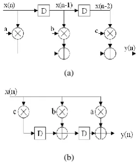
In this paper FIR filter architecture is selected to demonstrate the proposed clock gating scheme. The choice of FIR filter is due to its wide usage in implementing of many signal processing algorithms. Also several other signal processing operations like Fourier transform and correlations use multiply and accumulate operation, which is same as FIR filtering. Hence the FIR filter is selected for implementing the clock gating scheme. The Fig. 9(a) shows normal form of FIR filter implementation and Fig. 9(b) shows the transposed form of the same FIR filter implementation. The transposed architecture is suitable [14] for high speed implementation.
(a)
(b)
Fig. 9 FIR filter architecture (a) Direct form (b) Transposed form with pipelining
The transposed form of FIR filter implementation employs pipelining technique by inserting the registers in adder path. In the pipelined based FIR filter the input X is common to all the N multipliers and since it is common the enable generation logic is being optimized and it is relatively against N enable generation circuits only one enable logic will be used. Hence the increased overhead due to enable generation logic is less with this proposed architecture. The register shown in Fig. 8 is used to in implementing the transposed FIR filter. The total design is is coded using VHDL with generic coding style such that the number of subwords and accordingly bits in each subword can be changed. The simulation results and power analysis are given in next section.
5.
SIMULATION AND POWER
ANALYSIS
The subword clock gating enabled register is simulated to verify the basic principles of disabling the subword sections when there is no information in them. The input is taken from Direct Digital Synthesis (SINE wave) such that over different amplitude levels the enabling or disabling of subwords can be analyzed. The Fig. 10 has simulation results.
[image:4.595.319.557.643.737.2]Further to the register level verification of clock gating and ensuring that the basic functionality is not disturbed the top level FIR module is simulated with VHDL test benches. The test bench consists of SINE wave source plus additive white Gassian noise. The Fig. 11 has simulation results.
Fig. 11 Simulation results of FIR filter
The simulation is performed for input signal with SINE wave which falls in pass band of filter. Hence the output contains the SINE wave component as it is. Whereas the input noise gets attenuated considerably because the noise which is present at stop band is attenuated by the filter. The functional validation of filter proves that the clock gating and subword level partitioning of register are not affecting the main functionality.
[image:5.595.317.543.72.189.2]Using Xilinx Power Estimator (XPE) the power analysis has been carried out. The synthesized files for Virtex-6 Lx240 FPGA are used for timing simulation and further for generating the (Value chain dump) VCD files. These files consists all the transitions in the signals of both combinational and sequential logic. This method of power estimation is more suitable for the proposed technique as the number of input switching activities over a given period of time, averaged power analysis is more suited. The tool generated results for case without subword based clock gating is given at Fig. 12. The dynamic power 21 mW is considered here for analysis. The IOs and leakage element is not considered for technology, as they are mainly dependent on the specific device being used.
Fig. 12 Xpower report for FIR architecture without clock gating
The Xpower report for architecture with proposed clock gating method is given in Fig. 13. The dynamic power consumed for clock gating based design is 11 mW, without considering the IOs associated power component.
Fig. 13 Xpower report for FIR architecture with proposed clock gating
[image:5.595.55.283.128.273.2] [image:5.595.307.552.297.476.2]The dynamic power dissipation components are considered here for comparison. The results show 21 mW in case of no clock gating and 11 mW for clock gating conditions. The table I, compares the two architectures. It can be observed that the area over head due to power gating is very minimum (only additional 8 LUTs and 4 registers) but the power saving is 47%.
TABLE. I Area, performance and power comparison
Table Column Head
Parameter
Without clock gating
With clock gating
1 Area - LUTs 166 174
2 Area - Registers 112 116
3 Area - DSP48 6 6
4 Maximum clock speed 156 MHz
156 MHz
5 Dynamic power 21 mW 11 mW
6.
CONCLUSIONS
A new method for sub-word based enable generation for clock gating is developed. The method is suitable for VLSI implementation of several different signal processing architectures. The Results demonstrate power saving of 47% with clock gating to transposed FIR filter compared to the same transposed FIR filter without clock gating. The Area, Speed and Power consumption are compared. The area overhead is negligible due the novel scheme proposed to detect the information in subwords. The Xilinx 45nm FPGA Virtex6 LX240 FPGA is used for analysis and implementation. Xilinx Vivado tools are used for accurate power analysis using timing simulation models. The work is part of ongoing research on power optimization techniques. It is aimed to be continued in the direction of further studying the suitability of this technique for different algorithms.
7.
REFERENCES
[1] Michael Keating, Robert Aitken, Kaijian Shi, David Flynn and Alan Gibbons, “Low Power Methodology Manual For System-on-Chip Design” , Springer science business media, e-ISBN 978-0-387-71819-4, 2007.
[2] V. G. Oklobdzija, Digital System Clocking – High-Performance and Low-Power Aspects. New York, NY, USA: Wiley, 2003
[image:5.595.56.282.530.688.2]I: Regular Papers, IEEE Transactions on , vol.61, no.5,
pp.1465,1472, May 2014
doi: 10.1109/TCSI.2013.2289404.
[4] D. Brooks, P. Bose, S. Schuster, H. Jacobson, P. Kudva, A. Buyuktosunoglu, V. Zyuban, M. Gupta, and P. Gook, “Power-aware micro architecture: design and modeling challenges for next-generation microprocessors,” in IEEE Micro, vol. 20, no. 6, pp. 26-44, Nov.-Dec. 2010.
[5] W. Shen, Y. Cai, X. Hong, and J. Hu, “Activity and register placement aware gated clock network design,” in Proc. ISPD, 2008, pp. 182–189.
[6] Synopsys Design Compiler, www.synopsys.com
[7] “FPGA-Based Prototyping Methodology Manual.” Synopsys, Inc. All rights reserved, 2011.
[8] M. Pedram and A. Abdollahi, Low-power RT-level synthesis techniques: a tutorial, Computers and Digital Techniques, IEE Proceedings, Volume 152, Issue 3, Page(s):333 ̢ 343, 6 May 2005.
[9] L. Li and K. Choi, Selective clock gating by using wasting toggle rate, Electro/Information Technology, 2009. eit '09. IEEE International Conference, page(s): 399-404.
[10] T. Lang, E. Musoll, and J. Cortadella. Individual flip-flops with gated clocks for low power datapaths. IEEE TCAS-II: Analog and Digital Signal Processing, 44(6), 1997.
[11] A. Bonanno, A. Bocca, A. Macii, E. Macii., and M. Poncino. Data driven clock gating for digital filters. Integrated Circuit and System Design Power and Timing Modeling, Optimization and Simualtion.
[12] L. Li and K. Choi, Activity-driven optimized bus-specific-clock- Gating for ultra-low-power smart space applications, IET Commun., 2011, Vol. 5, Iss. 17, pp. 2501–2508.
[13] W. Wang, Y. C. Tsao, K. Choi, S. Park, M. K. Chung, Pipeline power reduction through single comparator-based clock gating, SoC Design Conference (ISOCC), 2009 International , page(s): 480-483.
[14] L. Aksoy, C. Lazzari, E. Costa, P. Flores, and J. Monteiro, “Design of digit-serial FIR filters: Algorithms, architectures, and a CAD tool,” IEEE Transactions on Very Large Scale Integration (VLSI) Systems, vol. 21, no.3,pp.498–511,Mar.2013.
8.
AUTHOR’S PROFILE
A. Ranganayakulu obtained his bachelor‟s degree from Nagarjuna University and Masters degree from JNT University. Areas of interest are VLSI Design, VHDL Programming, Digital system design, Low power VLSI design. He is having experience of 22 years in the field of teaching. Presently working as associate Professor of ECE Department, KITS, Markapur, A.P. INDIA.
K .Satya Prasad working as professor in ECE Department, JNTUK, Kakinada, India. He received his Ph.D from IIT, Madras. He has more than 33 years of experience in teaching and 25 years of R&D. He is an expert in Digital Signal Processing. He guided 14 Ph.D‟s and guiding 10 Ph.D Scholars. He authored Electronic Devices and Circuits, Network Analysis and Signals& systems text books. He held different positions in his carrier like Head of the Department, Vice Principal, Principal for JNTU Engineering College and Director of Evaluation & Rector of JNTUK. He published more than 100 technical papers in National and International Journals and Conferences.