PROGRAMMER'S REFERENCE MANUAL
FORAN
L-3055 DATA PROCESSING SYSTEM
USED AS THE
AN/FYQ-11 DATA PROCESSOR SET
15 September 1963
General Precision, Inc. Inforrna tion Sy sterns Group
LIST OF EFFECTIVE PAGES
Total number of pages in this publication is 318 consisting of the following:
Page No. Title
A
iii thru xvii 1- 0 thru 1 - 1 0 2 -1 thru 2 -14 3-1 thru 3-10 4-1 thru 4-57 5-1 thru 5-6 6-1 thru 6-29 7-1 thru 7-9 8-1 thru 8-37 9-1 thru 9-25 10-1 thru 10 - 1 5 11 -1 thru 11 -18 12-1 thru 12-21 13-1 thru 13-24 14-1
15-1 thru 15-5 A-I thru A-3
B-1 thru B-4 C-l thru C-6 D-l thru D-3 E-l thru E-3
-'- -,-Issue Original Original Original Original Original Original Original Original Original Original Original Original Original Original Original "-Original Original Original Original Original Original Original Original
TABLE OF CONTENTS
Section I INTRODUCTION
1. 1 SYSTEM FUNCTIONS . . 1. 2 SYSTEM FEATURES . 1. 3 CENTRAL PROCESSOR 1.4 CORE MEMORY.
1.5 DISC MEMORY
1.
6
REAL-TIME COMMUNICATION 1. 7 UNI-RECORD FACILITIES 1.8 CHECKING FEATURES 1. 9 DUPLEXING . . . . 1. 10 PROGRAM INTERRUPTSSection II CORE MEMORY AND WORK FORMAT 2. 1 MEMORY REGISTERS . .
2.1.1 Memory Address Register 2.1.2 Memory Access Register (M) 2.2 SPECIAL FEATURES . . . .
2. 2. 1 Cycle Demand Priority
2.2.2 Individual Memory Trunkline 2.2.3
2.2.4
Shared Memory Trunkline . . Module Address Patchboard 2.2.5 Core Memory Twinning. 2.3 INFORMATION FORMAT.
2.3.1 Word 2. 3.2 Character 2.3.3 Bit . . . .
2.3.4 Alphanumeric Data Word 2.3.5 Floating-Point Data Word 2.4 INSTRUCTION WORD FORMAT.
2.4.1 Command Character (C) 2.4.2 Select Characters (ZY) 2.4. 3 Index Character (X) . .
2.4.4 Memory Address Characters (MMMM)
Page 1 -1 1-5
1-6
1-6
1-7 1-7 1-8 1-81-9
1-9
2 -1 2 -1 2 -1 2-2 2-2 2-2 2 -2 2-3 2-5 2-5 2-52-6
2-6
2-7 2-8 2-9 2-10 2-10 2-11TABLE OF CONTENTS - Continued
Section II (Cont 'd)
2.4. 5 Zone Bit Options • . . . . • • . • . .
Section III CENTRAL PROCESSOR
3.1 ARITHMETIC SECTION ,
3.2
3.3
3.4
3.53. 1 • 1
R Register 3.1.2 A Register 3,1.3 Q Register 3. 1 .4 Toggle s ••• 3 • 1 • 5 Adde r • • •PROGRAM CONTROL SECTION. 3.2. 1 3.2.2 3.2.3 3.2.4 3.2.5 3.2.6 3.2.7 3.2.8 3.2.9
Instruction Addre ss Register (Ia) Operand Addre ss Register (Oa) .• Index Holder (Xh) . • • •
Command Holder (C) Z Holde r (Z) . • Y Holder (Y) . . X Counte r (X)
Index Modify Register (B) • Index Registers (Xrl-Xr17) • .
.
.
3.2.10 Toggles and Switches • • • • . •
PROGRAM CONTROL SEC TION OPERATION . .
3.3. 1
3.3.2 3.3. 3
MASM Operand Address Store Flagged Return Address
Indirect Addre s s • 3.3.4 PDPM Operation.
3. 3. 5 Index Modify • . • • • • • •
PUSH-DOWN POP-UP MEMORY MODE (PDPM) .• MULTI-ADDRESS STACKING MEMORY MODE (MASM)
Section IV INSTRUCTIONS
4.1 ARITHMETIC INSTRUCTIONS 4. 1 • 1
4. 1 .2
Add . . . . • • • .
Subtract . • • • •
TABLE OF CONTENTS - Continued Section IV (Cont'd)
4.2
4.3
4.4
4.5
4. 1 . 3
4. 1.4
4. 1. 54.1.6
Add A to M, Place in R • • • . • • . Subtract A from M, Place in R .• Multipl y Long .
Multiply Short. 4.1. 7 Divide Long 4. 1.8 Divide Short
DATA MOVE INSTRUCTIONS. 4.2. 1 Bring M to A • • • •
.
.
4.2.2 Com bine M with .A 4.2.3 HoldA to M4.2.4 Jerk M to R 4.2.5 Keep R to M 4.2.6 Load M in ZY .
4.2.7 Save ZY in M
. .
.
.
.
4.2.8 Copy Z to Y4.2.9 Left Shift.
4.2.
10 Right ShiftCOMPARE INSTRUCTIONS 4.3.1 Alphabetic Compare.
Numeric Compare ••
.
.
4.3.2 4.3.3 4.3.4
Field Compare, Automatic Shift. Index Register Compare
SET-CONVERT INSTRUCTIONS. 4.4.1
4.4.2 4.4.3 4.4.4 4.4.5
Set-Re set Toggle. Set-Re set Bit Logical OR . • • • Logical AND. Convert . • • • •
PROGRAM CONTROL INSTRUCTIONS. 4.5.1 No Operation • • • • • • • • 4.5.2 Unconditional Transfer.
TABLE OF CONTENTS - Continued Section IV (Cont'd)
4.5.3 Test • • • . . • • 4.5.4 Bit Compare •• 4.5.5
4.5.6 4.5.7
Execute . • • • •
Modify Index Re gi ste r •• Hal t . • • . • . • • . . • • • .
4.6 FLOA TING-POINT INSTRUCTIONS.
Page 4-38 4-39 4-40 4-40 4-41 4-41 4.6. 1 Floating-Point Add. • • • . • 4-43 4.6.2 Floating-Point Subtract. . • • • • • • • • • • • • •• 4-45 4.6. 3 Floating-Point Add A to M and place in R. • • • •• 4-48 4.6.4
4.6.5 4.6.6 4.6.7
Floating-Point Subtract A from M and Place in R Floating-Point Multiply Long . • . • • • • •
Floating-Point Divide Long . • • • • Floating-Point Numeric Compare.
Section V I/O INTERFACE
5.1 I/O BUFFER REGISTER . . 5.2 CHARACTER HOLDER 5. 3 SCANNER . . • • . . • • . . 5.4
5. 5 5.6
I/O INSTRUCTION REGISTER
I/O INSTRUCTION LOCATION REGISTER OUTPUT OPERATION
5.7 INPUT OPERATION . . . 5. 8 ERROR CONSIDERATION
5. 9 ST A TUS INDICA TORS AND DEVICE ADDRESSES 5.10 I/O INTERFACE INSTRUCTION FORMAT
5. 1 O. 1 In pu t . 5. 1 O. 2 Ou tpu t .
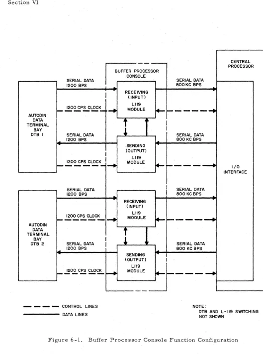
Section VI BUFFER PROCESSOR
6.1 BUFFER PROCESSOR CONFIGURATION. 6.2 INPUT MESSAGE TRANSFER . • . . . .
6. 2. 1 Data Link to Receiving L-11 9 •
6.2.2 Receiving L-119 to Central Processor.
TABLE OF CONTENTS - Continued
Section VI.,(Cont'd)
6.3 OUTPUT MESSAGE TRANSFER
6 .. 3.1 Central Processor to Sending L-119
6. 3. 2 Sending L-119 to Data Link
6.4 MESSAGE STORAGE • . . .
6.5 L-119 MODULE DESCRIPTION
6. 5. 1 Input/Output Interfac.e. .
6.5.2 Disc Memory • . . . • . .
6. 5. 3 Major Logical Elements
6.5.4 Buffer Processor Words . .
6.5.5 Memory Addresses . . . • .
6.5.6 Memo Assignments • • . • .
6. 6 BUFFER PROCESSOR INSTRUCTIONS
6. 7 INSTRUCTION SEQUENCING .
6.7. 1 Instruction Retrieval . .
6. 7. 2 Normal Instruction Timing . .
6. 7. 3 Me s sage Track Instruction Timing
6.7.4 Input Message Sequence . . . .
6. 7. 5 Output Me ssage . . . • . . . .
6.8 BUFFER PROCESSOR OPERATION . . . . •
6.8.1 Controls and Indicators . • . . •
6.8.2 Buffer Processor Operating Procedures
Section VII UNI-RECORD INTERFACE
Page 6-7 6-7 6-10 6-11 6-11 6-11 6-13 6-14 6-16 6-16 6-1 7 6-19 6-21 6-21 6-21 6-22 6-22 6-23 6-24 6-24 6-27
7. 1 UNI-RECORD BUFFER REGISTER. . 7-1
7. 2 CHARACTER HOLDER. . 7-1
7. 3 WORD COUNTER . . . 7-1
7.4 UNI-RECORD INSTRUCTION REGISTER. • 7-2
7.5 UNI-RECORD INSTRUCTION LOCATION REGISTER. . 7-2
7.6 STATUS AND ERROR TOGGLES. . . 7-2
7.7 UNI-RECORD DEVICE ADDRESSING 7-5
7.8 UNI-RECORD INTERFACE INSTRUCTIONS.. 7-5
7 . 8. 1 Inpu t . 7 - 6
TABLE OF CONTENTS - Continued Section VII {Cont'd}
7.8.3 Test
7.9 TAPE TRANSPORT CONTROL INSTRUCTIONS 7. 9. 1 Backspace Tape -( . • • .
7. 9. 2 Forward-Space Tape -) 7.
9.
3 Rewind Tape - [ • . . . 7. 9.4 Write File Mark - --,Section VIII UNI-RECORD CONSOLES 8.1 TAPE TRANSPORTS . . . . • . . • . . •
8.1.1 Tape Transport On-Line Read 8.1. 2 Tape Transport On-Line Write . .
8.1.3 Tape Transport Mode Change Operation 8.1.4 Tape Transport Control Operations 8. 1. 5 Tape Transport Off -Line Operations 8.1. 6 Tape Transport Operation . . . . 8.1.7 Tape Transport Operating Procedures. 8. 2 CARD READER/PUNCH . . .
8. 2. 1 Console De scription. 8. 2. 2 Card Reader
8.2.3 Card Punch. 8. 3 LINE PRINTER . . . .
8. 3. 1 Line Printer On-Line 8.3.2 Line Printer Off-Line . .
Section IX DISC MEMORY
9.1 ORGANIZATION OF DATA 9. 1 . 1 Character . .
9. 1 . 2 Block . . . 9.1.3 Data-Band 9.1.4 Twin . . . 9.1. 5 Flag Tracks
Page 7-8 7-8 7-8 7-8 7-9 7-9 8-2 8-3 8-5 8-6 8-7 8-8 8-9 8 -12 8-16 8 -16
8 -1 7
TABLE OF CONTENTS - Continued
Se ction IX (Cont I d) Page
9.2 DISC MEMORY INSTRUCTION FORMAT .• 9-5
9.2.1 The Interface Construction Word . . 9-5
9.2.2 Disc Memory Operation Word . . . . 9-6 9.2.3 Key/Data Address and Mask-Control Address
Word. . . • . 9-6
9.2.4 Key Format . . . 9-7
9. 2. 5 Ma sk and Control Format
9.3 DISC MEMORY COMPONENTS
9.3.1 Disc Storage . . . .
9.3.2 Core Buffer and Search Registers . .
9.3.3 Disc Memory Operation Register
9.3.4 MC Buffer Store
9.3. 5 CP Buffer Store
9.4 DISC MEMORY INTERFACE .•
9. 4. 1 Inte rface Instruction Re gister
9. 4. 2 Interface Instruction Location Register
9.4.3 Interface Address Processing Register
9.4.4 Disc Memory Interface Operation.
9.5 DISC MEMORY OPERATION . .
9. 5. 1 Write Function
9.5. 2 Read Function.
9.5.3 Obsolete Function 9. 5. 4 Count Function . .
9.5. 5 Fixed Addres s Access
9.5.6 Obsolete Access
9.5.7 Content Access . .
9.5.8 Compare Flag Access
9.5.9 Multi-Block, First Qualify Access
9.6 TWIN MODE . . . .
9.7 STATUS TOGGLES
9.7.1 Overload . .
9.7.2 Twin Com.pare (ZY=/S)
TABLE OF CONTENTS - Continued
Section IX (Contt d) Page
9.7.3 9.7.4
Operative (ZY=/U) . . . . Display Backup (ZY=34) . 9. 7. 5 Interface Busy (ZY=3#)
9.7.6 Disc Memory Unit Busy (ZY=37) 9.8 WRITE INHIBIT SWITCHES . . . .
9-23 9-23 9-23 9-23 9-25
Section X DISC MEMORY OPERATIONS
10.1 FIXED ADDRESS OPERATIONS 10.1.1 Fixed Address Read. 10. 1. 2 Fixed Addres s Obsolete
10.1.3 Fixed Address Read and Obsolete 10. 1.4 Fixed Addres s Write . . . . 10.2 NON-FIXED ADDRESS INDIVIDUAL BLOCK
OPERATIONS . . . , . . . . .
10.2. 1 Content Acces s Read . . . . 10. 2.2 Content Acces s Read and Obsolete 10.2.3 Content Access Obsolete and Count 10. 2.4 Content Acces s Count.
10.2.5 Compare Flag Read
10.2.6 Compare Flag Read and Obsolete. 10.2.7 Obsolete Flag Write . . . . 10.3 NON-FIXED ADDRESS MULTI-BLOCK OPERATIONS . . . .
10-2 10 -2 10-3 10-3 10-4 10-4 10-4 10-5 10-5 10-6 10-6 10-7 10-7 10-8 10.3.1 10.3.2 10.3.3 10.3.4
Content Access Read Multi-Block. . 10-8 Content Access Obsolete Multi-Block 10-8 Content Access Read and Obsolete Multi-Block . . 10-9 Compare Flag Read Multi-Block . . . 10-9 10.3.5 Compare Flag Read and Obsolete Multi-Block
10.3. 6 Obsolete Flag Write Multi-Block 10.4 DISPLAY BUFFER WRITE OPERATIONS
10.4.1 Me Buffer Write . . . .
TABLE OF CONTENTS - Continued
Section X (Cont'd)
10.4.2 CP Buffer Write
10.5 PREPARE OPERATIONS
10.5.1 Select Disc Memory Module
10.5.'2 Load Key, Mask and Control . .
10.6 RET;URN OPERATIONS . . . .
10.6.1 Return Disc Memory Operation
10.6.2 Return Key, Mask and Control Information
10.6.3 Return Display Buffer Status . . . .
Section XI PROGRAM INTERRUPTS
11. 1
11. 2
11. 3
11. 4
11. 5
11.
6
11. 7INTERRUPT HIERARCHY . . . .
IGNORE INTERRUPT TOGGLES
INTERRUPT OPERATION . . .
INTERRUPT PROGRAM SELECTION
INTERRUPT PROGRAM EXIT . . . .
FLAGGED RETURN ADDRESSES . . . .
INTERRUPT CLASS: I/O INTERFACE (ZY=42)
11. 7. 1 Detail: Interface Not Busy (ZY=39) . .
11. 7.2 Detail: L-119 Mes sage Available (ZY=2, )
11.7. 3 Detail: Display Console Message Available (ZY=2#) . . . .
11. 7.4 Detail: Sending L-II9 Available (Z Y=2()
11.8 INTERRUPT CLASS: REAL-TIME (ZY=43) .
11.8.1 Detail: Real-Time Clock (ZY=3() .
11. 8.2 Detail: Interval Timer (ZY=3,) . .
11. 9 INTERRUPT CLASS (AND DETAIL): OTHER PROCESSOR (ZY=44) . . . .
11. 10 INTERRUPT CLASS: DISC MEMORY INTERFACE
Page 10-11 10-11 10-11 10-12 10-12 10-12 10-13 10-13 11 -1 11-2 11-2 11-3 11-4 11-4 11-4 11-4 11-5 11-5 11-5 11-5 11-5 11-5 11-5
(ZY=3[) . . . . . . 11-5
11.10.1 Detail: Interface Not Busy (ZY=2Y) . . . 11-6
11. 10.2 Detail: Dis c Memory Unit Not Busy (ZY=2Z) 11-6
TABLE OF CONTENTS - Continued
Section XI (Cont' d) Page
11. 11 INTERRUPT CLASS: UNI-RECORb INTERFACE
(ZY=3W) . . . . 11-6 11.11.1 Detail: Interface Not Busy (ZY=3Y). . . 11-6 11.11. 2 Detail: Operator (ZY=3Z) . . . 11-6 11. 12 INTERRUPT CLASS: ERROR (ZY=41) -(COMPUTER,
DATA TRANSFER) . . . 11-6 11.12.1 Detail: M Register Parity Error:
(ZY=Vl) . . . . 11-7
11.12.2 Detail: R Register (ZY=V2) 11-7
11.12.3 Detail: A Register (ZY=V3) 11-7
11.12.4 Detail: Q Register (ZY=V4) 11-7
11.12. S Detail: Arithmetic (ZY=VS) . . 11-7 11.12.6 Detail: R Repeater (ZY=V6) . 11-7 11.13 INTERRUPT CLASS: ERROR (ZY=41) -(COMPUTER,
ARITHMETIC) . . . 11-7 11. 13. 1 Detail: Overflow (ZY=Wl) . . .
11.13.2 Detail: F. P. Overflow (ZY=W2) . 11. 13. 3 Detail: Numerical (Z Y=W3) . . . . 11. 13.4 Detail: Convert Overflow (ZY=W4)
11.14 INTERRUPT CLASS: ERROR (ZY=41) -(COMPUTER, PROGRAM) . . . .
11.14.1 Detail: Instruction (ZY=Xl) . . . . 11.14.2 Detail: Illegal Address (ZY=X2) . 11.14.3 Detail: End of Memory (ZY=X3)
11.-lS INTERRUPT CLASS: Error (ZY=41) - INTERFACE, DISC MEMORY) . . . .
11.1S.1 Detail: Vertical Parity Interval
(ZY=/ 1)
..
11.1S.2 Detail: Horizontal Check Interval (ZY=/2)
11.1S.3 Detail: Flag Parity (ZY=/3). 11.IS.4 Detail: Fixed Address (ZY=/4) 11.1S.S Detail: M Register (ZY=/S) 11.1S.6 Detail: Write (ZY=/6).
TABLE OF CONTENTS - Continued Section XI (Cont'd)
11. 15. 7 Detail: Instruction (Z Y= /7) . . . . 11.15.8 Detail: Hang Up (ZY=/8) . . . . 11. 15.9 Detail: Transmission Parity (ZY=/9) 11.15.10 Detail: Out of Temperature (ZY=/=) 11.15.11 Detail: Slow Down (ZY=/ ') . . . 11.15.12 Detail: Operand Address (ZY=/» 11.15.13 Detail: Count (ZY=36) . . . 11. 16 INTERRUPT CLASS: ERROR (ZY=41)
-(INTERFACE, I/O) . . . . 11.16.1 Detai1: Parity (ZY=Sl) . . . . . 11. 16.2 Detail: M Register (ZY=S2) . 11. 1 6. 3 Det ail: Hang Up (Z Y =S 3) . . . .
11.16.4 Detail: Operand Address (ZY=S4) . .
11.17 INTERRUPT CLASS: ERROR (ZY=41) - (INTERFACE, UNI-RECORD) . . . .
11.17.1 Detail: On Line Data (ZY=Tl)
...
11.17.2 Detail: On Line Evesdrop (ZY=T2)...
11.17.3 Detail: On Line Mechanical (ZY=T3) 11.17.4 Detail: M Register Parity Error (ZY=T4) 11.17.5 Detail: Horizontal Check (ZY=T5) .11.17.6 Detail: Instruction (ZY=T6) .
....
11.17.7 Detail: Overload (Z Y=T7) . . . 11.17.8 Detail: Real World Parity (ZY=T8) 11.17.9 Detail: Real World Mechanical (ZY=T9) 11.17.10 Detail: Device Unavailable (ZY=T» 11.17.11 Detail: Operand Addres s (ZY=T <)Section XII DUPLEXING
12.1 BUFFER PROCESSOR SWITCHING 12. 1. 1
12.1.2 12.1. 3
Receiving L-119 Module Controls Sending L-119 Module Controls
L-119 Module Pair Controls . . .
TABLE OF CONTENTS - Continued Section XII (Cont'd)
12. 1.4 Receiving L-119 Module Indicators 12. 1.5
12. 1.6 12. 1.7 12.1.8 12.1.9
Sending L-119 Module Indicators
Testable L-119 Module Control Switches L-119 Module Operation from the Central Switching Console
Audible Alarm . . . . . . Test Indicators Button 12.2 AUTODIN REMOTE CONTROLS
12. 3
12.2. 1 Sending Crypto Controls 12.2.2 Receiving Crypto Controls
12.2. 3 Control Switch and Indicator Power. 12.2.4 Operation of Autodin Controls . . . . INTEGRATED CONSOLE SWITCHING . . . . 12. 3. 1 Electronic Typewriter Switching . . 12. 3.2 Display and Console Printer Switching 12.4 DISC MEMORY TRUNKLINE
12.4. 1 Control Status Toggle
12.4. 2 Dis c Memory Trunkline Coupling Mode Toggle . . . .
12.4.3 Other Disc Memory Busy
Section XIII CONTROL CONSOLE AND CENTRAL PROCESSOR CONTROL PANEL 13.1 CONTROL CONSOLE CONTROL PANEL 13.2 CONTROL TYPEWRITER.
13.2. 1 Manual Input . . . 13. 2.2 Typewriter Instructions
13.3 CENTRAL PROCESSOR CONTROL PANEL 13. 3. 1 Left Section Indicators
13. 3.2 Center Section Indicators
13. 3. 3 Right Section Controls and Indicators
Page 12-5 12-6 12-7 12-8 12-9 12-10 12-10 12-10 12-11 12-11 12-11 12-13 12-13 12-14 12-20 12-20 12-20 12-20
Section XIV
TABLE OF CONTENTS - Continued
REAL-DASH TIME CLOCK AND INTER VAL TIMER
14. 1 REAL-DASH TIME CLOCK
14.2 INTERVAL TIMER . . . .
Section XV DISPLAY CONSOLES
15.1 ELECTRONIC TYPEWRITER ET
15. I. I Input Messages . . . .
15.1.2 Output Messages . . . . .
15.2 LOGIC KEYBOARD ASSEMBLY LKB
15. 3 MULTI COLOR DISPLAY MC
15.4 CONSOLE PRINTER CP . . .
15.5 HARDCOPY ASSEMBLY HC .
Page
14-1
14-1
15-2
15-2
15-3
15-4
15-4
15-5
ILL USTRA TIONS
Data Processor Set AN/FYQ-l1 Figure
1-1
1- 2 AN /FYQ-Il Data Flow and Switching Control Diagram. 2-1 Memory Address Selection Patchboard
2- 2 Information Word Format 2-3 Instruction Word Format . .
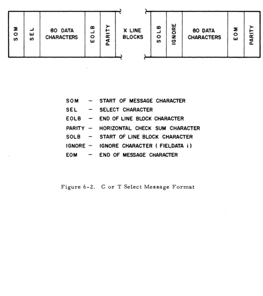
6-1 Buffer Processor Console Functional Configuration 6- 2 C or T Select Me s sage Format
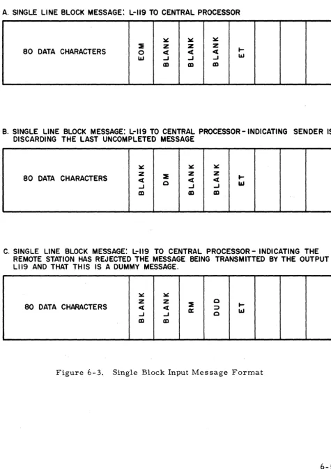
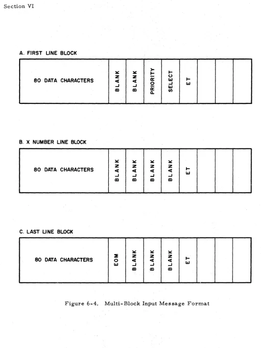
6-3 Single Block Input Message Format 6-4 Multi-Block Input Message Format.
6-
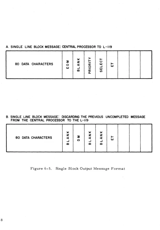
5 Single Block Output Message Format . . 6-6 Multi-Block Output Message Format 6-7 L-119 Block Diagram . . . .6-8 7-1 8-1 8-2 8-3 8-4 9-1 9-2
Buffer Processor Maintenance Panel Uni-Record Device ZY Addresses . . . Magnetic Tape Console Control Panel Card Flow Diagram . . . . Card Reader /Punch Control Panel Line Printer Control Panel . . . . Index-Data-Fixed Address-Flag Format Content A.cces s - Example.
Display Buffer Status Word Interrupt Hierarchy . . . System Switching Configuration
...
Page 1-0 1-3 2-4 2-6 2-10 6-2 6-3 6-5 6-6 6-8 6-9 6-12 6-26 7-5 8-10 8-18 8-25 8-35 9-3 9-21 10-15 11-19 12-2 10-1 11-1 12-1Figure 12-3 12-4 12-5 13-1 13-2 13-3 13-4
E-1
ILL USTRA TIONS - Continued
Central Switching Console Control Panel, Right Section
Page 12-16 Central Switching Console Control Panel, Left Section . . . 12 -1 7
Switching Status Work (ZY 17) . . 12-19
Control Console Control Panel
Central Proce s sor Control Panel, Left Section. Central Proces sor Control Panel, Center Section Central Processor Control Panel, Right Section Central Processor Functional Block Diagram . .
· 13-2 . . 13-8 · 13-15 · 13-22
CONTROL-INDICATOR CONSOLE OA- 6041/FYQ-11
LlARY MAGNETIC TAPE
~ L-3556 DISC ::::-- ______ MEMORY GROUP ______ OA-458I/FYQ-11
ELECTRIC TYPEWRITER AND CONTROL KEYBOARDS
---INPUT MAGNETIC TAPE OA - 4590/FYQ -II
DATA PROCESSOR
GROUP OA-4580/FYQ-11
CARD READER
PUNCH L-3575
~
OPERATIONS CENTER
DATA PROCESSOR SET CONTROL
CONSOLE OA-4654/FYQ-1I
Section I
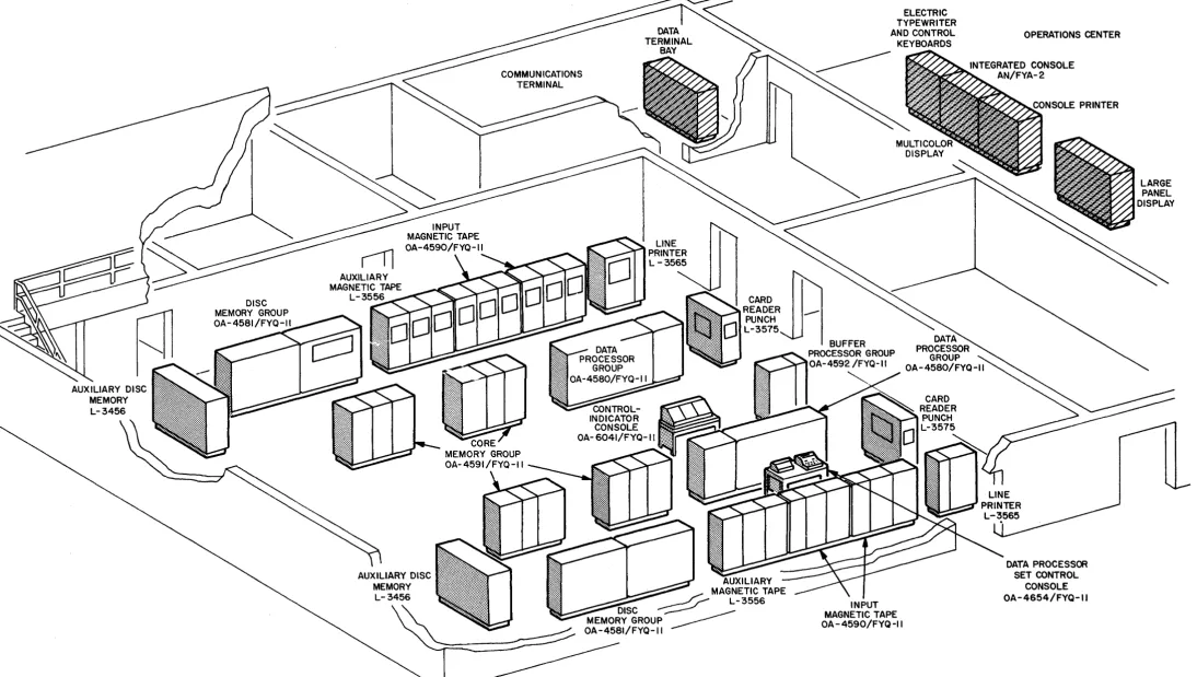
[image:20.1227.96.1190.70.689.2]SECTION I
INTRODUCTION
Section I Paragraph 1. 1
This publication is the Programmers Reference Manual for an L-3055 Data
Proc-essing System used as the Data Processor Set AN/FYQ-ll, figure 1-1, a
sub-system of the 473L Command and Control System. Content of the manual is
orien-tated around system functional information that is needed for programming. This
manual consists of 15 sections that are bound in one volume.
The system described is the Complete Operating Capability (COC) for Data
Processor Set AN/FYQ-ll. The Dat"a Processing System operates with the
Inte-grated Console Subsystem, Large Panel Display Subsystem and Data
Communica-tions Subsystem (AUTODIN) to provide large scale automatic processing, display
and transmission of information. On-line and off-line magnetic tape, card reader/
punch, and line printer operations are provided by the system.
1. 1 SYSTEM FUNCTIONS.
The Data Processing System consists of on-line, real-time general purpose
alphanumeric data processing equipment that performs arithmetic, logical, storage,
control, and retrieval operations on various inputs and stored data to produce
out-puts under program, operator, and automatic control. This data processing
equipment maintains control of data by acquisition, filing, distribution,
transmis-sion, and monitoring.
The Data Processing System provides for inputs through digital data links,
inte-grated console typewriters, a control console, a card reader, and magnetic tapes.
Outputs are provided through integrated console typewriters, integrated console
printer, integrated console displays, large panel displays, line printer, control
console typewriter, card punch, magnetic tapes, and digital data links.
The basic functions of input-output, data processing and storage are performed by
the four major elements of the system:
a. Central Processor, Control Console, and Core Memory.
b. Buffer Processors for real-time inputs from digital data links, and outputs
Section I
Paragraph 1. 1
Co Uni-Record devices consisting of Magnetic Tape Consoles, Card Reader/
Punch, and Line Printer.
d. Disc Memory for fixed address or content-access operations and integrated
console buffer storage.
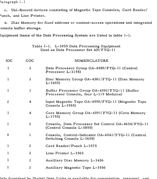
Equipment items of the Data Processing System are listed in table 1-1.
IOC 1 1 1 2 1 1
o
1 1 1 1Table 1-1. L-3055 Data Processing Equipment Used as Data Processor Set AN/FYQ-ll
COC NOMENCLATURE
2 2 1 4 4 2 1 2 2 2 2
Data Processor Group OA-4580/ FYQ-Il (Central Processor L-3155)
Disc Memory Group OA-4581/FYQ-l1 (Disc Memory L-3455)
,
Buffer Processor Group OA-4592/FYQ-ll (Buffer Processor Console, four L-I19 Modules)
Input Magnetic Tape OA-4590/ FYQ-l1 (Magnetic Tape Console L-3555)
Core Memory Group OA-4591/FYQ-Il (Core Memory L-3755)
Console, Data Processor Set Control OA-4654/ FYQ-ll (Control Console L-3855)
Console, Control-Indicator OA- 6041 / FYQ .. 11 (Central Switching Console L-3655)
Card Reader/Punch L-3575
Line Printer L-3565
Auxiliary Disc Memory L-3456
Auxiliary Magnetic Tape L-3556
Data furnished by Digital Data Links is available for computation, retrieval, and
display under automatic control of stored programs and upon manual request. The
system performs computations on the data, arranges the format, updates stored
[image:22.620.58.574.43.632.2]AUXILIARY DISC MEMORY L-3456 AUXILIARY DISC MEMORY L-3456
..
-.
-DISC MEMORY GROUP OA- 4581/FYQ-11
CORE MEMORY GROUP
OA-459I/FYQ-11
t
CORE MEMORY GROUP
OA-4591/FYQ -II
AUXILIARY MAGNETIC TAPE L-3556
INPUT
MAGNETIC TAPE OA-4590/FYQ-11
INPUT
MAGNETIC TAPE OA-4590/FYQ -II LINE PRINTER L-3565
I
Section II
I
r
.~
t
IINTEGRATED CONSOLE
I
AN/FYA-21
LARGE PANEL DISPLAY
I
~---~DATA PROCESSOR SET CONTROL CONSOLE
I
I
I
I
" " , Ir OA-4654/FYQ-1I "
1
I
CORE MEMORY GROUP
OA - 4591/FYQ -II
DATA PROCESSOR GROUP OA - 4580/FYQ-1I
1
.
-
r -CARD READER/ PUNCH L-3575 -ELECTRIC TYPEWRITER AND CONTROL KEYBOARDS MULTI-COLOR DISPLAY CONSOLE PRINTEROPERATIONS CENTER
...
- - - - -
---
-CONTROL- BUFFER AUTODIN DATA.... .... AUTODIN
INDICATOR
~ ~
-II PROCESSOR GROUPI-III!t---...I--~~
TERMINAL BAY M_t----P_ COMMUNICATIONSL ______ _
~---.
CONSOLE OA-4592/FYQ-1I 763.2A
r - --- - - - -
I- - - - -~O_A_-6_0r4_I/_F-:YrQ_-_"_ I .I
;
t ___________
.~---.J
I
CORE MEMORYD~TA
PRO:ESSOR GROUPI
GROUP~~
OA-4580/FYQ-1II
OA - 4591/FYQ - IICOMMUNICATIONS TERMINAL
DATA FLOW
I
I
DATA PROCESSOR SET CONTROL CONSOLE
CARD READER/ PUNCH
L-3575
---SWITCHING CONTROL AND REMOTE INDICATORS
I
OA -4654/FYQ -IIl
,~
l
DISC MEMORY GROUP OA - 4581 /FYQ-II
AUXILIARY MAGNETIC TAPE L-3556
INPUT
MAGNETIC TAPE OA-4590/FYQ-11
INPUT
MAGNETIC TAPE OA-4590/FYQ ~ II
LINE PRINTER L-3565
[image:23.1227.79.1177.76.665.2]Section I Paragraph 1. 2 Digital Data Links. Program s control the execution of the functions required for the operational tasks. A control program supervises the reception of messages which are to be decoded and processed for transmission or display.
Rapid processing and retrieval of a wide variety of information as well as the execution of specific programs requires close interaction between manpower and the system. Considerable scheduling and system control is necessary to establish priorities, eliminate unnecessary delays, and perform the processing operations on a dynamic real-time basis. Characteristics of the units, the data peripheral devices, and programming must be understood by personnel responsible for the programming and operation.
The Data Processing System communicates electronically with units of the system and peripheral equipment by means of trunklines, buffers, and interfaces, fig-ure 1- 2. The Disc Memory Trunkline provides for communication between the Central Processor and Disc Memoryo The Uni-Record Trunkline provides for data transfer and control between the Central Processor and the Magnetic Tape Console. The Tape Transports, Line Printer, Card Punch, and the Card Reader are the Uni-Record devices which are addressed by appropriate input or output instructions. The I/O Interface provides for data transfer between the Buffer Processor or an Integrated Console Electronic Typewriter, and the Central Processor. The I/O Interface in the Central Processor selects the particular Buffer Processor Module or Integrated Console Typewriter, and designates the operation to be performed.
1. 2 SYSTEM FEATURES.
The Central Processor operates in parallel on words of eight alphanumeric characters. The magnetic Core Memory is modularly expandable up to 64, 000 words. The Disc Memory, utilizing large discs, offers both fixed address and
content access. The real-time interface provides time shared memory operation, as well as buffering, and separately programmed data-link operation. A Uni-Record Trunkline handles magnetic tapes, punched card equipment and a line printer.
All data transfers are parity checked, with provision for programmed error re-covery. Multiplexing of all major system elements permits maintenance with reduction, but not loss, of capability.
Section I
Paragraphs 1. 3 to 1. 4
The entire Data Processing System has been organized to provide ease of
program-ming, speed of operation, reliability, and general purpose flexibility.
1.3 CENTRAL PROCESSOR.
The Central Processor has an alphanumeric character organization with decimal
memory addressing. The computer word of eight. characters provides variable
field flexibility with fixed word simplicity. Single address instructions specify a
required field within any memory or register word for most operations.
There are 43 basic commands, including input and output. Control characters and
flags within the instruction word extend the range of program operations.
Auto-matic index modification is provided with all commands that specify an operand or
next-instruction address. Two Index registers are static and 15 more are in the
Core Memory. Indirect addressing and indirect instruction execution, with index
modification, is provided.
The Central Processor may use the Core Memory in either of two special modes,
PDPM (Push-Down, Pop- Up Memory), and MASM (Multi-Address Stacking Mode).
Programmed memory comparisons may range over regions of Core Memory word
by word, or on a character field basis, independent of word boundaries.
The Central Processor operates at a clock frequency of 1. 5 megacycles. Data transfers with the Core Memory are full-word parallel, while most other
opera-tions between registers (including addition) are in half-word parallel. Typical
operation times including instruction and operand access are: addition (non-indexed)
10. 5 microseconds; full word multiplication 25. 0 microseconds; indexing, an
additional 20 0 microseconds (static); 5. 0 microseconds (from core).
1. 4 CORE MEMORY.
The five-microsecond cycle time magnetic Core Memory is provided in modules of
4000 words of 56 bits each. Module addres ses are patched in the Central
Proces-sor. Each Central Processor may address 64, 000 words of memory, of which
32,000 words can be shared between two Central Processors.
A special twinning feature allows duplicate writing in a pair of individual
(non-shared) memory modules.
Transfers to and from the Core Memory are word parallel, and are parity checkedo
Section I Paragraphs 1. 5 to
1.
6 Memory, Uni-Record interfaces and the program control, permitting continued program execution while interface operations are in progres s.A special feature allows partial overlap of core memory cycles in separate module s, reducing the effective cycle time.
1. 5 DISC MEMORY.
Disc storage is provided by central Disc Memory modules and by Auxiliary Disc Memory modules. Each disc module contains a storage capacity of about 20 mil-lion alphanumeric characters, organized into blocks of 128 characters (16 Data Processor words). Large discs rotate at approximately 14 revolutions per second, and utilize a full complement of fixed heads rather than moving heads. The access time is, therefore, a direct function of the revolution rate.
A Central Processor can be switched to one of two Disc Memory trunklines, and a trunkline can service up to seven central Disc Memory modules. Each module provides a Control Section and a fast buffer for transfers to and from the Central Processor. A Disc Memory module may, in turn, control up to seven Auxiliary Disc Memory modules', each of which also contains 20 million characters of
storage but provide no Control Section or buffer storage. There may be a total of seven Central Modules and 49 Auxiliary Modules of disc storage with each Data Processor, permitting over 1 billion characters of file storage.
The Disc Memory Control Section has the important capability of accessing data by content, in addition to the standard fixed addres s read and write operations. A search may be specified on any combination of bit, character, and field positions in each block. Once started, the search operation continues without Central Pro-cessor intervention, and up to 1350 blocks can be compared per disc revolution. Also the Disc Memory can tag specified blocks as obsolete, and new data may then be loaded into the first available obsolete spaces, thereby reducing store access time. These blocks can be retrieved with a search by content, which, under pro-gram option, can also provide the fixed address locations.
1.6 REAL-TIME COMMUNICATION.
Section I
Paragraphs 1. 7 to 1. 8
The Buffer Proces sors execute their own internally stored programs. One, with
appropriate program, is needed for incoming data, and another for outgoing data.
Programs and data are stored on a 8000 revolution per minute magnetic disc.
The Display Consoles also have a sizeable buffer storage area as part of the Disc
Memory for outgoing data.
The Central Processor 110 Interface has a control sect ion that executes operations in parallel with program execution. This 110 Interface scans input devices, Buffer Processors and Display Consoles, signaling the Central Processor with an
inter-rupt when a message is available.
Data transfers are bit serial at a rate (over 700, 000 bits per second) set by the
communicating devices, and are character parity checked.
1.7 UNI-RECORD FACILITIES.
The Central Frace s sor has a Uni-Record Interface which has a character- serial
trunkline. This trunkline handles magnetic tape transports, punched card readers
and punches, and line printers. The Uni-Record Interface has its own control
section which can execute operations, once started, in parallel with program
execution. Data transfers are character parity checked.
The Uni-Record Trunkline has the capability of off-line operations, namely,
tape-to-card, card-to-tape, tape-to-line printer and card-to-lineprinter, under manual
control.
1. 8 CHECKING FEATURES.
Reliability has been a primary aim in the data processing system design. When
errors occur, they are caught by the character parity check that accompanies
every data transfer by the Central Processor. Where possible, illegal characters
are regarded as errors, such as in arithmetic operations and in memory addresses.
As part of the Disc Memory, 1/0, and Uni-Record Interface operations, the Central Processor program receives an interrupt signal upon remote detection of parity
error in data transfers either way. Under program control, an override of the
automatic termination of data transfers upon error detection is provided as an aid
in error corrections.
Blocks, as stored in the Disc Memory, have the character parity bits stripped from
them, but longitudinal parity bits substituted, for reasons of speed and economy.
Section I Paragraphs 1.
9
to 1. 10 A basic protection of stored data is provided by using the duplexed system to dupli-cate operations and stored data. This concept is carried to a finer level by the feature called "twinning", available both in Core Memory and Disc Memory. Information is simultaneously stored in duplicate when in twin mode. In event of failure of one read operation, the second copy is still available.The normal result of a sensed error is a program interrupt, unless this interrupt is ignored. The interrupt program can test for the detailed source of the error to take remedial action.
1. 9 DUPLEXING.
In a duplexed or multiplexed system, system functioning can be maintained by a single Central Processor. Program controlled cross connections are provided between Central Processors and Disc Memory Trunklines.
Each Display Console can be switched manually to either side of a duplex system. Similarly, Buffer Processors may be switched, and have duplicate standby equip-ment available.
Each Central Processor is able to test by program the state of each switch. In addition, special communication is available between Central Processors for pro-grammed switching.
L 10 PROGRAM INTERRUPTS.
The Central Processor has an elaborate set of program interrupts. These provide a transfer of control to special programs which determine and deal with the causes of the interrupts and then resume normal program execution.
There are six classes of interrupts, each with an independent special program starting point. These classes are: Error, Disc Memory, Input, Real Time, Uni-Record, and Other Processor. Within each class are several detail interrupt sources which are program testable.
The Error class of interrupts has two divisions, Computer Error, which includes data transfer, arithmetic and program errors, and Interface Error, which includes Disc Memory, 110 Interface, and Uni-Record Interface errors.
Section I
Paragraph 1.10
Other toggles, under program control, permit ignoring interrupt requests by class,
subclass, or totally, but without losing the interrupt requests which remain program
SECTION II
Section II Paragraphs 2. 1 to 2. 1. 2
CORE MEMORY AND WORD FORMAT
Core Memory for the Data Processing System is provided in modules of 4000 words.
These modules may be assigned to a Central Processor on an individual basis, or
may be connected to two Central Processors via a shared memory trunkline. The
assigmnent of module addresses is by a patchboard, which has the additional facility
of pairing module s in the Twin mode.
2. 1 MEMORY REGISTERS.
2. 1. 1 MEMORY ADDRESS REGISTER.
Words in each Core Memory module have decimal addresses of
0000
through3999.
Each module has an address register which is loaded in parallel via the trunk fromthe Central Processor, while the high order bits of the high order character of the
address perform module selection through the patchboard. (In some units, two
modules share a common address register.) The Memory Address register appears
to the Central Processor as a single register. The Memory Address register
re-ceives word addresses in parallel from the Program Control Section and the Disc Memory, Uni-Record and Ilo Interfaces. Parity is not checked, but an error is
indicated when a non-existing memory module is addressed.
2.1.2 MEMORY ACCESS REGISTER (M).
Each Core Memory module has an eight-character (full word) M register. (In some
units, two modules share a common M register.) Transfers to or from Core
Mem-ory are full word parallel, via the trunkline which appears to the Central Processor
as a single Memory Access Register, which is displayed on the Central Processor
Control Panel. All transfers are character parity checked.
Memory cycle time is 5 microseconds, and data is on the trunkline 2. 5 microseconds
after the start of the cycle. For some operations Core Memory is half cycled for
read only or write only. For instance, a half cycle write is performed when an
ad-dress of four characters is to be stored into a word of memory, leaving the rest of
the word unchanged. The effect is a saving of time where, otherwise, two full
mem-ory cycles would be needed; a read-restore, and a clear-write. The sequence is
Section II
Paragraphs 2. 2 to 2. 2. 3
so that, even under error conditions, no information will ever be lost. Other than
effects on timing, programming is not involved in half cycling by any possibilities
of over-writing or inadvertently clearing portions of memory.
A special feature allows overlap of memory cycles in different Core Memory
mod-ules. The overlap gives an effective cycle time of about 4 microseconds. This
cycle overlap is particularly effective in unrelated operations, such as the memory
cycles requested by interfaces and their effect on normal program execution.
2. 2 SPECIAL FEATURES.
2. 2. 1 CYCLE DEMAND PRIORITY.
The Disc Memory, I/O, and Uni-Record Interfaces operate independently of, and
simultaneously with, the Program Control Section. Any or all may be requesting a
memory cycle. A precedence occurs at logic level giving priorities as follows:
a. 110 Interface.
b. Disc Memory Interface.
c. Uni-Record Interface.
d. Program Control Section.
Central Processor program instruction execution can wait the most easily, and is
given the lowest priority.
2.2.2 INDIVIDUAL MEMORY TRUNKLINE.
Each Central Processor has an individual Memory Trunkline which can service up to
eight memory modules. The assignment of a module to a Trunkline is done physi~.
cally by attaching cable s.
Memory modules are contained in cabinets that hold up to four modules and two sets
of Trunkline Drivers. Each Trunkline Driver can connect one Trunkline with up to
three memory modules. Pairs of modules which share common Address and M
registers cannot be connected to separate Trunklines.
2.2.3 SHARED MEMORY TRUNKLINE.
Each Central Processor has a Shared Memory Trunkline. A single Central
Proces-sor can service up to eight additional ~emory modules via this Trunkline. Two such Trunklines from two Central Processors can be connected together through a
Section II Paragraph 2. 2. 4
memory modules can be distributed on either side of the switch. When the Shared
Memory Switch is closed, a single Shared Memory Trunkline is formed, servicing
all of the memory modules on either side of the switch, and only one Central
Proc-essor has preemptive use of the Trunkline. That Central Processor also has
ex-clusive program control of the switch. When the switch is open, each Central
Processor can independently access the memory modules on its side of the switch.
Either Central Processor can control the Shared Memory Switch, and have access
to all of the Shared Memory, and that Central Processor has Control Status.
Con-trol Status is indicated to each Central Proces sor by its ConCon-trol Status toggle, which
can be program tested (Z Y
=
59)
and reset, but not set. The Control Status togglesin the two Central Processors are cross connected so that, when one is reset by
program, the other is set, which transfers Control Status. Control Status also has
an effect on the control of Disc Memory Duplexing, (Section XII).
Each Central Processor has a program testable, settable, and resettable toggle
(Z Y
=
31) that requests opening and closing of the Shared Memory Switch. Only theRequest Memory Switch toggle in the Central Processor that has Control Status,
affects the Shared Memory Switch. The Shared Memory Switch status is separately
testable (ZY
=
32). Switching will follow within 10 microseconds after changing theRequest toggle.
When one Central Processor is shut down, the other has full use of Shared Memory
and the Shared Memory Switch remains closed. The Memory Switch Status will test
closed (true). These conditions will persist until after power is reapplied to the
shut down Central Processor.
2.2.4 MODULE ADDRESS PATCHBOARD.
Each Central Processor has a small Patchboard, figure 2-1, with which its memory
module addresses are established. Each of the sixteen groups of 4000 addresses
('/J'/J'/J'/J0
through63999)
is presented as a selection signal that can be patched (con-nected) to any memory module, including all of those on the Shared MemoryTrunk-line. Memory modules are numbered
'/J
through 7 on the Individual MemoryTrunkline and 8 through 15 on the Shared Memory Trunkline.
Shared Memory modules can be assigned module addresses independently by the
Patchboards in the two Central Processors. That is, a given module mayor may
Section II
STRAIGHT ADDRESS
MEMORY
TWIN
ADDRESS
00000 - 03999 GISPOCl
0 0 0 0
GISPTOCl GSTO(JP3
04000-07999
0
GSI(J0 0 0 0
GISPTI Cl0
08000 - 11999
o
GS2C0 0 0
0
12000 - 15999
o
GS3(J GlSP3 Cl0 0 0 0
GST3(J0
ISOOO -19999
0
GS4(J P2 GISP4(J0 0
GST4(J0
20000 - 23999 GISP50
0 0 0 0
GISPT50 GST500
24000 - 27999
0
GSSCl GISPS(J0 0 0 0
GISPTSO GSTS(J0
28000 -31999
0
GS7D GISP700 0 0 0
GISPT7Cl GST7(J0
32000 - 35999
0
GS8Cl GISP8 Cl0 0
GST8 Cl0
3S000 - 39999
0
GS9D GISP9 (J0 0
GST9 Cl0
40000 - 43999
0
G5100 61SPI000 0
6STI000
44000 -47999
0
6SIID 61SPII00 0
68TII (J0
48000 - 51999
0
GSI20 GISPI200 0
GSTI200
52000 - 55999
0
GSI3D GISPI300 0
GSTI300
56000 - 59999
0
GSI40 GISPI400 0
GSTI400
60000 -S3999
0
GSI50 GISPI500 0
GSTI500
PI, P2, P3: EXAMPLES OF PATCHES
Section II Paragraphs 2. 2. 5 to 2. 3. 1
2.2.5 CORE MEMORY TWINNING.
The Patchboard in each Central Processor which assigns module addresses has an
additional capability of providing simultaneous write operations in pairs of memory
modules on the individual Trunkline. Pairs which share common address and M
registers cannot be twinned. For example, if memory module B is patched to
mod-ule A, write operations addressed to A will also write in B (in corresponding words)'. However, write operations addressed to B will not affect A, unless a second patch
of A to B is made. In any cas e, read operations are not affected by the twinning. Twinning is under control of a toggle (Z Y
=
53) that can be program tested, set, or reset. When the Twin Mode toggle is reset, duplicate writing will not take place.Operations in which there is a write half cycle in Twin mode will always have a
cor-responding full clear and write cycle in the twin module. The clear occurs at the
time of the read half cycle that preceded the write half cycle. No time is lost,
but the information preserving properties of Twin mode are lost in half-cycle
operations.
Figure 2-1 shows how the Patchboard can be used for module address selection.
Patch wire PI establishes addresses
f/Jf/Jf/Jf/Jf/J
tof/J3999
for Core Memory module 2.Patch wire P2 establishes addresses 2'/J'/J'/J'/J to 23999 for Core Memory module 4.
Patch wire P3 establishes twin addresses fJ'/J000 to
f/J3999
in Core Memory module 4.When the Twin Mode toggle is ON, write operations addres sed to locations 0'/J000 to
03999 in module 2 will write also in corresponding locations 20f/J'/Jf/J to 23999 in
mod-ule 4. Read operations addressed
'/J00f/Jf/)
to 03999 will read only from module 2 and,similarly, read operations addressed 200'/Jf/J to 23999 will 'read only from module 4.
Write operations addressed 2f/J'/Jf/J0 to 23999 will write only in module 4 and will not
affect module 2. Modules 2 and 4 do not share common address and M registers.
2.3 INFORMATION FORMAT.
2.3. I WORD.
The basic storage element is the Central Processor word, which may be assigned
specific Core Memory addresses. A word consists of eight 7-bit characters,
fig-ure 2-2, and may contain either an instruction, alphanumeric data, or a
floating-point number. The characters in a word are numbered zero through seven,
Section II
Paragraphs 2. 3. 2 to 2. 3. 3
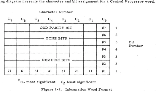
2. 3. 2 CHARACTER.
A character contains seven bits. These bits are numbered 1 through 7, beginning
with the least significant bit position. Bits 1 through 4 are designated the numeric
bits, bits 5 and
6
are the zone bits, and bit 7 is an odd parity check bit. The follow-ing diagram presents the character and bit as signment for a Central Processor word.Character Number
C~
ODD PARITY BIT ~7 7
~6 6
ZONE BITS
f)5 5 Bit
Number
~4 4
~3 3 NUMERIC BITS
~2 2
71
61
51 41 31 21 11 ~1 1>'c
I C7 most significant C~ least significant
Figure 2-2. Information Word Format
A short two-digit notation will sometimes be used in this manual to designate a bit
position in the Central Proces sor word. The first digit will provide the character
number, and the second digit will specify the bit number within that character. Bit
75, for example, designates bit number 5 for the most significant character position.
2.3.3 BIT.
A bit may have a binary value of 1 or ~, in accordance with the position of a toggle, or the direction of magnetization of a single core in Core Memory or of an area on
either magnetic disc or magnetic tape. These bits may be transferred from Core
Memory to the Program Control, Disc Memory Control, or Arithmetic Sections,
where the binary value is recognized and used to access instructions, transfer data,
and perform computation. The 1 status of a toggle is also sometimes considered
[image:35.620.46.572.158.472.2]Section II Paragraph 2. 3. 4
The four numeric bits plus the two zone bits are sufficient to permit 64 alphanumeric character code combinations. Refer to Appendix A for a list of Central Processor, Typewriter/Printer and Punched Card character codes. A seventh bit has been added to each 6-bit character code to provide an odd number of 1 bits. This odd parity status is checked on every data transfer to or from Core Memory, Arithmetic Section registers, Disc Memory, Uni-Record Trunkline devices, and other input-output units. In the event of a parity error, an interrupt request is generated and the Central Processor will enter an interrupt program {unless errors are being ignored under program control}.
2.3.4 ALPHANUMERIC DATA WORD.
An alphanumeric data word may contain several fields of data, each containing fixed-point numeric, alphabetic, or alphanumeric (any combination of symbols, alphabetic, and fixed-point numeric) information. A field consists of any consecu-tive number of characters within the word, and may be specified by many Central Processor instructions. Floating-point instructions, however, process only full-word operands.
The following example presents a Gross Pay field, containing $110.25, and a Rate of Pay field, specifying $2. 25 per hour, within an alphanumeric data word.
EXAMPLE:
I
I
I
I
1 1 5 2 2 5
Gross Pay field Rate/ Pay Field
The programmer must locate the decimal point of numeric fields for fixed-point op-erations. The sign of each fixed-point field within the word is carried in the sixth bit of the least significant character position. A positive sign is indicated by a CJ in bit position six, while a negative sign is provided by a 1. The fifth bit of the least
Section II
Paragraph 2. 3. 5
2. 3.5 FLOATING-POINT DATA WORD.
Floating-point execution may be specified as an option by all full-word arithmetic
instructions and by a numeric compare instruction, paragraph 2.4.5. This option is
provided to extend the range of the operands that participate in these operations.
Floating-point numbers carry and automatically process the decimal point position.
A floating-point data word presents the number as a signed decimal fraction times a
signed integral power of ten. The sign of the fraction and the exponent with its sign
are carried in the zone bits of characters C 4 through C~ in the following format. A 1 bit in a sign position indicates a minus.
Fraction 8 2 8 2
Sign Bit 6
Bit 5 Exponent 4 1 4 1
Sign
"
y I"
y 1\ yNot Used Exponent Exponent
Tens Unit
Digit Digit
The exponent is carried as two binary- coded decimal digits in the zone bits of the
four least significant characters of the data word.
Floating-point numbers can range from .
~~~00~~0
x 10-99
(equals zero) to.99999999
x 1099 .
There is no minus zero in either the mantissa or exponent.I
The following example presents the bit configuration for the floating-point operand,
+ .
0162 x 10- 14, which could be represented in the computer word and in the ex-ample as the normalized quantity,+.
16200000 x 10-15. A floating-point numberis said to be normalized when it is positioned so that the machine decimal point is
EXAMPLE:
Floating-Point Data Word (as it would
appear in a register)
0
0
(/J (/J0
0
1Quantity:
+ .
1 Printouton Line Printer or Typewriter: 1
1
0
f/J f/J
(/J (/J
(/J (/J
1 f/J
1 1
(/)
0
6 2
6 2
2.4 INSTRUCTION WORD FORMAT.
0
10
f/J( +) f/J f/J 1(-) (/J 1
(/J (/J (/J
f/J f/J f/J
f/J f/J f/J
0
0
0
+
+
0
f/J 1 (/J f/J f/J C/J+
0
f/J 1 () f/J C/J f/J+
Section II Paragraph 2. 4x 10- 15
Each Central Processor or input-output instruction is contained in one 8-character word, figure 2-3. Disc Memory instructions, which require three consecutive words, are discussed separately in Sections IX and X. The most significant char-acter (C) of the instruction word specifies the command, the next two charchar-acters (Z and Y) are used normally for field select and address select, but may also specify command modificationG The next most significant character (X) selects one of 1 7 Index register s. The least significant four character s (MMMM) normally provide the unmodified operand or next instruction address. Zone bits 5 and/ or 6
of the X, Z Y, and three least- significant MMMM characters may be used to modify operand access or instruction execution.
Section II
Paragraphs 2. 4. 1 to 2. 4. 2
Character No. C7 Instruction
Characters Zone Bit 6
Zone Bit 5
C
C6
Z Tagged Halt Absolute
C5
C4
C3 C2Y X M M
Floating Flag MASM
Point Return Hold
Normalized MASM
Bring Figure 2-3. Instruction Word Format
2. 4. 1 COMMAND CHARACTER (C).
Cl
c0
M M
MASM Indirect O. A. -1 Address MASM
O. A. +1
The command character (C) specifies one of 34 basic Central Proces sor commands,
6 input-output commands, or designates Disc Memory operation. The Z Y charac-ters and bit options of the instruction word, however, expand the program range to hundreds of individual and distinct Central Proces sor and input~output operations. The different Disc Memory operations are specified by a three-word Disc Memory instruction.
The command character normally provides easy to remember codes in machine lan-guage. (A for Add, M for Multiply, I for Input, etc.) Programs for this Data Proc-essing System, however, will seldom be written directly in machine language. The programmer will normally use LAP, the Librascope Assembly Program, to provide the actual Central Processor instructions. The LAP system permits the use of mnemonic term s for the command code and the different bit options. It allows Index registers and Z Y select characters to be defined symbolically, facilitates access to closed subroutines, provides the programmer with a variety of system macros, permits him to create additional macros, etc. Refer to Appendix D for LAP mnemonics.
2. 4. 2 SELECT CHARACTERS (Z Y).
[image:39.620.47.568.58.268.2]EXAMPLE:
~ Field
Alphanu:meric Data Word C
7 C6 C5
Z = 5, Y=3
..
C
4 C3 C2
Section II Paragraph 2. 4. 3
C
1 Ccj
b. Address Select. Input-Output, Test, Set, Save, Load, and Copy instructions
specify a Trunkline or other input-output device, or designate a signal line, toggle,
or Central Processor register. The least significant five bits of both the Z and Y
characters nor:mally are used for addressing, and are capable of selecting up to
1024 positions or devices. The ZY addresses assigned to Central Processor in-structions are listed in Appendices Band C.
c. Instruction Modify. The Z Y characters also control execution of operations such as the Shift and the Modify Index register instructions. These instructions are
discus sed individually in Section IV.
2. 4. 3 INDEX CHARACTER (X).
Most of the Central Processor, input-~utput, and Disc Me:mory instructions :may
specify index :modification of the operand address. Bits 1 through 5 of the X
char-acter in the instruction word will select one of 17 Index registers. An X value of 0
:means no index operation. Binary values 1 through 15 specify operand address
:modification by one of 15 Index registers, XRl through XRl5, stored in Core
Me:m-ory. These occupy the four least significant character positions of :me:mory
ad-dresses t>00l through 0015, respectively. Binary values of either 16 or 17 designate
address :modification by one of two static Index registers, XR16 or XRI7. Core
:me:mory positions 0016 and 0(> 1 7 are nor:mal storage locations. Binary value s other
than 1 through 1 7 in bits X 1 through X 5 specify no index :modification.
The indexing function will auto:matically add the content of the designated Index
reg-ister to the MMMM operand address of the instruction word. This action precedes
instruction execution and provides an effective operand or next instruction address
equal to MMMM
+
(X), defined as the value of MMMM plus the content of the Xdesignated Index register. Address :modification by XRl through XR15 increases
instruction operation ti:me by one 5-mic rosecond Core Memory cycle. Static Index
Section II
Paragraphs 2. 4. 4 to 2. 4. 5. 1
A MOdify Index Register instruction (0) is available to increment or decrement the content of the Z designated Index register by the Y specified decimal value of from
1 through
9.
If the content of the selected Index register then attempts to become negative or exceed core memory capacity, normal sequential instruction accesscontinues; otherwise the next instruction will be accessed at the effective operand
addres s in the 0 instruction. The indexing option, in conjunction with the D in-struction, facilitates the repetitive use of program instructions and routines.
2. 4. 4 MEMORY ADDRESS CHARACTERS (MMMM).
The MMMM characters of the instruction word in most instructions specify the
un-modified or original Core Memory location of the operand or the next instruction
address. When the address portion of the instruction word is not required, it may be used for other data storage.
The numeric bits of the three least significant characters and bits 1 and 2 of the
most significant character in MMMM specify locations fJ(JfJ(J through
3999
for each Core Memory module. Bits 3 through 6 of the most significant MMMM character provide a binary value of (J through 15, to select one of 16 Core Memory modules. It should be noted that the Central Processor arithmetic instructions providedeci-mal operations. A Convert instruction (P) is available to translate between the four
characterMMMM binary-decimal addres s and an equivalent five character decimal
addresso This instruction is intended to be used in conjunction with arithmetic
operations which modify or provide memory addresses in excess of
9999.
The indexing function, the Modify Index Register instruction, and any
zone-bit-specified MMMM increment-decrement action automatically will provide proper
binary-decimal address modification. These operations process only the numeric
bits of the three least significant MMMM address characters, and all six data bits
of the most significant character. All other bit positions in the Central Processor
word are ignored.
2. 4. 5 ZONE BIT OPTIONS.
2. 4. 5. 1 INDIRECT ADDRESSING. Further operand or next instruction address
modification is provided if bit
6
of the least significant character in the instruction word is a 1. Then the MMMMaddress is incremented by the content of thespeci-fied Index register to provide an indirect effective address. The word at this
indi-rect location again will contain MMMM and X characters, and another indiindi-rect
Section II Paragraphs 2. 4. 5. 2 to 2. 4. 50 3
or next instruction address if the indirect addres s bit is a f/J, or specify the next
in-direct effective memory address if the bit is again a 1.
Assume that an Add instruction word provides an operand address MMMM of
f/J090,
specifies an X Index register 13 whose content is 0010, and the indirect-bitdesig-nator is 1. Since the indirect effective address is f/Jlf/Jf/J, the Central Processor will access this location. Assume that the word at
f/J10f/J
contains an MMMM of 2050, designates an X Index register 9 whose content isf/J125,
and the indirect bit desig-nator is0.
The effective operand addres s is then 2175, and this location will sup-ply the required operand for the Add operation. It should be noted that during theindirect addressing operation all but the MMMM, X, and indirect-bit positions at
any indirect address location will be ignored. All other bit options, as well as the
Z Y characters, are provided by the original instruction word.
2. 4. 5. 2 FLOATING-POINT. Floating-point operation may be specified by all full
word arithmetic instructions (A, S,
+, -,
M, and D) and by the Numeric Compareinstruction (0) if bit Y6 in the instruction word is a 1. Fixed-point execution is selected if the bit is a
0.
This Y6 bit option will be ignored for all other instruc-tions. Floating-point instructions may be indexed, and may specify indirectaddressing.
The operands and/ or result of a floating-point operation will automatically be
nor-malized if bit Y 5 in the instruction word is a 1. This bit option will be ignored for all other instructions and for fixed-point operation.
The actual normalize process varies for the several floating-point instructions.
These instructions are described individually in Section IV.
A normalized floating-point operand has its fraction shifted left, with proper
modi-fication of the exponent, until the most significant digit position in the Central
Processor word is non-zero. Floating Point Instructions are described in
para-graph 4.
6.
2. 4. 5. 3 ABSOLUTE. Absolute execution is specified for the A, S,
+, -,
M, G,D, / and
0
instructions, during either fixed-point or floating-point operation, if bit Z 5 in the instruction word is a 1. This bit option will be ignored for all other instructions. Absolute operation considers the specified field, word, or fractionin Core Memory to contain a positive sign. Standard instruction execution is then
completed, using the algebraic operand held by the relevant Central Processor
Section II
Paragraphs 2. 4. 5. 4 to 2. ~. 5."5
2.4.5.4 TAGGED HALT. Tag control is.
avai1~ble
,
with all instructions. A Tagbutton on the Control Console can be depressed to set a corresponding Central
.
.
,
Processor toggle, which may be program tested, (ZY=5 ]). The ON position ofthe Tag button and bitZ
6
in the i"nstruction word equal to 1 will cause .the Central Processor to Halt after access of the iI\struction word.The Central Processor ignores the tag. bit if the Tag button is OFF. Pressing the
Start button or the Step button on the Control Console, following the Halt, permits
the program to continue with normal instruction execution. The tag control assists
in program debugging by providing an optional Halt preceding execution of any
tagged instructions.
2.4. 5. 5 FLAG RETURN. The address of the instruction word is placed
automat-. .
ically in memory when bit
6
of the X character is a1.
If an interrupt does occur, the stored instruction address represents a return point for the program ..An
x6
flagged instruction has its address stored in the most significant half of one of four Core Memory locations, depending on the type of instruction. The leastsignificant half of these locations is not modified.
a. Memory Address .0~.0l - Central Processor instruction
bo Memory Address 11:/).02 - Disc Memory instruction
c. Memory Address
:/):/):/)3 -
Uni-Record Interface instructiond. Memory Address j}j}j}4 - Input-Output Interface instruction