Published Online May 2016 in SciRes. http://www.scirp.org/journal/cs http://dx.doi.org/10.4236/cs.2016.76072
Performance Analysis of PI and Fuzzy
Control for Modified LCC Resonant
Converter Incorporating Boost Converter
N. Madhanakkumar1, T. S. Sivakumaran21Department of Electrical and Electronics Engineering, Anna University, Chennai, India
2Department of Electrical and Electronics Engineering, Arunai College of Engineering, Tiruvannamalai, India
Received 17 March 2016; accepted 14 May 2016; published 17 May 2016
Copyright © 2016 by authors and Scientific Research Publishing Inc.
This work is licensed under the Creative Commons Attribution International License (CC BY).
http://creativecommons.org/licenses/by/4.0/
Abstract
In this paper, the modified LCC type of series-parallel Resonant Converter (RC) was designed and state-space modeling analysis was implemented. In this proposed converter, one leg of full bridge diode rectifier is replaced with Synchronous Rectifier (SR) switches. The proposed LCC converter is controlled using frequency modulation in the nominal state. During hold-up time, the SR switches control is changed from in-phase to phase-shifted gate signal to obtain high DC voltage conversion ratio. Furthermore, the closed loop PI and fuzzy provide control on the output side without de-creasing the switching frequency. The parameter such as conduction loss on primary and second-ary side, switching loss, core and copper also reduced. Simultaneously, the efficiency is increased about 94.79 is realized by this scheme. The proposed converter with an input of 40 V is built to produce an output of 235 V with the help of ZVS boost converter [1] even under line and load dis-turbances. As a comparison, the closed loop fuzzy controller performance is feasible and less sen-sitive than PI controller.
Keywords
LCC Resonant Converter, Synchronous Rectifier (SR), Fuzzy Controller, PI Controller, State-Space Modeling
1. Introduction
has been developed. The objective of the proposed converter is to provide remarkable efficiency with regulated responses even under fluctuations in line and load sides by modified LCC Resonant Converter and different control techniques. There are various types of resonant converters [2] [3]. Among these, series-parallel resonant converter (SPRC) is preferred in this work. Both series and parallel resonant converter combines to eliminate the lack of no-load regulation for Series Resonant Converter (SRC), circulating current independent of load for Pa-rallel Resonant Converter (PRC). Many converter topologies and techniques have been proposed. One of the most attractive topology is LCC series-parallel resonant converter is provided. Therefore, the LCC resonant converter is widely used in many applications such as electronic ballast for fluorescent lamps, filament heating, SMPS, particularly in high output voltage and low output current applications [4]-[6]. The general power supply block diagram is shown inFigure 1.
Generally, there are two stages in power supply that has a power factor correction (PFC) stage, a front-end DC-DC converter stage [7] [8]. The purpose of PFC stage is to achieve unity power factor and galvanic isolation, shapes the input current to meet the THD requirement. It provides link input voltage Vlink-nom to the DC-DC
conversion stage [9] [10]. This front-end converter stage used to regulate the output voltage precisely. Further-more, to improve the system efficiency after an ac voltage loss certain period of time will maintain the output voltage, called hold-up time. Though there are various techniques for modeling of converter [11] [12], the state-space mathematical modeling is more beneficial than others. The modeling technique is used to analyze the steady state and transient behavior of the resonant tank circuit. The several sections of proposed converter have been discussed here. First the design of proposed converter is to be implemented followed by State Space Ma-thematical Modeling Analysis and Design of Resonant Tank is to be concentrated. Next section inspected on several Performance Analysis of LCC Resonant Converter followed by Design procedure of PI and Fuzzy Con-trollers. Finally sections concluded with simulation results and conclusion of proposed work.
2. Resonant Converter
2.1. LCC Resonant Converter
The LCC resonant converter is now becoming more popular for its easy design and high efficiency, because of zero voltage switching (ZVS) and zero current switching (ZCS) switching conditions. There are many possible combinations of the resonant tank circuit depends upon the inductor and capacitor connections [13]. In this work, LCC resonant tank consist of an inductor (Lr) with series capacitor (Cs) are connected in parallel to the parallel capacitor (Cp). This tank circuit acts as an energy buffer which regulates the energy flow from the input source to output load [14].
In this paper, an SR method is proposed for a new modified LCC resonant converter. It consists of two power MOSFET semiconductor switches for single phase half bridge inverter on the inverter side which gets input from the ZVS boost converter [15] [16]. The transformer secondary side consists of two SR switches 1ø diode bridge rectifier construction. The LCC Resonant Converter Incorporating Boost Converter circuit diagram is shown in Figure 2.
2.2. Zero Voltage Switching Boost Converter
[image:2.595.176.499.618.708.2]The ZVS boost converter is similar to DC-DC boost converter which works under ZVS switching condition thus reduces the switching losses. The capacitive turn-on loss is eliminated by zero voltage switching (ZVS) tech-nique. So, ZVS is more beneficial than ZCS. In this proposed system, the ZVS boost converter is boost up the input voltage of 40 V to 150 V which acts as the input to inverter circuit on the primary side of transformer.
Figure 1. Block diagram of general power supply stages.
AC
Boost PFC Part
Vlink
Clink
DC-DC Conversion
Part
Figure 2. Circuit diagram of LCC resonant converter incorporating boost converter.
The output parameters can be controlled by changing the duty cycle. The ratio of output voltage to input voltage is given in Equation (1).
1 1
O in
in O
V I
V = −D= I (1)
3. State Space Mathematical Modeling Analysis
In this paper, the state-space mathematical modeling technique is adopted for LCC resonant converter based on different operating modes [17] [18]. Here, the state equation is applied only for three operating modes.
3.1. State-Space Analysis
Some of the following assumptions are made while doing the state-space modeling [19] [20]. The assumptions are:
a) The elements such as switches, inductors, capacitors and diodes used are ideal.
b) The effect of snubber and losses includes tank circuit, semiconductor switches and filter losses are neg-lected.
c) The filter capacitor Cf should be large enough than the parallel capacitor CP to produce constant output voltage Vo.
d) The high frequency transformer is ideal with turns ratio n = 1.
e) The input voltage Vdc and output voltage Vo kept constant without ripples in steady state.
3.1.1. Mode A
In mode A, the M1 and SR2 switches are turned on. The tank circuit voltage and resonant current are in-phase.
The resonant capacitor Cs boosts inductor current iL. So both iL(t) and VCS(t) are positive. The voltage of CP is equal to the output voltage Vo, because CP is connected in parallel to filter capacitor Cf. The state-space input and output matrix is given below as Equations (2) and (3).
( )
( )
( )
( )
[
0]
1 d 0 1 d 1 d 0 0 d L s L s dc cs cs s i t
L i t
t L V V
V t V t C t − = + − (2)
And the output equation is,
Vdc La S1 Ca Lb D3 S2 D4 C5 C D6 D5 M1 M2 C2 C1
Lr Cr
D1
D2
C6 RL
[ ]
1 0 0 1 L cs i y V = (3)
With initial condition iL(0) and Vcs(0).
3.1.2. Mode B
In this mode of operation, M2 and SR1 pairs are turned on. The power delivered to both tank circuit and load.
The Cp is connected anti parallel to the filter capacitor. The resonant capacitor VCs(t) and iL(t) are negative. The state-space input and output matrix is given below as Equations (4) and (5).
( )
( )
( )
( )
[
0]
1 d 0 1 d 1 d 0 0 d L s L s dc cs cs s i t
L i t
t L V V V t V t C t − = + + (4)
And the output equation is,
[ ]
1 00 1 L cs i y V =
(5)
With initial condition iL(0) and Vcs(0).
3.1.3. Mode C
All switches are turned off instead of diode pairs. In this mode, the inductor current and tank circuit voltages are out of phase. So the iL(t) decreases faster. So the energy stored in LCC tank is returned to the source. Here, the resonant current may be positive or negative. The state-space input and output matrix is given below as Equa-tions (6) and (7).
( )
( )
( )
( )
( )
( )
[ ]
1 1 d 0 1 d d 10 0 0
d 0 d 1 0 0 d L s s s L cs cs dc s cp cp p i t L L t L i t v t
V t V
t C V t v t t C − − = + (6)
And the output equation is,
[ ]
y =0 (7)3.2. Stability Analysis
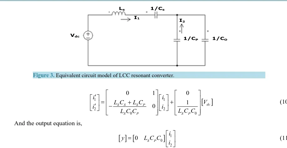
The Stability analysis refers to the stable working condition of a control system [21] [22]. For a stable system, the output response is predictable, finite and stable for a given input. Thus, system stability is determined from the state-space matrix. The Bode plot for the LCC type of Resonant Converter is shown inFigure 4. The equiv-alent circuit model of LCC resonant converter is shown inFigure 3.
The transfer function of LCC Resonant Converter is written in Equation (8),
( )
( )
0
2
s
s p s p
nV S C
mV S =S C C L+C +C (8)
Substituting the values of Ls, Cs and CP, the equation obtained is,
( )
( )
(
)
9 0
2 18 6
470 10
0.8978 10 1.43 10 nV S
mV S S
−
− −
× =
× + × (9)
Figure 3. Equivalent circuit model of LCC resonant converter.
[ ]
1 2 0 0 1 20 1 0
1
0 dc
S S S P
S P
S P
i i
V
L C L C
i i
L C C L C C
′ = + + ′ − (10)
And the output equation is,
[ ]
[
]
10 2
0 S P i
y L C C
i
=
(11)
The Nyquist Plot for the closed loop control of LCC Resonant Converter is shown inFigure 4. The Plot axes are indicated with the poles and zeros of the LCC Resonant converters. From the plot, the roots are lies on the left half of the s-plane and also the root locus doesn’t encircle −1 + j0. So we say that the LCC closed loop con-trol system is stable.
4. Design of Resonant Tank
The values are considered for design the LCC resonant tank is m = Cs/CPratio = 1, Q = 5, y = 1. The Load Resis-tance R=V I0 0=235 2.35=100Ω.
0L 1 L
Q R
Q C
ω
= = (12)
5 100 500
L
Q R
C = × = × =
Resonant frequency f0 is written as f0 = f/y = 127.27 KHz. But,
0 1 2π f LC = 3 1
2π 127.27 10
LC = × ×
The Value of resonant component L and C are Ls = 1.99 μH and C = 959.6 Nf.
5. Performance Analysis of LCC Converter
5.1. Loss Analysis
The transformer of high frequency causes loss on both primary and secondary side. The secondary side is calcu-lated by summing the loss of diode rectifier and SR switches. The transformer size will be reduced because of its high frequency. There is various loss parameters such as conduction loss, core loss, copper loss, switching loss can be calculated as following equations.
2
cond on ds
P =I R (13)
where, Ion is the drain current of the power MOSFET switch, Rds is the drain to source resistance of the switch.
1/Cs
Ls
I2
1/CP 1/CO
I1
Figure 4.Stability analysis of closed loop LCC resonant converter using Nyquist Plot.
But, the loss occur at SR switch is very less than diode rectifier. The Switching loss is calculated as follows,
(
)
2sw o P sw
P = C +C V f (14)
where, Co is the output capacitance of the MOSFET, CP is the Parasitic winding capacitance of the MOSFET switch. fsw is the switching frequency of the Resonant Converter. The total losses are calculated by the sum of conduction loss and switching loss. Figure 5 shows Circuit Simulator employing for loss calculation, where us is blocking voltage. When switch becomes turned ON, the value of us is zero. Is is switching current and TJ is junc-tion temperature of the switch [23]. From Loss Calculation Box which was implemented in MATLAB shown that Pcond = 20.2W and Psw = 10.3W. The loss chart for the LCC Resonant converter is shown inFigure 6.
30.3 W total cond sw
P =P +P = (15)
5.2. Voltage Conversion Ratio
The proposed LCC Resonant converter has different voltage conversion ratios depend on its operation. In the nominal state, the LCC converter operates near Resonant Frequency fr to attain optimum efficiency. The Voltage Conversion Ratio and operating frequency also of the LCC Resonant Converter is analyzed and the correspond-ing graph can be obtained by uscorrespond-ing the equation given below.
(
)
22 2
2
1
π 1
1 1
8 out
in
r V
V
K ω Q ω
ω =
+ − + −
(16)
where V0 is the output Voltage, Vin is the input Voltage, Gain K = CP/CS ratio which is equal to 1. The Resonant frequency and Quality factor of LCC Resonant Converter are given as,
0
1 and
2π L
s p
s p s p
s p Z
Q f
L C C
L
C C C C
C C
+
= =
+
(17)
Figure 5. Circuit simulator employing loss calculation.
Figure 6.Loss chart for the LCC Resonant converter.
5.3. Efficiency
Efficiency calculation is done for different loading conditions.Figure 7shows the efficiency in percentage for variation in loads. The chart could evident that even at full loading condition, the proposed converter able to sustain at 94.79 % of efficiency.
( )
Output Power(
)
(
)
( )
Output Powe Effic
r Total Lo
ienc
s y
sse
OUT
OUT T
P
P P
η =
+ (18)
(
)
Efficiency=V Io o Vo⋅ +Io Ptotal
552.25
100 94.79% 552.25 30.3
η= × =
+
6. Design of PI Controller
The closed loop PI controller is provided on the output side to provide controlled gate signal to switches under different load conditions. Both proportional and integral term is to increase the speed of the response and also to eliminate steady state error. The controller gains KP and KI are tuned by trial and error according to the system
error signal. Figure 8 shows the block diagram representation of PI control based LCC resonant converter.
7. Design of Closed Loop Fuzzy Control
The fuzzy controller is a problem solving control system that operates in a closed-loop system in real time. The limitations of conventional (PI) controller are overcome by fuzzy controller. The fuzzy controller is beneficial because it is very robust, cheap, and simple to design and has the multiple inputs and multiple outputs.Figure 9
shows the block diagram representation of fuzzy control based LCC resonant converter.
Fuzzy logic system is an artificial decision maker based that operates on combinations of Linguistic variable and Boolean logic. Usually fuzzy logic control structure is created from four major elements presented on Fig-ure 10.
Pcond
Psw
PTotal
Switching Signal
IS
TJ
us
0.20
0.65 0.20
0.24 0.11
0.23
0.00 0.10 0.20 0.30 0.40 0.50 0.60 0.70 Primary Conduction Loss (KW)
Secondary Conduction Loss (W) Transformer Copper Loss (W) Transformer Core Loss (W) Switching loss (W) Total Loss (KW)
Figure 7. Plot for efficiency versus different values of loading in %.
[image:8.595.134.500.250.381.2]Figure 8.Block diagram of PI control based LCC resonant converter.
Figure 9.Block diagram of fuzzy control based LCC Resonant converter.
Figure 10. Structure of fuzzy controller.
7.1. Fuzzification
This first phase of fuzzy logic is to deliver the crisp input variables for given fuzzy with the help of membership functions. The inference mechanism formulating the mapping for given input to output. It is done by using mamdani or sugeno type toolbox.
0% 20% 40% 60% 80% 100%
0 20 40 60 80 100
Effic
ie
nc
y %
Loading %
ZVS Boost Converter
(40/150V) Half Bridge Inverter LCC Resonant Tank
SR Switches
in Diode Bridge Rectifier
Load Transformer
PI Controller DC
Input
ZVS Boost Converter
(40/150V) Half Bridge Inverter LCC Resonant Tank
SR Switches in Diode Bridge Rectifier
Load Transformer
FUZZY Controller DC
Input
Rule Matrix
Fuzzy Interference Engine
Fuzzification Defuzzification
[image:8.595.135.497.407.534.2]7.2. Rules and Database
It consist of a database and linguistic control rules are framed by if-then conditional statement with AND/OR logic operation. The fuzzy rules based on the error E, the rate of change of error ∆E and the change in the con-trol signal is the output obtained. Here, 49 rules are used to form rule base table.
7.3. Variable Frequency in Phase Disposition Pulse Width Modulation System
Defuzzification phase converts the fuzzy output from the crisp output. The crisp output is the pulse signal gen-erated to the power switches on the SR switches and half bridge inverter. There are many methods of defuzzifi-cation that have been proposed. The center of gravity is physically appealing among those methods. It is found by calculating the area bounded by the membership function curve. The general structure of fuzzy controller in block diagram representation is shown inFigure 10.
In this proposed work, the seven triangular membership functions are used. The fuzzy rule base table is shown in Table 1based on trial and error method.
8. Simulation Results
[image:9.595.119.517.345.494.2]The simulation results shows the responses of closed loop PI and Fuzzy controller of LCC Resonant Converter with set point of 40 V for nominal load of 100 Ω. TheFigure 11andFigure 12 shows respective PI controller responses of output voltage and current under sudden line disturbances (40 V - 50 V - 40 V) at 0.5sec with no-minal load of 100 Ω and Figure 13 andFigure 14 shows respective PI controller responses of output voltage
Figure 11. Simulated output voltage of LCC RC with sudden line disturbances (40 V - 50 V - 40 V) at t = 0.5 sec (PI Con-troller).
[image:9.595.117.513.537.693.2]Figure 13.Simulated output voltage of LCC RC with sudden load disturbances (100 Ω - 90 Ω - 100 Ω) at t = 0.8 sec (PI Controller).
Figure 14.Simulated output current of LCC RC with sudden load disturbances (100 Ω - 90 Ω - 100 Ω) at t = 0.8 sec (PI Controller).
Table 1. Fuzzy rule base.
E
CE
NB NM NS Z PB PM PS
NB NB NB NM NM NS NS Z
NM NB NM NM NS NS Z PB
NS NM NM NS NS Z PB PB
Z NM NS NS Z PB PB PM
PB NS NS Z PB PB PM PM
PM NS Z PB PB PM PM PS
PS Z PB PB PM PM PS PS
[image:10.595.89.536.488.623.2]Figure 15.Simulated output voltage of LCC RC with sudden line disturbances (40 V - 50 V - 40 V) at t = 0.5 sec (Fuzzy Controller).
Figure 16. Simulated output current of LCC RC with sudden line disturbances (40 V - 50 V - 40 V) at t = 0.5 sec (Fuzzy Controller).
Figure 17.Simulated output voltage of LCC RC with sudden load disturbances (100 Ω - 90 Ω - 100 Ω) at t = 0.8 sec (Fuzzy Controller).
Table 2. Performance evaluation of closed loop fuzzy control with PI control Of LCC resonant converter.
LCC Resonant Converter
Supply Voltage Increase by 10 V (Line disturbance) & Load Resistance decrease by 10 Ω (Load disturbance)
Delay time (msec) Rise Time (msec) Settling time (msec)
FUZZY 20.1 70.1 60.2
[image:11.595.122.517.451.600.2] [image:11.595.87.541.655.719.2]Figure 18.Simulated output current of LCC RC with sudden load disturbances (100Ω - 90 Ω - 100 Ω) at t = 0.8 sec (Fuzzy Controller).
Figure 19. Graphical comparison of simulated performances of closed loop fuzzy control and PI control for LCC RC from
Table 2.
Table 3. Parameters specification for LCC resonant converter.
PARAMETERS VALUES
Input Voltage, Vdc 40 V
Resonant Inductor, Lr 1.99 μH
Resonant Series Capacitor, CS 470 nF
Resonant Parallel Capacitor, CP 960 nF
Load Resistance, RL 100 Ω
Output Voltage, Vo 235 V
Output Current, Io 2.35 A
the results of PI and Fuzzy controlled converter, we could evident that Fuzzy controlled converter had less dis-traction under sudden load and line disturbances.
20.1
70.1
60.2
90.01
95.01
100.02
Delay Time (msec)
Rise Time (msec)
Settling Time(msec)
[image:12.595.91.538.541.685.2]9. Conclusion
In this paper, the modified LCC type of Series-Parallel Resonant Converter was proposed. During hold-up time, the SR switches operate with phase-shifted gate signal to obtain high voltage conversion ratio without reduction in switching frequency. Thus, the closed loop control of LCC resonant converter performance was obtained us-ing fuzzy and PI controller. The simulation results show that the fuzzy controller yields better dynamic perfor-mance even under sudden load and line disturbances. The stability of the system was also analyzed with the help of Nyquist plot. Furthermore, state-space analysis modeling technique is adapted. Likewise, the reduction of loss will lead to attain 94.79% of efficiency. From the simulation results, it is found that the closed loop fuzzy con-trol system is less susceptible to the disturbances than PI.
References
[1] Madhanakkumar, N., Sivakumaran, T.S., Irusapparajan, G. and Sujitha, D. (2014) Closed Loop Control of LLC Reso-nant Converter Incorporating ZVS Boost Converter. International Journal of Engineering and Technology, 6.
[2] Fang, X., Hu, H.B., Chen, F., Somani, U., Auadisian, E., Shen, J. and Batarseh, I. (2013) Efficiency-Oriented Optimal Design of the LLC Resonant Converter Based on Peak Gain Placement. IEEE Transactions on Power Electronics, 28. [3] Oeder, C. (2010) Analysis and Design of a Low-Profile LLC Converter. IEEE International Symposium on Industrial
Electronics, 3859-3864. http://dx.doi.org/10.1109/isie.2010.5637747
[4] Xie, X., Zhang, J., Zhao, C., Zhao, Z. and Qian, Z. (2007) Analysis and Optimization of LLC Resonant Converter with a Novel Over-Current Protection Circuit. IEEE Transactions on Power Electronics, 22, 435-443.
http://dx.doi.org/10.1109/TPEL.2006.889919
[5] Foster, M.P., Gould, C.R., Gilbert, A.J., Stone, D.A. and Bingham, C.M. (2008) Analysis of CLL Voltage-Output Re-sonant Converters Using Describing Functions. IEEE Transactions on Power Electronics, 23, 1772-1781.
http://dx.doi.org/10.1109/TPEL.2008.924835
[6] Duerbaum, T. (1998) First Harmonic Approximation including Design Constraints. Twentieth International Telecom-munications Energy Conference Proceedings, 321-328.
[7] Choi, W.-Y., Kwon, J.-M. and Kwon, B.-H. (2006) High-Performance Front-End Rectifier System for Telecommuni-cation Power Supplies. IEE Proceedings—Electric Power Applications, 153, 473-482.
http://dx.doi.org/10.1049/ip-epa:20050257
[8] de Groot, H., Janssen, E., Pagano, R. and Schetters, K. (2007) Design of a 1-MHz LLC Resonant Converter Based on a DSP-Driven SOI Half-Bridge Power MOS Module. IEEE Transactions on Power Electronics, 22, 2307-2320.
http://dx.doi.org/10.1109/TPEL.2007.904203
[9] Yang, B., Lee, F.C., Zhang, A.J. and Huang, G. (2002) LLC Resonant Converter for Front End DC-DC Conversion.
Seventeenth Annual IEEE Applied Power Electronics Conference and Exposition, 1108-1112.
[10] Cheng, J.H. and Witulski, A.F. (1998) Analytic Solutions for LLCC Parallel Resonant Converter Simplify Use of Two- and Three-Element Converters. IEEE Transactions on Power Electronics, 13, 235-243.
http://dx.doi.org/10.1109/63.662828
[11] Lee, B., Kim, M., Kim, C., Park, K. and Moon, G. (2009) Analysis of LLC resonant Converter Considering Effects of Parasitic Components. International Telecommunications Energy Conference, 1-6.
http://dx.doi.org/10.1109/intlec.2009.5351740
[12] Ivensky, G., Bronshtein, S. and Abramovitz, A. (2011) Approximate Analysis of Resonant LLC DC-DC Converter.
IEEE Transactions on Power Electronics, 26, 3274-3284. http://dx.doi.org/10.1109/TPEL.2011.2142009
[13] Lin, B.-R. and Du, Y.-K. (2015) Medium Voltage Resonant Converter with Balanced Input Capacitor Voltages and Output Diode Currents. Journal of Power Electronics, 15, 389-398. http://dx.doi.org/10.6113/JPE.2015.15.2.389
[14] Beiranvand, R., Rashidian, B., Zolghadri, M.R. and Alavi, S.M.H. (2010) Designing an Adjustable Wide Range Regu-lated Current Source. IEEE Transactions on Power Electronics, 25, 197-208.
http://dx.doi.org/10.1109/TPEL.2009.2027237
[15] Steigerwald, R.L. (1988) A Comparison of Half-Bridge Resonant Converter Topologies. IEEE Transactions on Power Electronics, 3, 174-182. http://dx.doi.org/10.1109/63.4347
[16] Liu, T., Zhou, Z., Xiong, A., Zeng, J. and Ying, J. (2006) A Novel Precise Design Method for LLC Series Resonant Converter. Twenty-Eighth International Telecommunications Energy Conference, 1-6.
http://dx.doi.org/10.1109/intlec.2006.251606
http://dx.doi.org/10.1109/TPEL.2011.2168545
[18] Lu, B., Liu, W., Liang, Y., Lee, F.C. and van Wyk, J.D. (2006) Optimal Design Methodology for LLC Resonant Con-verter. Twenty-First Annual IEEE Applied Power Electronics Conference and Exposition, 2, 6.
[19] Batarseh, I. (1995) State-Plane Approach for the Analysis of Half-Bridge Parallel Resonant Converters. IEE Proceed-ings—Circuits, Devices and Systems, 142, 200-204. http://dx.doi.org/10.1049/ip-cds:19951890
[20] Bhat, A.K.S. (1998) A Generalized Steady-State Analysis of Resonant Converters Using Two-Port Model and Fouri-er-Series Approach. IEEE Transactions on Power Electronics, 13, 142-151. http://dx.doi.org/10.1109/63.654968 [21] Batarseh, I., Liu, R., Ortiz-Conde, A., Yacoub, A. and Siri, K. (1994) Steady State Analysis and Performance
Charac-teristics of the LLC-Type Parallel Resonant Converter. Power Electronics Specialists Conference, 597-606.
http://dx.doi.org/10.1109/pesc.1994.349675
[22] Lazar, J.F. and Martinelli, R. (2001) Steady-State Analysis of the LLC Series Resonant Converter. Sixteenth Annual IEEE Applied Power Electronics Conference and Exposition, 2, 728-735. http://dx.doi.org/10.1109/apec.2001.912451 [23] Drofenik, U. and Kolar, J.W. A General Scheme for Calculating Switching- and Conduction-Losses of Power Semi-conductors in Numerical Circuit Simulations of Power Electronic Systems. Power Electronic Systems Laboratory (PES), ETH Zurich ETH-Zentrum, Zurich. www.pes.ee.ethz.ch
[24] Kutkut, N.H., Lee, C.Q. and Batarseh, I. (1998) A Generalized Program for Extracting the Control Characteristics of Resonant Converters via the State-Plane Diagram. IEEE Transactions on Power Electronics, 13, 58-66.