International Journal of Emerging Technology and Advanced Engineering
Website: www.ijetae.com (ISSN 2250-2459, ISO 9001:2008 Certified Journal, Volume 9, Issue 10, October 2019)
179
A Review Paper on Gain and Bandwidth Enhancement of
Microstrip Patch Antenna
Pragya Lariya
1, Dr. Mukul Shrivastava
21M.Tech Scholar, 2HOD, EC Department, LNCTE BHOPAL
Abstract-- This paper presents the various techniques
of gain improvement in Micro-strip Patch Antennas (MPAs).Today antenna designers are paying additional focus on micro-strip patch antennas, due to its various benefits in field of communication, like high reliability, light-weight, easy fabrication etc. however despite of its bountiful benefits, patch antennas also experience some drawbacks like low gain and narrow bandwidth. These drawbacks is overcome by taking care of some parameters within the style of antennas MPAs are characterised by their parameters. the various parameters needed are radiation pattern, Voltage standing wave ratio, Reflection Coefficients etc. Among all the parameters Gain and bandwidth plays a very important role within the efficiency of MSAs. There are various designing factors affecting the radiating characteristics of antenna like patch height, feeding techniques, substrate utilized in manufacturing of antenna etc. in this paper, analytic review is completed on rising the gain of an antenna. The paper contains of a quick study in feeding techniques, parasitic patch components, introduction of slots, dual feed, shorting pin, air gap and recently introduced construct of defective ground structure that enhances the gain and bandwidth of antenna while not increasing its height
Keywords-- Micro-strip patch antennas, feeding
techniques, gain, bandwidth.
I. INTRODUCTION
With the dynamic development in wireless communication technology the requirement for compact size, lightweight weight, cost effective and low profile antenna has accumulated considerably. Micro-strip antennas were designed to realize these necessities. Recent development within the field of wireless communication systems to comprehend high speed data transfer between PCs, laptops, cell phones etc, result in antenna with improved gain and bandwidth. WLAN and Wi-MAX evolved as two industrial communication standards to produce high speed. For this also micro-strip antenna is needed.
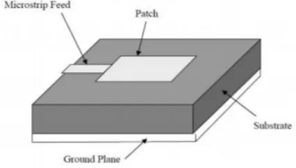
[image:1.612.336.549.408.529.2]One of the foremost want for contemporary communication devices is that the operation on the broader band in order that the antenna will support high speed operations, multimedia communication and lots of alternative broad band services. Easy diagram of micro-strip patch antenna show within the fig.1 in this fig show that micro-strip antenna comprises a patch (like circular, rectangular, ellipse, ring or the other kind of shape)and ground plane between theme a substrate, having specific worth of dielectric constant. Dimension of ground plan and substrate plan are larger than compare to patch. Dimension of the patch dimension of patch depend upon material constant of the substrate and resonance frequency of the antenna. Micro-strip feed line and patch are connected by exposure etched on substrate.
Fig. 1 Simple diagram of micro-strip antenna
Size of antenna decrease by increasing the number of iteration and bandwidth of micro-strip antenna increase by a number of slot over the patch. If bandwidth increase then Q factor decrease and inductance increase by equation (1)
….eq (1)
II. LITERATURE REVIEW
International Journal of Emerging Technology and Advanced Engineering
Website: www.ijetae.com (ISSN 2250-2459, ISO 9001:2008 Certified Journal, Volume 9, Issue 10, October 2019)
180
Flux unit innovation has been utilised within the zones of radio identification and lengthening,detecting and military correspondences from the previous 1 / 4 century but from the previous one decade inquiries regarding have an inclination to indicate interest towards creating the flux unit additional fitting for processed correspondence equally with respect to the prosperity applications. Flux unit has been speedily progressing as a promising high rate remote correspondence innovation. The upsides of broadband region unit High Security since it's low traditional transmission management that creates it proof against recognition and interference. Flux unit beats zone unit time-tweaked with codes clear to every transmitter and recipient. Flux unit beats even have Resistance to Interference. Some additional benefits incorporates sturdy Penetration capability, less battery Power Consumption, High Performance in Multipath Channels. The fundamental reception equipment parameters vital to deliver background info are impedance bandwidth measured by the characterization of both the VSWR and RL. The assorted different parameters are directivity, Bandwidth, Gain, Polarization, Antenna power and radiation patternIII. ANTENNA GEOMETRY AND DESIGN
A low profile antenna is design as it use from 400 MHz to 38GHz much, and it may be expected that the technology can presently be 60 GHz and on the far side that is very simple to design and is value effective. In designing of antenna the propagation constant for a wave in the micro-strip substrate should be properly illustrious so as to predict the various parameters like resonant frequency , resonant resistance etc. Antenna designers have found that the foremost sensitive parameter in micro-strip antenna performance estimation is dielectric constant of a substrate material, and also the manufacturers tolerance on is typically inadequate. The dielectric substrate material used in micro-strip antenna are generally classified in to relative dielectric constant vary of 1 to 2(low dielectric constant), 2to4 (medium material constant), and four to 10(high dielectric constant). sometimes a low dielectric constant material with low loss tangent like air, foam etc is value effective .The thick and low dielectric constant substrate material are needed to enhance the bandwidth of the antenna. The substrate material is covered with required conducting material of antenna pattern which is backed by conducting ground plane.
3.1.Antenna Feeding To Improve the Gain: Micro-strip feed:
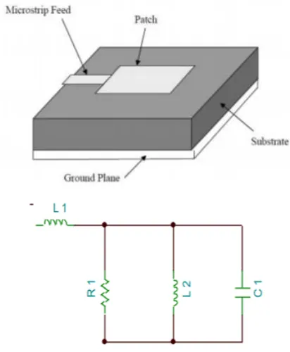
[image:2.612.338.544.245.495.2]In this type of feeding method, a conducting strip is linked directly to the boundary of the Micro-strip patch. The conducting strip is having smaller width as compared to the patch. This feed arrangement has a key advantage, that the feed and patch can be etched on same substrate which makes it a planar structure.
Fig 2. Micro-strip fed patch antenna and its equivalent circuit
International Journal of Emerging Technology and Advanced Engineering
Website: www.ijetae.com (ISSN 2250-2459, ISO 9001:2008 Certified Journal, Volume 9, Issue 10, October 2019)
181
3.2 Coaxial feed:
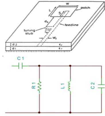
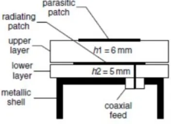
[image:3.612.350.547.143.304.2]The coaxial feed also known as probe feed is broadly used technique for feeding Micro-strip patch antennas. in this technique the internal conductor of the coaxial connector is force out through the dielectric and soldered on the radiating patch, whereas the external conductor is hooked up to ground plane. The key advantage of this coaxial feeding scheme is that it will be placed at any desired position within the patch to facilitate its match with input impedance. However, main hindrance to this feeding technique is that it's difficult to model. Since a hole needs to be trained within the substrate and also the connector stick outside the ground plane, that isn't creating it a whole planar structure for thick substrates. Also, for thicker substrates, the increased probe length makes the input impedance a lot of inductive that leads to impedance matching issues.
Fig.3. Coaxial fed patch antenna and its equivalent circuit
3.3 Aperture Coupled feed:
[image:3.612.62.285.338.517.2]In aperture coupling feed and ground plane with aperture is sandwiched between 2 totally different substrates, to produce electromagnetic coupling from feed to the radiating patch structure. The radiating patch part is inscribed on the highest of the antenna substrate and also the micro-strip feed line is etched on the bottom of the feed substrate so as to get aperture coupling. The thickness and dielectric constants of those 2 substrates would be chosen on an individual basis to optimize the various electrical functions of radiation and electronic equipment. The coupling aperture is placed ideally at the centre location below the patch that results in lesser cross-polarization because of symmetric in configuration.
Fig 4. Aperture coupled fed patch antenna and its equivalent circuit.
3.4 Proximity Coupled feed:
Proximity coupled feed is additionally known as because the electromagnetic coupling scheme. in this technique, two dielectric substrates are used specified the feed line is placed between the 2 substrates and therefore the radiating patch is found on top of the upper substrate. The key advantage of this feeding technique is that it eliminates spurious feed radiation and provides terribly high bandwidth. This theme additionally provides various between 2 totally different dielectric media, one for the patch and another one for the feed line to optimize the individual performances. The key disadvantage of this feeding scheme is that it's complicated to fabricate as a result of each the dielectric layers want correct alignment.
[image:3.612.351.534.500.701.2]International Journal of Emerging Technology and Advanced Engineering
Website: www.ijetae.com (ISSN 2250-2459, ISO 9001:2008 Certified Journal, Volume 9, Issue 10, October 2019)
182
IV. GAIN AND BANDWIDTH ENHANCEMENT TECHNIQUESApart from the various feeding techniques, there are varied different strategies adopted in recent times, to improvise the inherent issue of gain and bandwidth in micro-strip antennas. A brief insight concerning such common strategies is printed as below:
A. Slotted Patch:
[image:4.612.349.535.134.332.2]The conventional micro-strip antenna has slim bandwidth; one in all standard techniques to reinforce the bandwidth is completed by cutting slots within the patch of 0.5 wavelength on the specified resonance frequency. The slots are deep-rooted on the patch to reinforce the impedance matching, particularly at higher frequencies. This distribution on the patch is modified as a results of the cut slots, thus the input impedance and current path length changes. By adding new slots into the patch, new resonance frequencies are created. The positions and dimensions of the slots ought to be properly optimized where the primary 2 broadside radiation modes of the radiating patch are flustered where the resonance frequencies of the patch become near one another to realize a wider information measure. Cutting slots technique on the radiating patch is effectively wont to cut back the size of the micro-strip antenna and make multiple frequency bands at the specified frequency vary by optimizing the slots configurations to supply the desired resonant mode. Slots withdraw the patch are of various shapes. The ordinarily used slots are . U-slot, H-slot, T-slot, E-slot etc. information measure of 30.3% has been achieved by etching an E-shaped slot in a rectangular patch. Impedance bandwidth of twenty six is achieved by cutting a u-shaped slot in. in a very style of C-slotted patch is planned to reinforce the gain and supply a bandwidth of 50 from 1 ghz to 3 GHz. C-SLOT antenna is shown in Fig. 6
[image:4.612.89.247.555.711.2]Fig. 6 C-Shaped Slotted Antenna
Fig. 7 Circular patch antenna with horizontal slots
The bandwidth of micro-strip antenna depends on the standard factor. Hence, once the patch id is modified by slots, it stores less energy at a lower place the patch and also the quality issue degrades. So, it provides higher radiation. A circular patch with reflected horizontal slots is designed by Ah san et al. as shown in Fig.7. This configuration can do lower resonance frequencies because of the extension of this distribution with the elemental resonant mode.
B. Parasitic Patch/Multi-Resonator:
International Journal of Emerging Technology and Advanced Engineering
Website: www.ijetae.com (ISSN 2250-2459, ISO 9001:2008 Certified Journal, Volume 9, Issue 10, October 2019)
[image:5.612.370.509.135.294.2]183
Fig 8. Stacked Patch antenna with Parasitic element
C. Metallic Rings:
For circular patch antenna, metallic rings around the active patch are used to scatter the surface wave to reinforce the radiation. When magnetism waves hit an interface that has small dimensions compared to the wavelength of the incident wave, the electromagnetic waves are scattered altogether directions. The scattered waves are superimposed to the incident waves ensuing in-phase and out-of-in-phase interference and therefore the rest will reradiate by the antenna. Based on this idea, inserting metallic rings around the main patch helps scatter the surface waves and to convert it to house wave to reinforce the gain of the micro-strip patch antenna. Circular patch antenna enclosed by 2 metallic rings is projected in and therefore the pure mathematics is shown in Fig ten. The proposed style provides improvement of 6.7 dB within the gain compared to the standard antenna while not the metallic rings.
[image:5.612.84.260.143.271.2]Fig 9. Electromagnetically coupled multilayer structure (a) normal geometry (b) inverted geometry
Fig. 10 Circular patch antenna with metallic rings.
D. EBG:
[image:5.612.63.273.522.662.2]International Journal of Emerging Technology and Advanced Engineering
Website: www.ijetae.com (ISSN 2250-2459, ISO 9001:2008 Certified Journal, Volume 9, Issue 10, October 2019)
[image:6.612.116.223.139.293.2]184
Fig. 11. Two-dimensional mushrooms like EBG surfaces (a) Top view (b) side view.
E. Defected Ground Structure (DGS):
Defected ground structures concept has been developed recently and that they are achieved by engraving an easy defect of any form on ground plane. due to these structures this is disturbed within the ground plane. This ultimately leads to handling excitation and propagation of radio waves across the substrate layer. DGS configuration additionally helps to vary transmission line parameters viz. inductance and capacitance. The defect in ground may be modified consequently from easy form to complicated shape so as to attain desired performance. In micro-strip antennas, defective ground structures have various benefits within the field of transmission lines, couplers, dividers, power amplifiers, oscillators and combiners.
Fig. 12 .Periodic defected ground plane
V. CONCLUSION
Micro-strip patch antenna is wide used due to its several useful benefits but at the same time it's having many alternative drawbacks like lower gain.
In this paper we've studied the various gain improvement techniques and that we have make a case for the way to decrease the various parameters to increase the gain. Proximity coupled Micro-strip Antenna is that the best way to increase the gain. The 3 parameters will be at the same time balanced by the use of variety of micro-strip antenna topologies and composite improvement techniques. popular feeding ways of micro-strip antenna are summarized in this manuscript. It's determined that contacting methods like micro-strip and coaxial feed are simple and implement. However, non-contacting techniques like aperture coupled feed and proximity coupled feed can do wider bandwidth and better gain however they're troublesome to implement because of the alignment of multi-substrates.
REFERENCES
[1] C. A. Balanis, “Antenna theory analysis and design”, 2nd edition, John Wiley and Sons, 2009.
[2] M. N. Aktar, M. S. Uddin, M. R Amin, and M. M. Ali “Enhanced Gain and Bandwidth of Patch Antenna Using EBG Substrates,” International Journal Of Wireless &Mobile Networks (IJWMN), Vol. 3, No. 1, Feb. 2011.
[3] Gonzola, D. Maagt, and Sorola “Enhanced patch-antenna performance by suppressing surface waves using photonic-band gap substrates,” IEEE Trans. Microwave Theory Tech., Vol. 47, pp. 2131-2138, Nov. 1999.
[4] A. Rivera-Albino and C.A. Balanis, “Gain Enhancement in Microstrip Patch Antennas Using Hybrid Substrates,” IEEE Antennas and Wireless Propagation Letters, vol. 12, pp. 476-479, April 2013.
[5] H. Attia and L. Yousefi, “High-Gain Patch Antennas Loaded with High Characteristic Impedance Super strates,” IEEE Antennas and Wireless Propagation Letters, vol. 10, pp.858-861, August 2011. [6] Z. N. Chen, “Broadband probe-fed plate antenna,” in Proc. 30th Eur.
Microwave Conf., pp. 1–5, Oct. 2000.
[7] S. B. Yea, and Z. N. Chen, “Micro-strip patch antennas with enhanced gain by partial substrate removal,” IEEE Transactions on Antennas and Propagation, vol. 58, no. 9, September 2010. [8] S. Kumar Sharma and M. Rattan, “Analysis of Broad Banding and
Minimization Techniques for Square Patch Antenna” IETE journal of research, vol. 56, no. 2, April 2010. [9] D. Chen, and C. H. Cheng, “A novel compact ultra-wideband (UWB) wide slot antenna with via holes” Progress In Electromagnetics Research, vol. 94, pp. 343- 349, 2009. [10] S. S. Yang, A. A. Kishk, and K. Lee “Frequency Reconfigurable U-slot Micro-strip Antenna” IEEE antenna and wireless propagation letters vol. no. 7, 2008. [11] F. Yang, X. Zhang, X. Ye, Y. R. Samii transactions on antennas and propagation,
[9] Tandel Tejal, et al, L- Slot Rectangular Microstrip Patch Antenna for WLAN Application. IJLTEMAS, Volume IV, Issue XII, December 2015
[image:6.612.90.246.503.654.2]International Journal of Emerging Technology and Advanced Engineering
Website: www.ijetae.com (ISSN 2250-2459, ISO 9001:2008 Certified Journal, Volume 9, Issue 10, October 2019)
185
[11] S Samundra ,et al, design a rectangular microstrip patch antennaarray for c band scatterometer and MBI. publice by IEEE, INDICON 2016.
[12] Xiaosheng Geo, et al.Design dual band Embedded inverted T-slot circular microstrip patch antenna .
[13] M. R. Ahsan, M. T. Islam, M. H. Ullah, M. J. Singh, M. T. Ali, “Metasurface Reflector (MSR) Loading for High Performance Small Microstrip Antenna Design,” PLOS ONE, vol 10, no 5, pp 1-20, May 2015.
[14] S. Wi, Y. Lee, and J. Yook “Wideband Microstrip Patch Antenna With U-Shaped Parasitic Elements” IEEE transactions on antennas and propagation, vol. 55, no. 4, April 2007.
[15] C. K. Wu and K. L. Wong, “Broadband microstrip antenna with directly coupled and gap-coupled parasitic patches”, Microwave Opt. Technol. Lett. 22, 348–349, Sept. 5, 1999.
[16] J. Anguera, G. Font, C. Puente, C. Borja, and J. Soler, “Multifrequency microstrip patch antenna using multiple stacked elements,” IEEE Microwave and Wireless Components Lett., vol. 13, no. 3, pp. 123-124, March 2003.
[17] S. I. Sheikh, W. Abu-Al-Saud, and A. B. Numan “Directive Stacked Patch Antenna for UWB Applications” International Journal of Antennas and Propagation Volume 2013, pp. 1-6, Nov. 2013. http://dx.doi.org/10.1155/2013/389571.
[18] Y. H. Cho., C. Pyo and J. Choi “Gain Enhancement of Microstrip Patch Antenna Using Parasitic Metallic Bar,” IEEE AP-S, vol. I, pp. 728 -731, 2003.
[19] A. Kumar, M. Kumar, “Gain Enhancement in Microstrip Patch Antennas Using Metallic Rings,” American Journal of Engineering Research, vol. 3, no. 7, pp. 117-124, 2014.
[20] F. Yang, Y. R. Sami, “Electromagnetic band Gap Structures in Antenna Engineering,” Cambridge University Press 2009.
[21] R. Gonzalo, P. Maagt, and M. Sorolla, “Enhanced Patch-Antenna Performance by Suppressing Surface Waves Using Photonic-Bandgap Substrates,” IEEE Transactions on Microwave Theory and Techniques, vol. 47, pp. 2131-2138, Nov. 1999