A Combined Approach of IVC and GR for Leakage Power
Reduction in CMOS VLSI Digital Circuit
Uday Panwar
Department of ECE, MANIT Bhopal, India
Kavita Khare
Department of ECE, MANIT Bhopal, India
ABSTRACT
In Deep Sub-Micron (DSM) technology, leakage power dissipation consumes the substantial percentage of the total power dissipation and rises exponentially according to the International Technology Roadmap for Semiconductor (ITRS). Leakage power decreases battery life for the entire portable battery operated device such as mobile phones, laptop and cam coder etc. VLSI design constraints are always area, power and delay. To reduce the leakage power losses several techniques has been proposed that proficiently reduces leakage power dissipation Leakage power in CMOS VLSI circuits can be controlled at the circuit level. This paper has considered two run time leakage reduction mechanics i.e. Input Vector Control (IVC) and Gate Replacement (GR). When the first technique is applied on the CMOS circuit, 30% average leakage power reduction is achieved where as 46% of average leakage power is reduces due to GR technique. The Maximum leakage reduction is achieved of 41.2% and 73% due to IVC and GR techniques respectively. These techniques have been applied on ISCAS benchmark circuit C17 using TSMC0.18um technology file on HSPICE simulator.
Keywords
Leakage current, Deep Sub Micron technology, IVC, Gate Replacement
1.INTRODUCTION
The need for lower power consumption and circuit densities has made it necessary to scale down the supply voltage in CMOS logic circuits. To maintain the circuit speed, threshold voltage should also scale down with the supply voltage. This results in increasing leakage current as the leakage current varies exponentially with the threshold voltage [3]. If this trend continues, leakage power will soon be in the same order as the dynamic power. Estimating leakage power in the early stages of VLSI circuit design is important for optimizing the total power dissipation.
This made the researchers to find ways to control and minimize the leakage currents in the modern CMOS technologies. Two important categories for minimizing the leakage current are device level and circuit level methods. In other words, Design time and Run time techniques. For design time technique, Dual threshold CMOS is used; where, transistors with low threshold voltage (Vth) are used in critical paths and high Vth transistors for non-critical paths [4]. Another approach is to use the Multi threshold CMOS (MTCMOS); in which high threshold voltage transistors are placed in series with low threshold circuit has been used with sleep signals to reduce leakage current in sleep mode [5].For Run-Time technique, methods such as the use of transistor stacks, sleep transistors, forward and reverse body biasing, and dynamic Vth scaling are available [6-7].
All of the mentioned techniques require a lot of processing. There are several leakage mechanisms contributing to the OFF current of a MOS transistor in short channel devices. Out of which Sub-threshold leakage and gate leakage are dominant. The dominating leakage mechanism depends on device size, channel dimensions, operating conditions, technology node, and other transistor parameters. The researchers have depicted that Input-vector control to be a very efficient method for leakage power reduction [8]. The basic concept in this technique is forcing the logic of the combinational circuit into a low-leakage state during the off state of the circuit. This state makes sure that more number of transistors will be in off state so that the leakage is less and it will use those multiple off state transistors in stacks [1][8]. There are many methods for determining the least leakage input vector. In [1], an algorithm named Fast Input Vector (FIV) for calculating minimum input vector has been given. In [10], an algorithm is presented that replaces the gates in a circuit in an effort to reduce the standby leakage of the circuit. But all these methods don’t use the circuit topology and dependency information. And also, some methods require a lot of simulations for calculating leakage of the circuit, which is time consuming, especially for bigger circuits. A heuristic approach for determining the low leakage sleep state vector for a given circuit is mentioned in [9]. But the time complexity of this approach is somewhat high.
2. PREVIOUS WORK
Several techniques were proposed to get minimum leakage input vectors; the most of these are based on heuristics, so their results are not optimal. In [13], an Integer Linear Programming (ILP) is presented to compute an input vector that can be applied to the primary inputs of the circuit in standby mode in order to minimize leakage power. An appropriate linear relaxation to provide a lower bound on the integer optimum and then employ a technique called randomized rounding to round the solution to the linear relaxation, which is typically fractional, to an integer solution. The problem is formulated as ILP in two different ways. One scheme consists of relaxing the ILP formulation to obtain a lower bound on the minimum leakage power that is dissipated by the circuit. The linear relaxation of the first ILP formulation is shown theoretically to be of poor quality, while the relaxation to the second ILP formulation is shown to work much better in practice. ILP is not optimal and needs large runtime.
34 additional circuitry, it modifies the original logic design to
force the combinational logic into a low leakage state during an idle period. To find such a low leakage state, they have developed an efficient algorithm that determines a good input vector using a sampling of random vectors. The size of sampling is determined a priori user-supplied quality measures. They have demonstrated this method on the ISCAS-89 benchmark circuits and shown leakage power reduction of up to 54%. This algorithm is poor and not optimal.
In [15], a genetic algorithm was recommended to overawe the problem of MLV Genetic algorithm has an exponential solution space concerning the number of primary inputs. In this algorithm, the chromosomes are represented by the input vectors, and calculation process of the circuit leakage current represents the fitness function. The algorithm selects the parents randomly to make crossover between them to produce the new children. At the end of the method, the parent with the least leakage current is chosen as the best vector. In general, Genetic Algorithm applications are not optimal and need exponential space complexity and large runtime. In [16] a fast algorithm is proposed having the same concept of controllability, which is widely used for fault tolerance detection. In this algorithm, the controllability of each gate in the circuit is calculated. The algorithm eliminates the least cost nodes. The final situation is achieved by eliminating all the nodes in the list. The simulation results showed that the results vectors are among 5% of the best vector obtained from 100,000 random vectors, but it requires a large run time. In [2], Presents graph based algorithms for estimating the maximum leakage power. These algorithm are pattern-independent and do not require simulation of the circuit. Instead the circuit structure and the logic functionality of the component in the circuit are used to create a constraint graph. The problem of estimating the maximum leakage power is then transformed to an optimization problem on the constraints graph. Efficient algorithms on the graph are used to estimate the maximum leakage power dissipated by a circuit comparison with exhaustive/long simulations for MCNC/ISCAS-85 benchmark circuit is presented to verify the accuracy of the method.
The work done till now is based mostly on heuristic approach [8], [17], [18], [19] and have large time complexity.
3. MOTIVATION
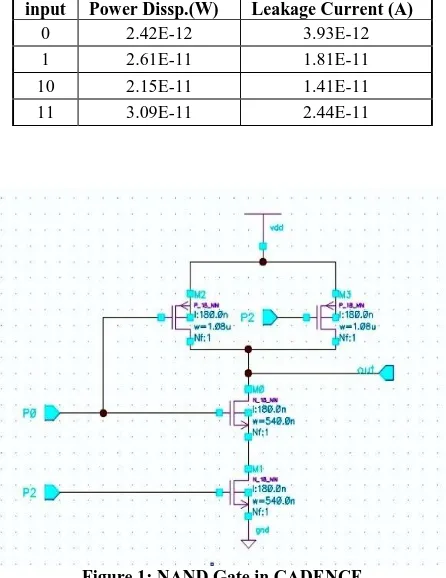
IVC utilizes the stacking effect of the circuit where more off transistor in series reduced the leakage. In logic circuit leakage is directly relating with the input of the gate. It means among all possible combination some input values give least leakage than other. Table1 shows the leakage power dissipation of NAND logic. Data obtained by simulation in Synopsys HSPICE using the 180nm TSMC model at 1.8V supply voltage.
It is seen from Table 1, Shifting a logic gate in its minimum leakage vector (00 as in the case of NAND logic) can decreases leakage by about 92.2% of the Worst Leakage State WLS (i.e. 11 as in the case of NAND logic) [12]. In combinational circuit every logic gates are directly or indirectly depends on the output of the other logic gate input. It is concluded that an exhaustive approach is required to find a minimum leakage vector for a particular circuit as compared to all of its possible input combinations. But if logic depth is too large, only IVC technique is unable to control the leakage of overall circuit. This paper gives a survey on IVC and GR techniques which helpful to overcome such kind of problem
based on logic depth of the given circuit. Here Figure1 shows the NAND gate representation by using CADENCE VIRTUOSO.
TABLE 1: NAND logic with 2 input
input Power Dissp.(W) Leakage Current (A)
0 2.42E-12 3.93E-12
1 2.61E-11 1.81E-11
10 2.15E-11 1.41E-11
11 3.09E-11 2.44E-11
[image:2.595.317.540.137.426.2]
Figure 1: NAND Gate in CADENCE
4. PROPOSED APPROACH
This paper considers two run time leakage reduction mechanisms and applied on a CMOS VLSI circuit. The IVC technique is based on input pattern detection for the minimum leakage pattern during run time of the device. Some pseudo steps are given for detection Minimum Leakage Vector (MLV).Figure 2 represents the ISCAS benchmark circuit C17.
4.1. Pseudo Steps for finding MLV
Assumption:
Read the netlist of the given circuit. Convert it into a graph.
Consider node as a transistor and link as an interconnection. 1) Select primary input from its initial value to final
value or a threshold value.
2) Check for the transistor which is in OFF states in each path of the graph at a given input.
3) If more than one transistor having OFF state in a path there is no leakage takes place.
4) This process counts the number of OFF transistor in a circuit at every input pattern. And a pattern which gives the minimum leakage set as a MLV.
5) Calculate leakage of the circuit.
4.2. Pseudo steps for GR
2) Replace this gate with another variation of it temporary. (i.e. NAND2 => NAND with SLEEP transistor as a variation)
3) Check for the leakage power reduction. If Power is reduce of the circuit this replacement make permanent otherwise no replacement is done. 4) Finally a circuit with least leakage at the given input
pattern is achieved.
5. SIMULATION RESULTS
Previous section gives the procedure about how to calculate leakage power of the given CMOS circuit. All the leakage
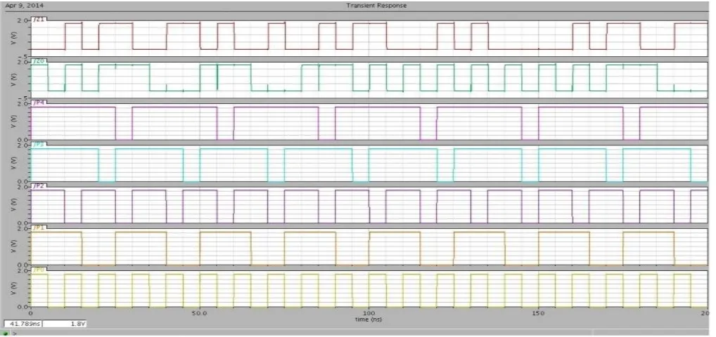
[image:3.595.56.566.196.467.2]reduction techniques and proposed techniques are simulated using HSPICE simulator by Synopsys for two inputs NAND and C17 benchmark circuit. The given approach combines the effect of IVC and GR transistor technique. Figure 3 shows the transistor level representation of C17 circuit using CADENCE VIRTUOSO Schematic Editor. The output waveform of the C17 circuit for different combinations of the input patterns is shown in Figure 4.
Figure 3: ISCAS C17 Circuit
[image:3.595.54.563.504.744.2]36 The given approach has been implemented in C (as it is the
fastest one) and it was checked with an ISCAS benchmark circuit C17. The results are compared against the best vector obtained from the leakage values obtained for all the possible input combinations in HSPICE simulator. The leakage results
[image:4.595.57.564.131.329.2]shows in Figure 4 and Figure 5 gives the comparison between both IVC and GR techniques.
Figure 4 gives the leakage power of the conventional circuit C17 with IVC and GR approach
Figure 5 shows the percentage reduction of leakage power of C17 benchmark circuit
6. CONCLUSION
If a low leakage input vector is applied then the total leakage of the circuit can be minimized in the sleep state. In this paper, an approach is given which determines the MLV of the given circuit. It uses the concept of patterns mining of the circuit and also uses the functional dependencies among the gates in the circuit to search the required input vector. Input Vector Control (IVC) and Gate Replacement (GR). When the first technique is applied on the CMOS circuit, 30% average leakage power reduction is achieved where as 46% of average leakage power is reduces due to GR technique. The Maximum leakage reduction is achieved of 41.2% and 73% due to IVC and GR techniques respectively. These techniques have been applied on ISCAS benchmark circuit C17 using TSMC0.18um technology file on HSPICE simulator.
7. REFERENCES
[1] Abdoul Rjoub , “ A fast input vector control approach for sub-threshold leakage power reduction”, Almotasem Bellah Alajlouni, Hassan Almanasrah, 2012.
[2] J. Halter and F. Najm, “A Gate-Level Leakage Power Reduction Method for Ultra Low Power CMOS Circuits,” Proc. Of ClCC, pp.475-478, 1997.
[3] Behnaz Mortazavi, “Modeling leakage in sub-micron CMOS technologies” Azad University of Tehran-Iran, Jun. 1995.
[4] L. Wei, et.al, “Design and optimization of low voltage high performance dual threshold CMOS circuits,” Proc. Of DAC, pp. 489-494, Jun. 1998.
[5] S. Mutoh, et.al, “I-V Power Supply High-speed Digital Circuit Technology with Multi-Threshold Voltage CMOS”, IJSSC, vol. 30, no. 8, pp. 847-854, Aug. 1995.
[6] ] T. Kurado, et.al, “A 0.9V, 150 MHz, 10-mW, 4mm2, 2-D 2-Discrete Cosine Transform Core Processor with Variable Threshold (Vt) Scheme,” IEEE Journal of Solid Stare Circuits, vol. 3 1, no. 11, pp. 1770 - 1779, Nov. 1996.
[7] F. Assaderaghi,“DTMOS: Its Derivatives and variations, and their Potential Applications,” Proc. of 12th Intnl. Conference on Microelectronics, pp. 9-19, 2000.
[8] D. Duarte, Y. Tsai, N. Vijaykrishnan and M. Irwin, “Evaluating Run-Time Techniques for Leakage Power Reduction,” Proc. Of 15th Intnl. Conjerence on VLSI Design, pp. 31-38,2002
[9] A heuristic to search a low leakage vector for CMOS circuits”, Rahul M.Rao, Frank Liu, Jeffrey L.Burns, Richard Brown, Austin research labs, 2006.
1.20E-12 1.01E-10
0 1 2 3 4 5 6 7 8 9 10 11 12 13 14 15 16 17 18 19 20 21 22 23 24 25 26 27 28 29 30 31
Conventional Circuit PD (W) After IVC PD(W) After GR PD(W)
Leakage
P
o
we
r
(W)
Input Pattern
72.80%
46% 41.20%
30%
0.00% 10.00% 20.00% 30.00% 40.00% 50.00% 60.00% 70.00% 80.00%
MAX. Reduction Avg Reduction
GR
[image:4.595.54.295.364.513.2][10] Nikhil Jayakumar, “ An algorithm to minimize leakage through simultaneous input vector control and circuit modification”, Sunil P Khatri, Texas, 2007.
[11] F. Aloul, S. Hassoun, K. Sakallah, D. Blaauw, “Robust
SAT-BasedSearch Algorithm for Leakage Power eduction,” PATMOS, 2002.
[12] A. Abdollahi, F. Fallah, and M. Pedram, “Leakage current reduction in CMOS VLSI circuits by input vector control,” IEEE Trans. Very Large Scale Integr. (VLSI) Syst., vol. 12, no. 2, pp. 140–154, Feb. 2004.
[13] R.M. Rao, F. Liu, J.L. Burns, and R.B. Brown, “A Heuristic to Determine Low Leakage Sleep State Vectors for CMOS Combinational Circuits”, IEEE International Conference on Computer-Aided Design, November 2003.
[14]Yu wang,Xiaoming Chen,Wenping wang, Yu cao Yuan Xie and Huazhong Yang, “Leakage power and circuit aging Cooptimization by Gate replacement Techniques” ,IEEE transactions on very large scale system ,vol. 19 no. 4, April 2011
[15] D. Lee,W. Kwong, D. Blaauw, and D. Sylvester, “Analysis and Minimization Techniques for Total Leakage Considering Gate Oxide Leakage”, ACM/IEEE Design Automation Conference, pp. 175-180, June 2003.
[16] K. Chopra and S.B.K. Vrudhula, “Implicit Pseudo Boolean Enumeration Algorithms for Input Vector Control”, ACM/IEEE Design Automation Conference, pp. 767-772, 2004
[17] K. Chopra and S. B. K. Vrudhula, “Implicit pseudo-Boolean enumeration algorithms for input vector control,” in Proc. DAC, 2004, pp. 767–772.
[18] F. Gao and J. P. Hayes, “Exact and heuristic approaches to input vector control for leakage power reduction,” in Proc. ICCAD, 2004, pp. 527–532.