International Journal of Emerging Technology and Advanced Engineering
Website: www.ijetae.com (ISSN 2250-2459, ISO 9001:2008 Certified Journal, Volume 3, Issue 6, June 2013)
34
28 Digital Logic Design Operations by One Microcontroller
Md. Khaled Hossain
1, Md. Nasimuzzaman Chowdhury
21BSc.Eng, A.B.A Nir Nirzan, Plot#2515, Flat-G3, Ashkona, Dhaka-1212, Bangladesh
2BSc. Eng, 8/11 Sir Syed Road, Mohammadpur, Dhaka-1207, Bangladesh
3
Third Author Affiliation & Address
Abstract— At present world there are lots of different types
of IC to perform digital design operations. For a large digital circuit it must be combination of lots of digital IC means lots of space, lots of power and money is required. To reduce this hazard one micro controller can be used to perform 28digital operations.
Keywords — Atmega16, Digital Logic Design, Universal Shift Register, Encoder, Decoder.
I. INTRODUCTION
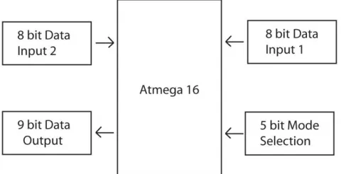
[image:1.612.49.289.455.578.2]In this project we have implemented most of the digital logic operations by atmega16 micro controller. Using 32GPIO pins of atmega16 all the gate level operations and other digital logic operations can be executed. This atmega16 micro controller is preprogrammed and can perform AND, OR, NOR, NAND, XOR, XNOR, Universal Shift Register, Counter etc. operations. Most of the operations are 8bit but few operations are 16bit. Designer just needs to select the operation he wants to execute.
Figure 1:- Basic Project Outline
A. Project Outline
A brief Introduction to internal architecture of microcontroller.
An over view of programming of micro controller.
An over view of Digital logic design gates and registers.
An over view of interface of switches, LEDs.
B. Interfaces Used
Micro controller interface.
Toggle switches interface.
LEDs interface.
C. Software Used
Compiler-MikroC pro AVR version 5.
Simulator- Proteous VSM version 7.8.
II. CIRCUIT DESCRIPTION
International Journal of Emerging Technology and Advanced Engineering
Website: www.ijetae.com (ISSN 2250-2459, ISO 9001:2008 Certified Journal, Volume 3, Issue 6, June 2013)
35
A. Main Technology Used
The main technology of this IC is programming. In different mode we have created different operations. For example if the mode is 00 selected means value from D0 to D4 all are 0. Here D0 is LSB and D4 is MSB bit. Adder operation gets selected. Now PORTC is the first input where C0 bit is LSB and C7 bit is MSB. PORTA is used as second input where A0 is LSB and A7 is MSB. For adder operation code is as following
If((PIND==0x00)||(PIND==0x80)) {ADD=PINC+PINA;
PORTB=ADD;
PORTD7_BIT=Hi(ADD); }
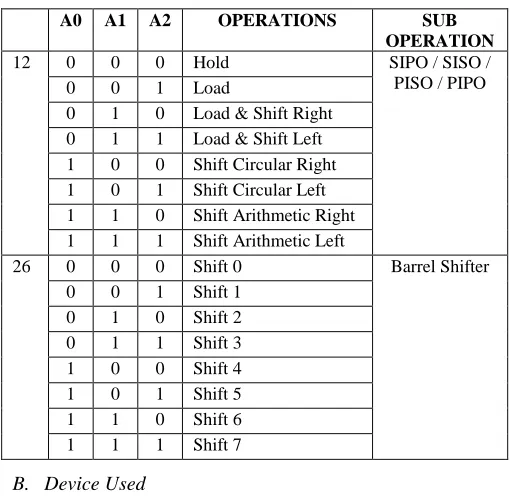
So, for any combination of input1 or input2 this IC will add them and show the output with carry bit. In these way 28 operations has been set. Some operations have sub operations also. Our 12th operation is Universal Shift Register. In order to use this IC we have to select 12th operation at first means D4=0, D3=1, D2=1 & D0=0. Under Universal shift register there are also 4 modes. They are Serial In Parallel Out (SIPO), Serial In Serial Out (SISO), Parallel In Serial Out (PISO) and Parallel In Parallel Out (PIPO). To select SIPO we have to select A6 & A7 bit as 0. Then we have to select which type of shifting we want. If we want to shift left then we have to select A0=0, A1=1, A2=1.
International Journal of Emerging Technology and Advanced Engineering
Website: www.ijetae.com (ISSN 2250-2459, ISO 9001:2008 Certified Journal, Volume 3, Issue 6, June 2013)
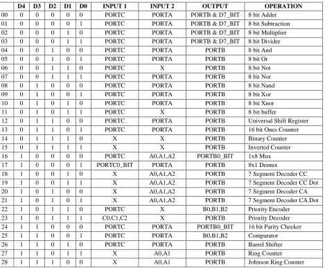
[image:3.612.75.544.159.546.2]36 TABLE I MAIN OPERATION CHART
This Table shows the 28 operation can be done by this micro-controller only by selecting the modes. From this table we can see that Adder, Subtraction, Multiplier & Divider need 2 data inputs and 9bit output. But other operations like And, Or, Nand, Xor, Xnor need two data inputs and output is only 8bit. For 8 bit buffer whatever we give input in PORTC we get the same value in PORTB as output. In 16bit Ones counter mode this IC sum the number of 1 in input data and output the added number in binary format in PORTB. Binary Counter gives the output of 1,2,3,4... up to 2048 in binary format.
It increases it’s counting with each clock. Inverted counter means the 1’s will be 0 and 0’s will be 1 while counting operation is going on.
7 Segment Decoder takes input as binary value and gives output for common cathode without dot, common cathode with dot, common anode without dot and common anode with dot. For example if A0=1, A1=1, A2=0 then seven segment with show 3 as output.
The table below shows sub operations.
D4 D3 D2 D1 D0 INPUT 1 INPUT 2 OUTPUT OPERATION
00 0 0 0 0 0 PORTC PORTA PORTB & D7_BIT 8 bit Adder
01 0 0 0 0 1 PORTC PORTA PORTB & D7_BIT 8 bit Subtraction
02 0 0 0 1 0 PORTC PORTA PORTB & D7_BIT 8 bit Multiplier
03 0 0 0 1 1 PORTC PORTA PORTB & D7_BIT 8 bit Divider
04 0 0 1 0 0 PORTC PORTA PORTB 8 bit And
05 0 0 1 0 1 PORTC PORTA PORTB 8 bit Or
06 0 0 1 1 0 PORTC X PORTB 8 bit Not
07 0 0 1 1 1 PORTC PORTA PORTB 8 bit Nor
08 0 1 0 0 0 PORTC PORTA PORTB 8 bit Nand
09 0 1 0 0 1 PORTC PORTA PORTB 8 bit Xor
10 0 1 0 1 0 PORTC PORTA PORTB 8 bit Xnor
11 0 1 0 1 1 PORTC X PORTB 8 bit buffer
12 0 1 1 0 0 PORTC PORTA PORTB Universal Shift Register
13 0 1 1 0 1 PORTC PORTA PORTB 16 bit Ones Counter
14 0 1 1 1 0 X X PORTB Binary Counter
15 0 1 1 1 1 X X PORTB Inverted Counter
16 1 0 0 0 0 PORTC A0,A1,A2 PORTB0_BIT 1x8 Mux
17 1 0 0 0 1 PORTC0_BIT PORTA PORTB 8x1 Demux
18 1 0 0 1 0 X A0,A1,A2 PORTB 7 Segment Decoder CC
19 1 0 0 1 1 X A0,A1,A2 PORTB 7 Segment Decoder CC Dot
20 1 0 1 0 0 X A0,A1,A2 PORTB 7 Segment Decoder CA
21 1 0 1 0 1 X A0,A1,A2 PORTB 7 Segment Decoder CA Dot
22 1 0 1 1 0 PORTC X B0,B1,B2 Priority Encoder
23 1 0 1 1 1 C0,C1,C2 X PORTB Priority Decoder
24 1 1 0 0 0 PORTC PORTA PORTB0_BIT 16 bit Parity Checker
25 1 1 0 0 1 PORTC PORTA B0,B1,B2 Comparator
26 1 1 0 1 0 PORTC PORTA PORTB Barrel Shifter
27 1 1 0 1 1 X A0,A1 PORTB Ring Counter
International Journal of Emerging Technology and Advanced Engineering
Website: www.ijetae.com (ISSN 2250-2459, ISO 9001:2008 Certified Journal, Volume 3, Issue 6, June 2013)
[image:4.612.381.528.147.325.2]37 TABLE II
SUB OPERATION CHART
TABLE III
COMMANDS OF SUB OPERATION CHART
B. Device Used
Brain of this project is Atmega16 micro-controller. It is a 8 bit Micro controller with RISC architecture. Its speed is up to 16MIPS throughput at 16MHz. It has 16K bytes of flash and 512bytes EEPROM. Operating voltage 2.7v -5.5v, in active mode it consumes only 1.1mA & in sleep mode it consumes less than 1uA current. It has 32GPIO, PWM, SPI, UART, I2C and other features which made it a perfect choice of designing a versatile digital design IC.
[image:4.612.41.297.164.317.2]
Figure 3:- Atmega16 Microcontroller
Our program contains only 10k bytes of flash memory. Still 6k bytes of memory are free for developing other operations.
In our circuit we have used a switch and placed a reset circuit. So reset button can be used to reset the micro controller.
III. TEST RESULTS
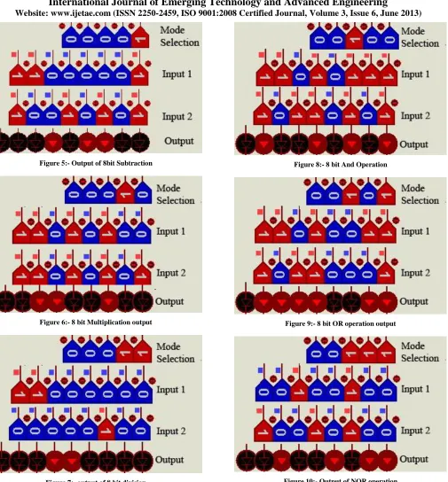
We have performed all the 28 operations and output result was as expected. Bellow we have shown some of the outputs of different operations for different inputs.
Figure 4:- 8bit Adder operation
A7 A6 A5 SUB MAIN
OPERATION 12 0 0 X Serial In Parallel Out Universal Shift
Register 0 1 X Serial In Serial Out
1 0 X Parallel In Serial Out 1 1 X Parallel In Parallel Out
26 0 0 0 Shift Right Logic Barrel Shifter 0 0 1 Shift Right Arithmetic
0 1 X Rotate Right 1 0 0 Shift Left Logic 1 0 1 Shift Left Arithmetic 1 1 X Rotate Left
A0 A1 A2 OPERATIONS SUB
OPERATION
12 0 0 0 Hold SIPO / SISO /
PISO / PIPO
0 0 1 Load
0 1 0 Load & Shift Right 0 1 1 Load & Shift Left 1 0 0 Shift Circular Right 1 0 1 Shift Circular Left 1 1 0 Shift Arithmetic Right 1 1 1 Shift Arithmetic Left
26 0 0 0 Shift 0 Barrel Shifter
[image:4.612.42.297.344.593.2] [image:4.612.324.566.485.641.2]International Journal of Emerging Technology and Advanced Engineering
Website: www.ijetae.com (ISSN 2250-2459, ISO 9001:2008 Certified Journal, Volume 3, Issue 6, June 2013)
[image:5.612.60.565.110.654.2]38 Figure 5:- Output of 8bit Subtraction
Figure 6:- 8 bit Multiplication output
Figure 7:- output of 8 bit division
[image:5.612.55.322.124.643.2]
Figure 8:- 8 bit And Operation
Figure 9:- 8 bit OR operation output
[image:5.612.321.567.126.638.2]International Journal of Emerging Technology and Advanced Engineering
Website: www.ijetae.com (ISSN 2250-2459, ISO 9001:2008 Certified Journal, Volume 3, Issue 6, June 2013)
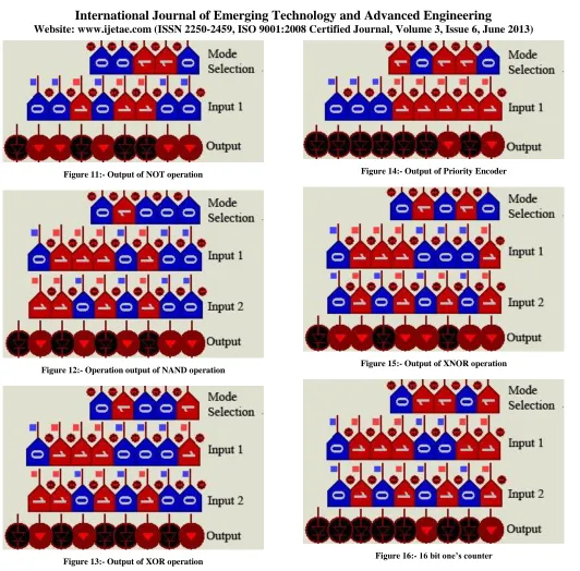
[image:6.612.46.578.98.622.2]39 Figure 11:- Output of NOT operation
Figure 12:- Operation output of NAND operation
Figure 13:- Output of XOR operation
Figure 14:- Output of Priority Encoder
Figure 15:- Output of XNOR operation
[image:6.612.49.290.128.427.2]International Journal of Emerging Technology and Advanced Engineering
Website: www.ijetae.com (ISSN 2250-2459, ISO 9001:2008 Certified Journal, Volume 3, Issue 6, June 2013)
[image:7.612.268.561.102.648.2]40 Figure 17:- 1x8 MUX operation
Figure 18:- 8x1 DEMUX operation
Figure 19:- 7 Segment Decoder Common Cathode
Figure 20:- 16 bit Parity Checker
Figure 21:- 8 bit Comparator
Figure 22:- 8 bit Priority Decoder
IV. FURTHER APPLICATIONS
This IC can be used in many complex Digital design systems. [image:7.612.62.410.110.663.2]International Journal of Emerging Technology and Advanced Engineering
Website: www.ijetae.com (ISSN 2250-2459, ISO 9001:2008 Certified Journal, Volume 3, Issue 6, June 2013)
41
This IC can be used where costly digital logic designlab can’t be set up for education purpose.
Rapid prototype for teaching Digital Logic Design.REFERENCES
[1] Stanisavljevic, Z.; Pavlovic, V. ; Nikolic, B. ; Djordjevic, J.,” SDLDS- System for Digital Logic Design & Simulation”, Education, IEEE Transactions on (Volume:56 , Issue: 2 ), May 2013.
[2] Zemva, A. ; Trost, A. ; Zajc, B.”A Rapid Prototyping Environment for teaching Digital Logic Design”, Education, IEEE Transactions on (Volume:41 , Issue: 4 ), Nov 1998.
[3] Digital design principles and practices by John F. Wakerly.
[4] http://www.electronics-tutorials.ws/sequential/seq_5.html for details
operation of Shift Register.
[5]
http://tams-www.informatik.uni-
hamburg.de/applets/hades/webdemos/20-arithmetic/10-adders/halfadd-fulladd.html for lots of digital design simulation verification.
[6] Guillermo A. Vera, Jorge Parra, Craig Kief, Marios Pattichis and Ho
ward Pollard,” Integrating Reconfigurable Logic in the First Digital
Logic Course”,9th International Conference on Engineering
Education,july 23-28 2006.
[7] Poulastya Mukherjee. Remote Control of Industrial Machines Using
Mobile Phone. IJETAE, Volume 3, Issue 1, January 2013 for project outline diagram.
[8] Atmega16 datasheet by Atmel.
[9] www.mikroe.com for free demo compiler and help of compiler
software.
[10] http://www.labcenter.com/products/vsm/vsm_overview.cfm for
simulator and demo videos of simulation.
AUTHORS PROFILE
Md. Khaled Hossain, is a Lecturer in U-ingenieria on Micro-controller & Embedded System Design. He has Completed BSc. in Electrical & Electronic Engineering from American International University- Bangladesh. His research interests are robotics, automation, control system and embedded system designing. Email: - [email protected].
Md. Nasimuzzaman Chowdhury is doing MSc. in Electrical & Electronic Engineering at American International University-Bangladesh. He has Completed BSc. in Electrical & Electronics Engineering from American International University-Bangladesh. His research interests are- Laser, Wireless Systems, Microwave propagation, Antenna and automation. E-mail:- [email protected]