3 item/ 4 Pi Computers- System/ 4 Pi Computers- System/ 4 Pi Computers- System/4 Pi Computers 3 'tem/4 Pi Computers,"" System/ 4 Pi Computers - System/ 4 Pi Computers - System/4 Pi Computers 3ystem/ 4 Pi Computers - System/4 Pi Computers - System/4 Pi Computers - System/4 Pi Computers
,
"I
item/4 Pi Computers - System/4 Pi Computers - System/4 Pi Computers - System/4 Pi Computers , 'tem/ 4 Pi Computers - System/ 4 Pi Computers - System/4 Pi Computers - System/4 Pi Computers ,ystem/ 4 Pi Computers - System/ 4 Pi Computers-- System/4 Pi Computers - System/ 4 Pi Computers ,~ ;tem/ 4 Pi COl:nputers - System/4 Pi Computers - System/4 Pi Computers- System/4 Pi Computers '.d tem/ 4 Pi Computers - System/4 Pi Computers - System/4 Pi Computers - System/4 Pi Computers 3ystem/ 4 Pi Computers - System/ 4 Pi Computers - System/4 Pi Computers - System/ 4 Pi Computers ::> item/ 4 Pi Computers - System/4 Pi Computers - System/4 Pi Computers - System/ 4 Pi Computers , ·tem/4 Pi Computers - System/ 4 Pi Computers - System/4 Pi Computer-s - System/ 4 Pi Computers ::>ystem/ 4 Pi Computers - System/4 Pi Computers - System/4 Pi Computers - System/4 Pi Computers 3 item/4 Pi Computers - System/4 Pi Computers - System/4 Pi Computers - System/4 Pi Computers 3 t em/4 Pi Computers - System/ 4 Pi Computers - System/4 Pi Computers - System/4 Pi Computers 3ystem/4 Pi Computers - System/4 Pi Computers - System/ 4 Pi Computers - System/4 Pi Computers S~ .tem/4 Pi Computers - System/ 4 Pi Computers - System/4 Pi Computers - System/ 4 Pi Computers S,Jio.Jtem/ 4 Pi Computers - System/4 Pi Computers - System/4 Pi Computers - System/4 Pi computes System/4 Pi Computers - System/ 4 Pi Compute,rs - System/4 Pi Computers - System/4 Pi Compute S,- item/ 4 Pi Computers - System/ 4 Pi Computers - System/4 Pi Computers - System/4 Pi Compute S tem/ 4 Pi Computers - System/4 Pi Computers - System/4pi
Computers - System/4 Pi rs System/ 4 Pi Computers - System/ 4 Pi Computers - System/4 Pi Computers - SysteS,-item/ 4 Pi Computers - System/ 4 Pi Computers - System/4 Pi ' SJ-item/ 4 Pi Computers - System/ 4 Pi Computers - System/4
System/ 4 Pi Computers - System/ 4 Pi Computers - System/4
S rtem/ 4 Pi Computers - System/ 4 Pi Compu - ystem/4 P rs
S_ 'tem/ 4 Pi Computers - System/ 4 Pi ystem/4 Pi Pi Computers
System/ 4 Pi Computers - System/ ystem/4 Pi Com Pi Computers
S :tem/ 4 Pi Computers - / i Co - ystem/ 4 Pi , Pi ~omputer
S t em/ 4 Pi Compu
-i$
Ss em 4 . C stem/4 Pi - System/ 4 Pi ComputersSystem/ 4 Pi - s m 4 P Co S rri/ 4 Pi Computers - System/ 4 Pi Computer ~ S item/ 4 Co ter - S Pi 0 p e s Sy - m/4 Pi Computers - s1tem/ 4 Pi Computer
SJ,.-ltem/ 4 P m uters SY~4 om ut s - ystem/4 Pi Sys /4 Pi Computer
System/4 Pi C m ters Sy el 4 0 ters - System/4 Pi 4 Pi Computers S~ item/ 4 Pi Co p ers - y8 em/ i ompute s - Syste Pi Pi Computers
S tem/4 Pi Co pu S 4 Pi Co - Syste 4 Pi Computers
System/4 Pi C pute - ystem/ 4 Pi Com s - Sys Pi Computer"
S item/ 4 Pi Co ers - System/ 4 Pi Co s - Sy s - Syste Pi Computers
S ·tem! 4 Pi Computers - System/4 Pi Co _ - System/ 4 Pi Computers
System/ 4 Pi Computers - System/4 Pi s - System/ 4 Pi Computers
S, item/4 Pi Computers - Sy Pi Co s - Sy em/4 omputers - System/ 4 Pi Computers
S -tem/ 4 Pi Compute - System/4 Pi Computers - System/4 Pi Computers System/4 Pi Co - System/4 Pi Computers - System/4 Pi Computers
;tem/ s - System/4 Pi Computers - System/4 Pi Computers
rs - System/4 Pi Computers - System/4 Pi Computers Compu rs - System/4 Pi Computers - System/4 Pi Computers
em/4 Pi Computers - System/ 4 Pi Computers - System/4 Pi Computers
s - System/ 4 PI Computers - System/4 Pi -Computers - System/4 Pi Computers
rs - System/4 Pi Computers - System/4 Pi"Computers - System/4 Pi-Computers
4 Pi Computers - System/4 Pi Computers - System/ 4 PI Computers - System/4 Pi Computers
S -tem/4 Pi Computers - System/ 4 Pi Computers - System/ 4 Pi Computers - System/4 Pi Computers
System/4 Pi Computers - System/ 4 Pi Computers - System/4 Pi Computers - System/4 Pi Computers
S' item/ 4 Pi Computers - System:; 4 Pi Computers - System/4 Pi Con1puters - System/4 Pi Computers
Technical Description of
IBM System/4 Pi Computers
This data shall not be disclosed outside the recipient or the Government or be duplicated, used or disclosed in whole or in part for any other purpose other than to evaluate this data; provided, that if a contract is a warded to IDM as a re-sult of, or in connection with, the submission of such data, the recipient or the Government shall have the right to du-plicate, use or disclose this data to the extent provided in the contract. This restriction does not limit the recipient's or the Government's right to use information contained in such data if it is obtained from another source.
TABLE OF CONTENTS
Section Title
1 SYSTEM/4PiSUMMARY . . . 0 0 0 0 0 0 . 0 0 0 0 0 0 0 0 1-1
INTRODUCTION 0 0 0 0 0 0 0 0 0 0 0 0 0 0 0 0 • 0 0 0 0 0 0 0 0 1-3
TECHNOLOGY 0 0 0 0 0 0 0 0 • • • 0 0 0 0 0 0 • 0 • 0 0 0 0 0 0 1-5
Circuits 0 0 • 0 0 0 0 0 0 0 0 0 0 0 0 0 0 0 0 • 0 0 0 0 0 0 0 0 1-5
Multilayer Interconnection Boards o. 0 0 0 0 0 0 0 0 1-5
Main Stor age 0 0 0 • 0 0 0 0 • 0 0 0 0 0 0 0 0 0 0 0 0 0 0 • 0 1-7
Read Only Storage 0 0 0 0 0 0 • 0 0 0 0 0 • 0 • 0 • 0 0 0 0 1-7
MANUFACTURtNG TEST DATA SYSTEM ••••• 0 • • • 1-10
SlJPPORT PROGRAMMING SYSTEM. • • • • • • • • • •• 1-10
2 MODEL TC (TACTICAL COMPUTER) . 0 0 0 • • • 0 0 • • 0 o. 2-1
SUMMARY .• 0 0 0 0 0 0 0 0 0 0 • • 0 0 • • 0 • 0 0 • • • • 0 • • 2-3
DATA AND INSTRUCTION FORMATS . • . 0 0 0 • • • • • 2-3
ADDRESSING . 0 0 • 0 • 0 • • 0 0 • 0 0 0 0 • • 0 0 • 0 0 • • • • 2-5
PROCESSOR ORGANIZATION . 0 0 0 • 0 0 0 0 • • • • 0 • 0 2-6
MAIN STORAGE
INPUT/OUTPUT
2-7
2-7
PHYSICAL CHARACTERISTIC~ 0 0 • • 0 • 0 0 • • • • • • 0 2-8
INSTRUCTIONS 0 0 0 • 0 • 0 • 0 0 0 • 0 0 0 0 • 0 0 0 0 0 • 0 0 0 2-9
3 MODEL CP (CUSTOMIZED PROCESSOR) 0 • • • • 0 0 0 • 0 • • 3-1
SUMMARY . 0 • • • 0 0 • 0 • • 0 • • • 0 0 0 0 • • 0 0 • 0 • •
o.
3-3Section
3
TABLE OF CONTENTS (Cont)
Title Page
ADDRESSING .. . . . • . . . . . 3-6
PROCESSOR ORGANIZATION . . . 3-6
INPUT/OUTPUT . . . .. 3-7
PHYSICAL CHARACTERISTICS . . . .. 3-7
INSTRUCTIONS. . . .. 3-7
4 MODEL EP (EXTENDED PERFORMANCE) . . . 4-1
SUMMARY . . . . . 4-3
DATA AND INSTRUCTION FORMATS . . . . . 4-3
ADDRESSING . . . . . . • . . . . .• 4-6
PROCESSOR ORGANIZATION . • . • . • • • • • • . • . . • 4-7
INP UT / 0 UTP UT . • • • • . . . • • . • . . . • . . . • . . • .• 4 - 8
PHYSICAL CHARACTERISTICS . . . • • • . • • . . . . •. 4-9
FOREWORD
The Federal Systems Division of IBM has developed a family of general-purpose, militarized, digital computers called System/4 Pi. The name 4 Pi refers to the number of steradians in a sphere. It symbolizes System/4 Pi's general-purpose adaptability to the entire spectrum of military and space applications.
Section 1
...
I
INTRODUCTION
When IBM began its System/4 Pi development program early in 1965, the following gUidelines were established:
• Only proven technologies and proven manufacturing techniques would be considered.
• Maximum commonality with IBM's commercial technology would be maintained to insure that the resources of the entire IBM Corpora-tion would be available.
• An off-the-shelf production capability would be developed so that reliable systems could be produced in large quantities with mini-mum lead time.
• The design of each computer would be general-purpose, so that each computer model could address a wide range of military and space applications.
Adhering to those gUidelines, a computer engineering team designed and developed a family of computers that consists of three basic models:
• Model TC (Tactical Computer) - A briefcase-size computer for applications such as missile gUidance, helicopters, satellites and submarinest>
• Model CP (Customized Processor) - An intermediate-range processor for applications such as aircraft navigation, weapons delivery, radar correlation and mobile battlefield systems. • Model EP (Extended Performance) .- A large-scale data
proc-essor for applications requiring real-time processing of large volumes of data, such as manned spacecraft, airborne warning and control systems and command and control systems.
In 1966, System/4 Pi computers were selected for four major military programs with a current contract value to IBM of more than $50 million. Deliveries began in March 1967.
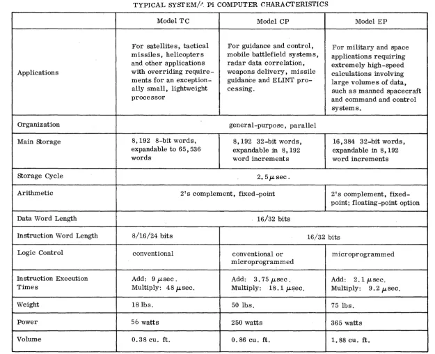
Table 1-1
TYPICAL SYSTEM/,A. Pi COMPUTER CHARACTERISTICS
Model TC Model CP Model EP
For satellites, tactical For gu~dance and control, For military and space
missiles, helicopters mobile battlefield systems, applications requiring
and other applications radar data correlation, extremely high-speed
Applications with overriding require- weapons delivery, missile calculations involving
ments for an exception- guidance and ELINT pro- large volumes of data,
ally small, lightweight cessing. such as manned spacecraft
processor and command and control
systems.
Organization general-purpose, parallel
Main storage 8,192 8-bit words, 8,192 32-bit words, 16,384 32-bit words,
expandable to 65,536 expandable in 8,192 expandable in 8, 192
words word increments word increments
storage Cycle 2.5 J-L sec.
Arithmetic 2' s complement, fixed-point 2's complement,
fixed-point; floating-point option
Data Word Length 16/32 bits
Instruction Word Length 8/16/24 bits 16/32 bits
Logic Control conventional conventional or m icroprogramm ed
microprogrammed
Instruction Execution Add: 9 p-sec . Add: 3.75 fLsec. Add: 2.1 J-Lsec.
Times Multiply: 48 fLsec. Multiply: 18.1 J-Llf?ec. Multiply: 9.2 J-Lsec.
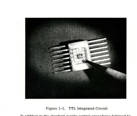
[image:10.795.70.696.65.573.2]TECHNOLOGY
Circuits
Transistor -transistor logic (TTL) integrated circuits are used in all System/4 Pi computers. The circuits are currently available from several manufacturers.
Figure 1-1. TTL Integrated Circuit
In addition to the standard quality control procedures followed by circuit manufacturers, IBM subjects the circuits to its own stringent quality screening. IBM's evaluation includes 100 per cent inspection, burn-in and acceleration/vibration testing. Complete failure analysis data is compiled and used in a reliability improvement program.
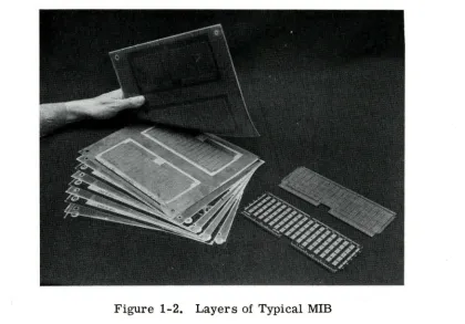
Multilayer Interconnection Boards
[image:11.612.63.507.163.539.2]Figure 1-2. Layers of Typical MIB
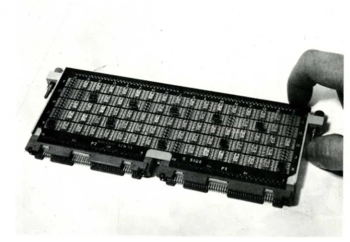
Integrated circuits and discrete components are soldered to etched patterns on the surface of a MIB. Plated-through holes interconnect MIB layers. Feed-through holes are provided at the top of each MIB for inter-connection between MIBs on each side of the metal frame. Figure 1-3 shows a typical page with integrated circuit flatpacks and discrete components.
The pages of a subassembly are interconnected by a MIB backpanel. Page connectors were developed by IBM for the Sa,turn V Launch Vehicle Digital Computer. The connectors are fully qualified and their reliability
nas been demonstrated.
[image:12.611.108.528.144.437.2]Figure 1-3. System/4 Pi Page
Main Storage
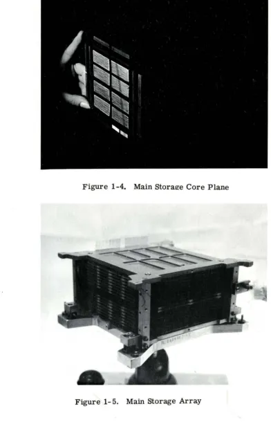
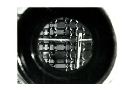
System/4 Pi main storage arrays are assembled from core planes that are militarized versions of those used in IBM System/360 computers. (See
Figure 1-4.) The core material used for ,System/4 Pi is lithium-nickel
fer-rite, which maintains its magnetic properties over a wide temperature range.
Core dimensions, are O. 013-inch inner diameter and O. 021-inch outer
diameter. Each core plane contains 16, 896 cores, which are automatically wired and tested. The basic storage module has 18 core planes stacked into an array. A conformal coating is applied to the planes for environmental protection of cores, and form padding is placed between planes to further ruggedize the array. Figure 1-5 shows a standard 4 Pi array.
The basic storage module contains 8, 192 32- bit words. An additional 256 words are contained in the module, but those are usually reserved for I/O control purposes and are not addressable by the programmer. Additional
8, 192-word modules may be added on a plug-in basis.
Read- Only Storage
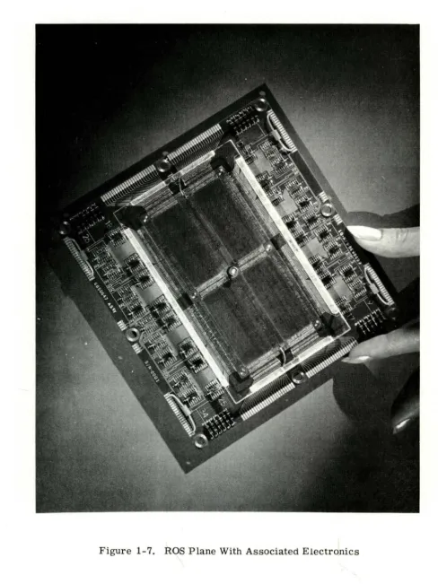
In certain configurations of System/4 Pi, the computer control is
implemented by microprograms contained in a read-only storage maS)
[image:13.614.119.472.108.351.2]Figure 1-4. Main Storae:e Core Plane
[image:14.617.152.486.104.354.2] [image:14.617.102.494.115.728.2]the selection of paths for data flow, the opening and closing of gates and registers, sequencing of events and all other functions to implement a logical operation or to effect a data transfer.
Unlike conventionally controlled computers, in which computer states have traditionally been stored in elements such as flip-flops, sequence trig-gers and latches, a microprogrammed processor's computer states are stored discretely in program-like form. When an instruction is read from main storage, the operation code portion specifies a starting address of a microroutine in ROS that will perform the step-by-step execution of the instruction. Every instruction in the computer's repertoire is microp ro-grammed and executed as a group of microinstructions in ROS.
In System/4 Pi, the ROS microprogrammed control is implemented with magnetic cores O. 007-inch inner diameter and O. 012-inch outer diam-eter. The cores are automatically wired into a word- organized array. A missing-core technique is used to form bit patterns and to implement the read-only function. A core at the intersection of two wires indicates a logical one, while the absence of a core indicates a logical zero.
[image:15.611.85.496.374.669.2]ROS core planes are mounted on a MIB containing flatpack drive and sense circuits. Figure 1-7 shows a ROS plane and its associated electronics.
The primary advantage of a ROS-controlled computer is adaptability to special applications. Special microroutines, or application-oriented instruc-tions, may be incorporated into the computer without hardware redesign. Iterative routines can often be executed ten times faster by implementing a ROS micro routine to replace a subroutine that is executed from main storage. This results in considerable savings of main storage locations. Since ROS is a pluggable unit, a user can defer selecting the exact instruction set for his particular application. When the problem to be solved is completely defined, an instruction set can be chosen that will customize the computer to the application.
ROS is expandable from 1,024 to 3, 072 words, 70 or 100 bits in length. System/4 Pi Model EP is controlled by ROS, while ROS is offered as an op-tion in Model CPo
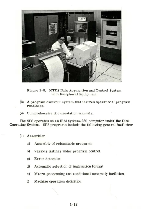
MANUFACTURING TEST DATA SYSTEM (MTDS)
MTDS is a single hardware and software factory test equipment complex for System/4 Pi hardware. It consists of an IBM 1800 Data Acquisition and Control System (DACS), input/output adapters and peripheral data proc-essing equipment. The 1800 DACS, when coupled to a suitable adapter unit, executes a program that completely tests a subassembly, assembly or final unit.
MTDS provides a unified solution to the problem of factory testing and eliminates the expense of individual manual tests of equipment, insuring high reliability testing at low cost.
MTDS is one of the most automated factory test complexes in existence. It will satisfy the testing requirements of IBM military and space hardware for at least five years.
Figure 1-8 shows the DACS and peripheral data processing equipment. SUPPORT PROGRAMMING SYSTEM (SPS)
The SPS is a comprehensive set of programs for System/4 Pi com-puters. The SPS provides:
(1) Programming aids that enable a program to be expressed in a readily understood language.
Figure 1-8. MTDS Data Acquisition and Control System
with Peripheral Equipment
(3) A program checkout system that insures operational program
readiness.
(4) Comprehensive documentation manuals.
The SPS operates on an IBM System/360 computer under the Disk
Operating System. SPS programs include the follOwing general facilities:
(1) Assembler
a) Assembly of relocatable programs
b) Various listings under program control
c) Error detection
d) Automatic selection of instruction format
e) Macro-processing and conditional assembly facilities
[image:18.611.68.530.68.749.2](2) Service Programs
a) Linkage Editor
• Combines and relocates programs assembled separately
• Resolves program linkages
b) Job Control
• Provides batch processing for handling the transistion from assembly to linkage editing to simulation
c) Library Maintenance and Service
• Maintains the system disk libraries
• Edits user source programs
• Displays or lists library contents
(3) Simulator
a) Dynamic simulation faciltated through control of a user's written FORTRAN program
b) User access to simulated computer object program data (with symbolic reference)
c) Object program correction
d) Program debugging options (dump, snap, trace)
e) Simulation of input/output and interrupt initiation and response.
Section 2 MODELTC
l\.:)
I
l\.:)
SUMMARY
The Model TC (Tactical Computer) is a general-purpose, stored-program, digital computer. It is designed for the low-cost, medium range of computational performance. Hardware requirements are minimized by using a byte (eight-bit) data transfer format and hardware registers to per-form multifunctions.
The computer is subdivided into a storage, processor and 110 section. AU signals entering or leaving the computer are digital in nature. The 2.5-microsecond, 8,192 bytes of core storage have a parallel eight-bit trans-fer path to the processor section and operate within a basic three- microsecond machine cycle. Storage is expandable to 16, 384 bytes without modification.
The processor is organized as a three- bus system with eight-bit paral-lel data flow. The processor contains facilities for addressing main storage; fetching or storing information; performing arithmetic and logical data
processing; sequencing and timing instructions, and initiating communications between storage and external equipment.
Working registers are located in both hardware and storage. Fifty-four instructions are implemented. Processing rates on the order of 50, 000
operations a second are attained by optimizing the machine organization, and by using monolithic logic circuitry and high- speed core storage.
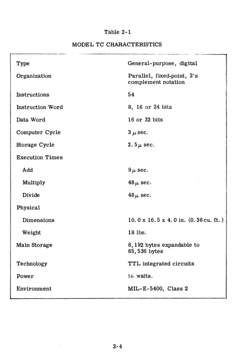
Model TC characteristics are summarized in Table 2-1. DATA AND INSTRUCTION FORMATS
The Model TC has a standard 16-bit data word. A 32-bit data word may be used when double-precision accuracy is required.
Positive numbers are always in true-binary form; negative numbers are in 2' s complement form.
o
15Fraction
o
31Fraction
Type
Organization
Instructions Instruction Word Data Word
Computer Cycle ·Storage Cycle
Execution Times Add
Multiply Divide Physical
Dimensions Weight Main Storage
Technology Power
Environment
Table 2-1
MODEL TC CHARACTERISTICS
General-purpose, digital Parallel, fixed-point, 2' s complement notation 54
8, 16 or 24 bits 16 or 32 bits
3 fL sec.
2. 5fL sec.
9 fL sec.
48fL sec.
48fL sec.
10. 0 x 16. 5 x 4. 0 in. (0. 38 cu. ft. ) 18 lbs.
8,192 bytes expandable to 65, 536 bytes
TTL integrated circuits
56 watts.
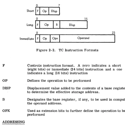
[image:23.620.75.553.63.764.2]F
OP
DISP
B
OPX
The instruction words in the Model TC are 8, 16 or 24 bits long.
0 7
Short
I
FI
OpI
DispI
0 15
Long
I
F
I
OpI
BI
DispI
0 23
Immediate
I
FI
OpI
OpxI
OperandFigure 2-2. TC Instruction Formats
Controls instruction format. A zero indicates a short (eight bits) or immediate (24 bits) instruction and a one indicate s a long (16 bits) instruction
Defines the operation to be performed
Displacement value added to the contents of a base register to determine the effective storage address.
Designates the base register, if any, to be used in computing the operand address.
Used as extension bits to further define the operation to be performed
ADDRESSING
[image:24.621.86.498.171.593.2]bytes, using a 16-bit binary address. Some main storage locations are re-served for special purposes.
For addressing purposes, operands can be grouped in two classes: (1) explicitly addressed operands and (2) immediate operands placed as part of the instruction stream.
To permit the ready relocation of program segments and to provide for flexible specifications on input, output and working areas, all instructions referring to main storage employ a full storage address. The address used to refer to main storage is generated as follows:
Base Address (B) is a 16-bit number contained in one of three storage registers specified in the B-field of the long format instruction. Base register one is implied when computing operand addresses for short format instructions. The base address can be used as a means of static relocation of programs and data. The base address provides addressing for the entire main storage. A special base register, designated link-age register (L), may be used to store the instruction counter for sub-routine linking.
Displacement (DISP) is binary number contained in the instruction for-mats. It is included as part of every address computation. The dis-placement provides relative addressing for up to 256 syllables (16-bit words) for long-format instructions and 16 syllables for short-format instructions.
In forming the address, the contents of the base register are treated as an -unsigned 16-bit positive binary integer. The displacement is similarly treated as a positive binary integer. The two are added as 16-bit binary num-bers, ignoring overflow. The resulting sum is the effective address of the left-most byte of the operand.
PROCESSOR ORGANIZATION
The data flow within the processor section is via one of three data buses: X, Y or main. The X-bus gates one of eight registers to the left side of the adder. The Y-bus gates one of three registers to the right side of the adder. Output data from the adder is distributed to anyone of seven registers via the main bus. Data inputs and outputs to and from the 110 are transferred via the main bus.
The hardware registers in the processor section are also packaged with two bits contained in each flatpack, without the requirement for external gating hardware.
The interrupt system implemented in the Model TC permits a change in the state of the computer in response to conditions external to the system. Three external interrupt lines are provided.
The occurrence of an interrupt sets a bit in the interrupt level status register (ILSR) and forces an instruction to Branch and Store Instruction Counter. The instruction counter is stored in a location permanently as-signed to the interrupt. The interrupt handling routine reads the ILSR to de-termine the source of the interrupt and proceeds with the required processing.
The priority assigned to the interrupts is under program control. Interrupts are automatically masked during interrupt processing. Interrupts are unmasked under program control by the Load Status Word instruction, which resets the interrupt inhibit latch.
MAIN STORAGE
The Model TC uses an 8, 192-word by eight-bit core storage with a 2.5-microsecond cycle time. The access time is O. 9 microseconds. A coincident-current (3D) selection scheme is used. The storage array requires four core planes. Figure 2- 3 shows a Model TC main storage array. The operating ambient temperature range is -550C to +100oC.
The monolithic circuits used in the main storage assembly are designed within state-of-the-art ground rules obtained from integrated circuit manu-facturers. The high-voltage, high-current address driver and inhibit driver
consist of monolithic pre-driver transformers coupled to discrete chip out-put stages packaged in flatpacks. The sense amplifier is a monolithic circuit with external networks for threshold setting.
INPUT/OUTPUT
.The I/O section of the Model TC performs the following functions: • Data Transfers. - A serial data channel is implemented which
l
/
Figure 2-3. TC Main Storage Array
• Device Address Generation - Individual devices sharing the data channel are controlled by 11 address lines decoded from the ad-dress field of the laC instruction word.
• Interrupt Control - All interrupts are buffered by a three-bit register. When an interrupt occurs, the corresponding bit is set and remains pending until the processor services the interrupt. Interrupts provide the only means of external interrogation of the computer.
• Real Time Clock - The
I/o
section contains a 24-bit real-time counter, driven at a 333-kilohertz bit rate by the computer clock.The 16 high order bits of the 24-bit counter are read by the computer under program control. The low-order bit of the 16 bits changes state every 768 microseconds. The full range of the counter is in excess of 50 seconds.
PHYSICAL CHARACTERISTICS
[image:27.617.64.559.85.753.2]Electrical interfacing is accomplished with four input/output connec-tors on the front panel. Lightweight magnesium covers at the top and back of the unit facilitate removal of the subassemblies, provide radio frequency attenuation and prevent the entrance of foreign materials.
The computer is designed to meet the requirements of MIL-E-5400, Class 2. The three subassemblies are all of the same basic construction, differing only in the type of electronic components.
Each subassembly (page) consists of two MIBs, a thermal mounting plate, I/O connectors and circuit components.
The processor page (Figure 2-4) contains all the logic circuitry of the computer. It consists of two Mills on which transistor-transistor logic (TTL) integrated circuit flatpacks are soldered. Between the MIBs is a metal
supporting structure and three 98-pin connectors. An insulator separates each MIB from the supporting structure. Feed-throughs are provided to allow electrical connection between the two MIBs of the page. Each MIB contains two levels of signal wires and two internal ground-voltage planes.
The I/O page is identical in design to the processor page. The timing and operational I/O is packaged on one side of the page and the logic for a portable storage loader is packaged on the other side.
The main storage page (Figure 2-5) contains an 8,192 by eight-bit storage array mounted on the underside. The drive and sense circuits are mounted on top of the page.
The storage array consists of the following subdivisions: • Four core planes
• Two diode printed circuit boards • Three re sistor termination boards • One X-line jumper board
INSTRUCTIONS
Figu,.e 2-5. Main Storage Page
Table 2-2
MODEL TC INSTRUCTION LIST
.,---
... . .. _.-_ ...•. _ •... _
-Operation ADD ADD ADD
ADD DOUBLE AND
AND
ARITHMETIC COMPLEMENT BRANCH
BRANCH
BRANCH BACKWARD ON MINUS BRANCH BACKWARD ON PLUS BRANCH BACKWARD
UNCONDITIONAL
BRANCH BACKWARD ON ZERO BRANCH FORWARD ON MINUS BRANCH FORWARD ON PLUS BRANCH FORWARD
UNCONDITIONAL
BRANCH FORWARD ON ZERO BRANCH INDffiECT
BRANCH INDffiECT & STORE IC COMPARE
COMPARE
COMPARE DOUBLE DIVIDE
EXCHANGE A & Q EXCLUSIVE OR
INPUT/OUTPUT CONTROL LOAD A
LOAD A LOAD A LOAD BASE LOAD BASE 1 LOAD BASE 2 LOAD BASE 3 LOAD DOUBLE
Format Short Long Immediate Long Immediate Long Short Immediate Long Long Long Long Long Long Long Long Long Long Long Immediate Long Long Long Short Long Long Short Long Immediate Long Immediate Immediate Immediate Long
*Execution time is 6 J-L sec less if B=OO.
I.
[image:31.615.91.529.94.716.2]Table 2-2. Model TC Instruction List (cont.)
Operation
LOAD STATUS WORD MODIFY BASE
MULTIPLY MULTIPLY NO OPERATION OR
SHIFT LEFT DOUBLE SHIFT RIGHT ARITHMETIC
DOUBLE SKIP ON CARRY STORE A
STORE A STORE BASE STORE DOUBLE STORE IC
STORE STATUS WORD SUBTRACT
SUBTRACT
SUBTRACT DOUBLE TALLY ZEROQ Format Long Long Short Long Short Long Short Short Short Short Long Long Long Long Long Short Long Long Long Short
*Execution time is 6 fL sec. less if B=OO.
Execution Time (J.Lsec.)
12 18 51 54* 3 18 6-18 6-18 3 15 18* 18 24* 18 12 15
18*
J
24* 12-24
[image:32.623.91.520.113.446.2]---.-Section 3
MODELCP
SUMMARY
The System/4 Pi Model CP {Customized Processor} is a general-purpose, fixed- point, digital computer. The rugged design and flexible control options satisfy varied applications such as real-time control, radar data correlation, navigation, guidance and weapons delivery.
The computer is subdivided into a central processing unit (CPU), main storage, input/output (I/O), an optional read-only storage (ROS) control and a power supply.
The 2. 5-microsecond main storage contains 8, 192 words, each 36 bits long. Two parity bits and two storage-protect bits are aSSigned to each stor-age word, with the remaining 32 bits forming the standard data word. Main storage is expandable in 8, 192-word increments.
A microprogrammed logic control element, ideally suited to specialized applications, is available as an option with the Model CP. In the micropro-grammed control configuration, each instruction read from main storage is implemented as a short subroutine of microinstructions executed from a ROS device. The movement of data between registers, through the adder, I/O transfers, etc., is completely under the control of microinstructions contained in ROS.
Working registers are located in high- speed hardware. Processing rates on the order of 125,000 operations a second are attained by optimizing the processor organization and by using monolithic logic circuitry and high-speed core storage. Much higher high-speeds are possible for specialized appli-cations by implementing special microroutines and application- oriented instructions in ROS.
Model CP characteristics are summarized in Table 3-1. DATA AND INSTRUCTION FORMATS
The Model CP is implemented with a standard 32- bit data word. A 16-bit halfword can also be used when the fullword accuracy is not required. (See Figure 3-1. )
Type
Organization
Instructions Instruction Word Data Word
Computer Cycle Storage Cycle Execution Times
Add Multiply Divide Physical
Dimensions Weight
Main Storage
Technology Power
Environment
Table 3-1
[image:36.618.75.521.98.717.2]MODEL CP CHARACTERISTICS
... ~.'-"-'.'"-'--.--'.'--'---.-'. , ...
_.
__ .-... .General-purpose, digital
Parallel, fixed point, 2' s complement notation
61 (basic) 16 or 32 bits 16 or 32 bits 417 nsec.
2. 5fL sec.
3. 75fL sec.
18. 13 fL sec. 45. 42fLsec.
10 x 7. 6 x 19.4-in. (0. 86 cu. ft. ) 501bs.
8, 192 x 32-bit words, expandable in 8, 192 word increments
TT L integrated circuits 250 watts
OP
F
T
DISP
I
x
o
15Fraction
o
31Fraction
Figure 3-1. CP Data Formats
The instruction words are 16 or 32 bits long.
0 15
I
OpH
T DispI
0 31
[image:37.620.135.487.75.404.2]I
OpIFI
TII
I
XIOPX,MI
AddressFigure 3-2. CP Instruction Formats The bits within the instruction words are used as follows:
Defines the operation to be performed.
Controls the instruction format. A zero indicates a normal for-mat instruction and a one indicates a long forfor-mat instruction. Tag field addresses the index register or instruction register used in the address modification.
Displacement value added to the instruction register or the index register specified by T to compute the effective address (EA). If T is 00 (normal format only), the displacement is added to the Instruction Register. The displacement is in 2' s complement form if negative, with the sign in bit 8. The bit in position 8 is automatically extended to the higher order bits (0-7) when the displacement is added to an index register. Indirect addressing bit. If zero, addressing will be direct.
If one, addressing will be indirect.
[image:37.620.132.491.126.245.2]OPX,M
ADDRESS
ADDRESSING
Used as operation code extension or modifier, or as specific conditions for branch instructions.
These 16 bits contain the address in a long format instruction.
It can be modified by the contents of an index register or can be an indirect address.
All core storage locations are directly addressable under program con-trol. The effective address may be determined by examining the tag, format and indirect address bits shown in Figure 3-2. The effective address is formed as shown in Table ~-2.
Table 3-2
EFFECTIVE ADDRESS GENERATION
Index Register Relative Address Direct Address Indirect Address
0 Instruction Reg- ADDRESS C (ADDRESS)** ister + DISP*
1 XR1 + DISP ADDRESS + XR1 C (ADDRESS + XR1)
2 XR2 + DISP ADDRESS + XR2 C (ADDRESS + XR2)
3 XR3 + DISP ADDRESS + XR3 C (ADDRESS + XR3)
*DISP may be positive or negative
**C means contents of ADDRESS field in instruction
The recognition of an indirect address control bit in an instruction will cause the address portion to be treated as an indirect address. The address, after indexing (if specified), gives the location of the effective address.
PROCESSOR ORGANIZATION
The interrupt system allows considerable flexibility for the programmer. Several levels of interrupt priority can be assigned. An automatic branch from the normal program sequence is initiated when an interrupt signal is detected. Interrupts are permitted immediately after the completion of an instruction. Each type of interrupt forces a branch to a unique address where the interrupt handling routine is stored. When the interrupt routine is com-pleted' the next lower level interrupt is serviced, or the interrupted program is resumed.
INPUT/OUTPUT
A variety of I/O options are available on the Model CPo High-speed data channels that transfer 16 or 32 bits in parallel can be provided, operat-ing under external or program control. Data rates on the order of 260,000 words a second are possible. In addition, the I/O section can address dis-crete inputs and outputs.
PHYSICAL CHARACTERISTICS
The Model CP is packaged in a dip- brazed aluminum structure. Heat generated from the subassemblies is conducted to the side walls of the struc-ture. The walls consist of a hollow rectangular extrusion which forms a pas-sage for the cooling air. Thin corrugated sheeting is brazed within the paspas-sage to provide the surface area for forced- air convection cooling and to make the structure rigid. The cooling air enters the passage on the rear panel and exits at the front panel.
Lightweight covers at the top and bottom of the unit facilitate removal of subassemblies, provide radio frequency attenuation and prevent entrance of foreign materials.
Operation ADD ADD
ADD HALFWORD ADD HALFWORD AND
AND
Table 3-3
MODEL CP BASIC INSTRUCTION SET Format Normal Long Normal Long Normal Long
Table 3-3. Model CP Basic Instruction Set (cont.)
Operation Format Typical Execution Time (}L sec.
BRANCH ON CONDITION Long 4.58
BRANCH OUT ON CONDITION Long 5.42
BRANCH AND STORE
INSTRUC-TION COUNTER Normal 6.46
BRANCH AND STORE
INSTRUC-TION COUNTER Long 7.71
COMPARE Normal 4.79
COMPARE Long 6.04
COMPARE HALFWORD Normal 3.96
COMPARE HALFWORD Long 5.21
DffiECT INPUT OUTPUT CONTROL Normal 2.50 DffiECT INPUT OUTPUT CONTROL Long 3.75
DIVIDE Normal 47.29
I
DIVIDE Long 48.54EXCLUSIVE OR Normal 3.75
EXCLUSIVE OR Long 5.00
INSERT STORAGE PROTEC T BIT Long 5.42
LOAD A Normal 3.75
LOAD A Long 5.00
LOAD A HALFWORD Normal 3.75
LOAD A HALFWORD Long 5.00
LOAD INDEX Normal 3.75
LOAD INDEX Long 5.00
LOADQ Normal 3.75
LOADQ Long 5.00
LOAD STATUS WORD Long 3.3~
MODIFY INDEX Normal 2.08
MODIFY INDEX Long 3.33
, MODIFY STORAGE HALFWORD Long 5.83
MULTIPLY Normal 18.13
MULTIPLY Long 19.38
MULTIPLY HALFWORD Normal 11. 46
MULTIPLY HALFWORD Long 12.71
OR Normal 3.75
OR Long 5.00
SHIFT LEFT Normal Varies
SHIFT LEFT AND COUNT Normal Varies
SHIFT LEFT AND COUNT
DOUBLE Normal Varies
SHIFT LEFT DOUBLE Normal Varies
SHIFT RIGHT ARITHMETIC Normal Varies
~.
SHIFT RIGHT ARITHMETIC
[image:40.615.83.522.123.704.2]Table 3-3. Model CP Basic Instruction Set cont.
Operation
SHIFT RIGHT LOGICAL
SHIFT RIGHT ROTATE DOUBLE SKIP ON CONDITION
STORE A STORE A
STORE A HALFWORD STORE A HALFWORD STORE INDEX
STORE INDEX STORE Q STORE Q
STORE STATUS WORD SUBTRACT
SUBTRACT
SUBTRACT HALFWORD SUBTRACT HALFWORD
Format Normal Normal Normal Normal Long Normal Long Normal Long Normal Long Long Normal Long Normal Long
Typical Execution Time (j.Lsec.)
[image:41.617.80.534.110.777.2]Section 4
MODEL EP
SUMMARY
The Model EP is a high-performance digital computer with a 32-bit parallel data flow. It features microprogram logic control, which provides flexibility in defining special instructions. Microprograms control data flow, permitting changes to a standard instruction set without changing computer hardware.
The 2. 5-microsecond main storage contains 16,384 words, each 36 bits long. Four parity bits are included in each storage word, with the remaining 32 bits forming the standard data word. Main storage is expandable in 8, 192-word increments.
The input/output section uses an IBM System/360 multiplexer channel augmented by a high- speed interface to handle high data rates. A multiplexer channel provides a flexible and economical means of attaching multiple de-vices to the computer by time-sharing the channel hardware between the various sub-channels. Up to 128 sub-channels (or devices) can be attached to the multiplexer channel.
The Model EP uses an instruction subset of IBM System/360. There-fore, user programs can be checked on System/360 computers to simplify the overall programming effort.
Model EP characteristics are summarized in Table 4-1. DATA AND INSTRUCTION FORMATS
The Model EP is implemented with a standard 32-bit data word. (See Figure 4-1.) Sixteen-bit halfword operands may be specified for improved performance and storage efficiency. To preserve preCision, some products
and all dividends are 64 bits long.
Positive numbers are in true binary form. Negative numbers are in 2' s complement form.
Type
Organization
Instructions Instruction Word Data Word
Computer Cycle Storage Cycle Execution Times
Add Multiply Divide Physical
Dimensions
Weight Main Storage
Technology Power
Environment
Table 4-1
MODEL EP CHARACTERISTICS
General- purpose, digital Parallel, fixed-point, 2' s complement notation (floating point optional)
72 (basic) 16 or 32 bits 16 or 32 bits 417 nsec.
2. 5JL sec.
2.1JL sec.
9.2 J.k sec. 20.0 fL sec.
8.25 x 17.5 x 22. 5-in.
(1. 88 cu. ft.) 75 lbs.
16, 384 x 32 bit words, expand-able in 8, 192 word increments TTL integrated circuits
365 watts
[image:45.618.88.518.87.710.2]o
15Magnitude
o
31Magnitude
Figure 4-1. EP Data Formats
Register Register Operand 1 Operand 2
~
I
Op CodeI
R1I
R2I
RR Format0 7 8 11 12 15
Register Address
Operand 1 Operand 2
~ "
I
Op CodeI
R1I
X2 B2 °2 RX Format0 7 8 11 12 1516 1920 31
Register Register Address Operon? 1 Operand 3 Oper~nd 2
I w " y
I
OpCodeI
R1I
R3I
B2 °2 R5 Format0 78 11 12 1516 1920 31
Immediate Address
Ope~and Operand 1
"
I
Op Code 12 B1 °1 51 Format0 78 1516 1920 31
Figure 4-2. EP Instruction Formats The bits within the instructions are used as follows: Op Code
R1
R2
Defines the operation to be performed
Specifies one of 16 registers to be used as the first operand
[image:46.621.144.504.109.540.2]X2 Bl B2 Dl D2 12
Specifies one of 16 registers to be used as an index to form the second operand address Specifies one of 16 registers to be used as the base to form the first operand address
Specifies one of 16 register s to be used as the base to form the second operand address
A displacement value that is added to the contents of a base and/or index register to form the fir st operand address
A displacement value that is added to the contents of a base and/or index register to form the
second operand address
An eight -bit second operand contained as a part of the instruction.
The basic instruction formats are denoted by the format codes RR, RX, RA and SI. The format codes express, in general terms, the operation to be performed. RR denotes a register-to-register operation; RX, a register and indexed storage operation; RS, a register and storage operation, and SI, a storage and immediate operand operation.
ADDRESSING
Byte locations in storage are consecutively numbered starting with zero. A group of bytes in storage is addressed by the left-most byte of the group. Fixed-length fields, such as halfwords (16 bits), words (32 bits) and double words (64 bits), must be located in main storage on an integral boundary for that unit of information. For example, halfwords must have an address that is a multiple of the number two; words must be located in storage so that their address is a multiple of the number four, and double words must have an address that is a multiple of the number eight.
Operand addressing can be grouped into three classes: tl) explicitly addressed operands in main storage, (2) immediate operands placed as part of the instruction stream and (3) operands located in the general hardware registers.
The address used to refer to main storage is generated from the fol-. lowing three binary numbers:
• Index (X) is a 24-bit number contained in a general register speci-fied by the program in the X-field of the instruction. It is included only in the RX instruction format. The index can be used to pro-vide the address of an element within an array. Thus, the RX-format instructions permit double indexing.
• Displacement (D) is a 12-bit number contained in the instruction format. It is included in every address computation. The dis-placement provides for relative addreSSing up to 4,095 bytes be-yond the element or base address. In array-type calculations, the displacement can be used to specify one of many items associ-ated with an element. In the processing of records, the displace-ment can be used to identify items within a record.
In forming the address, the base address and index are treated as un-signed 24- bit positive binary integers. The displacement is similarly treated as a 12-bit positive binary integer. The three are added as 24-bit binary numbers, ignoring overflow. The sum of the three numbers is the effective address of the operand in main storage.
PROC ESSOR ORGANIZATION
The processor contains facilities for addressing main storage, fetching stored information, performing arithmetic and logical processing of data, sequencing instructions and controlling the communications between main storage and external devices.
The processor has 16 32- bit general registers implemented in active hardware elements for fixed-point operands. The general registers can be used as base registers in address arithmetic, for indexing or as accumula-tors in fixed-point arithmetic and logical operations.
When the floating-point feature is added, four 64- bit general registers are provided to handle the floating-point operands.
The Model EP data flow consists primarily of two parallel paths, which may be activated simultaneously. One is a 32-bit-wide adder/shifter path fed by several 32-bit registers. The other is an eight-bit-wide mover path which performs logical operations on bytes of data selected from various processor registers. The computer operates on a 417-nanosecond cycle time, which is the time required for a register-to-register transfer through the adder/shifter path or through the mover path.
Interrupts in the Model EP are serviced by manipulating the program status word PSW. This double word includes the instruction address,
PSW during an interrupt, the status of the computer at the time of interruption is preserved. By loading a new PSW or part of a PSW, the state of the com-puter can be initialized or changed.
The interrupt system permits the processor to change state as a result of conditions in the I/O devices, conditions in the computer or conditions external to the system. Interrupts are demands for immediate computer re-sponse. They are processed by a forced departure from the normal program instruction processing routine. Normal requests for I/O service are not classified as interrupts.
Six classes of interrupts are honored by the Model EP:
• Input/Output - conditions generated in the multiplexer channel or I/O devices
• External - conditions generated that are external to the computer. • Program - unusual conditions encountered in a program
• Supervisor Call - result of executing the SUPERVISOR-CALL instruction
• Machine check - result of a machine malfunction
• Power Transient Detection - results when input power is at an abnormal level. This is a special sub-class machine check. INPUT/OUTPUT
The Model EP input/output data transfer s, as well as certain control Signals, are routed between external devices and the main storage via the input/ output multiplexer channel and control units. The only other external interface to the computer is through the external interrupt system. Each control unit provides interface adaptation between the multiplexer channel and I/O devices. A single control unit accommodates input and output devices.
The basic data flow is between an I/O device and the multiplexer chan-nel via a control unit, and between multiplexer chanchan-nel and storage via the processor. Storage locations are arbitrarily assigned as input/output data buffering areas. The assignment of buffer areas is under control of the pro-grammer, and a field of any length can be assigned anywhere in storage.
feature of the multiplexer channel. In that mode, the channel services the I/O devices asynchronously as the input data becomes available, or when the output devices can accept more data. Each data transfer consists of one byte of data (eight bits) plus a parity bit to verify proper transmission.
The burst mode is an alternate multiplexer channel operation. In that mode, the channel remains connected to a particular device until the transfer of a block of data is completed. All other devices are normally locked out of the channel until the end of the burst transmissions. The burst mode is usu-ally reserved for high-speed, long-record transfers. As in all standard data transfers, the transmission is one byte in parallel. The burst mode can also be used for lower-speed program loading from a tape unit when it is desirable to block off other I/O operations.
PHYSICAL CHARACTERISTICS
The Model EP is packaged in a magnesium-lithium structure. To in-sure adaptability to all environments, the computer may be cooled by forced air or liquid.
All elements within the structure (pages, ROS assembly, main storage assembly, power supply and RFI filter) are pluggable. Each of the pluggable elements occupies an area less than four inches high and eight inches wide. Lightweight covers at the top and bottom of the structure provide access to all subassemblies during detailed maintenance.
INSTR DC TIONS
A list of the Model EP basic instructions and execution times is included in Table 4-2. The instructions provided with the optional floating-point fea-ture are given in Table 4-3. A short-format floating-point instruction uses 32-bit operands, while a long format instruction uses 64-bit operands.
Table 4-2
MODEL EP BASIC INSTRUCTION LIST
,..---_._._
... -... " •..-~---Operation
LOAD LOAD
LOAD HALFWORD LOAD AND TEST LOAD COMPLEMENT LOAD POSITIVE LOAD NEGATIVE
'----_._----_.-
- .Format FIXED POINT
RR RX RX RR RR RR RR
Execution Time (J-Lsec.)
1.9 5.0 5.0 1.9 2. 1 2. 1
[image:50.621.99.519.541.701.2]Table 4-2. Model EP _~_~ic In~!Euct!~<~ __ ~_~~!,,< (cont. ) ________ _
I, Operation' Format Execution Time (fLsec.)
LOAD MULTIPLE ADD
ADD
ADD HALFWORD ADD LOGICAL ADD LOGICAL
I SUBTRACT SUBTRACT
SUBTRACT HALFWORD i SUBTRACT LOGICAL I SUBTRACT LOGICAL
I
COMPARE , COMPARECOMPARE HALFWORD MULTIPLY MULTIPLY MULTIPLY HALFWORD DIVIDE DIVIDE STORE
STORE HALFWORD STORE MULTIPLE SHIFT LEFT SINGLE SHIFT RIGHT SINGLE SHIFT LEFT DOUBLE SHIFT RIGHT DOUBLE
COMPARE LOGICAL COMPARE LOGICAL COMPARE LOGICAL AND
AND OR OR
EXCL USIVE OR EXCL USIVE OR TEST PARITY TEST UNDER MASK SUMCHECK
INSERT CHARACTER
FIXED POINT
[image:51.618.73.518.96.727.2]Table 4-2. Model EP Basic Instruction List (cont.)
Operation Execution Time (~sec.)
LOGICAL
STORE CHARACTER RX 5~ 0
LOAD ADDRESS RX 2.9
SHITTLEFTSrnGLELOG~AL RS Variable
SHIFT RIGHT SINGLE LOGICAL RS Variable
SHIFT LEFT DOUBLE LOGICAL RS Variable
SHIFT RIGHT DOUBLE LOGICAL RS Variable
BRANCHING
BRANCH ON CONDITION RR 4.2
BRANCH ON CONDITION RX 4.4
BRANCH AND LINK RR 4.0
BRANCH AND LINK RX 4.1
BRANCH ON COUNT RR 4.2
BRANCH ON COUNT RX 4.4
STATUS SWITCHING
LOAD PSW SI 7.5
LOAD PSW SPECIAL SI 9.0
SET PROGRAM MASK RR 2.1
SET SYSTEM MASK RR 5.0
CHANGE PRIORITY MASK SI 5.4
SUPERVISOR CALL RR 15.0
I
SET STORAGE KEY RR 4.5I
INSERT STORAGE KEY RR 5.0I
I/o
START I/O SI Variable
TEST I/O SI Variable
HALT I/O SI ·Variable
TEST· CHANNEL SI Variable
READ DffiECT SI Variable
[image:52.613.87.515.96.646.2]Table 4-3
MODEL EP OPTIONAL FLOATING POINT INSTRUCTION LIST
Operation Format Execution Time (t!:.sec.)
LOAD (LONG) RR 2.9
LOAD (LONG) RX 6.2
LOAD (SHORT) RR 2.5
LOAD (SHORT) RX 5.1
LOAD AND TEST (LONG) RR 3.3
LOAD AND TEST (SHORT) RR 2.5
LOAD COMPLEMENT (LONG) RR 3.3
LOAD COMPLEMENT (SHORT) RR 2.5
LOAD POSITIVE (LONG) RR 3.1
LOAD POSITIVE (SHORT) RR 2.5
LOAD NEGATIVE (LONG) RR 3.1
LOAD NEGATIVE (SHORT) RR 2.5
ADD NORMALIZED (LONG) RR 5.4
ADD NORMALIZED (LONG) RX 8.3
ADD NORMALIZED (SHORT) RR 4.2
ADD NORMALIZED (SHORT) RX 5.0
ADD UNNORMALIZED (LONG) RR 5.4
ADD UNNORMALIZED (LONG) RX 8.3
ADD UNNORMALIZED (SHORT) RR 5.0
ADD UNNORMALIZED (SHORT) RX 5.8
SUBTRACT NORMALIZED
(LONG) RR 5.4
SUBTRACT NORMALIZED
(LONG) RX 8.3
SUBTRACT NORMALIZED
(SHORT) RR 4.2
SUBTRACT NORMALIZED
(SHORT) RX 5.0
SUBTRACT UNNORMALIZED
(LONG) RR 5.4
SUBTRACT UNNORMALIZED
(LONG) RX 8.3
. SUBTRACT UNNORMALIZED
(SHORT) RR 5.0
. SUBTRACT UNNORMALIZED
(SHORT) RX 5.8
COMPARE (LONG) RR 5.0
COMPARE (LONG) RX 7. 5
COMPARE (SHORT) RR 3.8
COMPARE (SHORT) RX 4.7
[image:53.617.86.523.148.696.2]Table 4-3. Model EP Optional Floating Point Instruction List (cont.)
Operation
HALVE (SHORT) MULTIPLY (LONG) MULTIPLY (LONG) MULTIPLY (SHORT) MULTIPLY (SHORT) DIVIDE (LONG) DIVIDE (LONG) DIVIDE (SHORT) DIVIDE (SHORT) STORE (LONG) STORE (SHORT)
Format
RR RR
RX
RR RXRR
RX
RRRX
RX
RX
Execution Time (JLsec.)
[image:54.618.90.548.74.741.2]