2017 3rd International Conference on Electronic Information Technology and Intellectualization (ICEITI 2017) ISBN: 978-1-60595-512-4
The Design of Digital Frequency-Shift Signal
Detection Method Based on FPGA
Nianqiang Li and Li Zhao
ABSTRACT
In this paper, the design process of a portable railway frequency shift signal detection system is introduced in detail. With the parallelism of FPGA, the multi-task can be carried out simultaneously. Two channels are designed to detect the two signals simultaneously. With the help of gear switching circuit, the measurement range and measurement accuracy of the system are greatly improved. Secondly, the FIR filter bank is designed based on FPGA, the signal is filtered and analyzed, the amplitude and frequency of the signal are detected, and the detection result is displayed in real time by using LCD.
INTRODUCTION
This paper introduces a new scheme of frequency-shift signal detection system based on FPGA as the core processor. The system has the advantages of high integration, simple circuit, convenient interface, high computing speed, high accuracy and good real-time performance.
The system as a whole can be divided into the signal pick-up preprocessing part, the digital signal processing part and the result display part.
The signal preprocessing part of the input analog signal conditioning, the signal voltage to meet the A/D converter input range requirements; digital signal processing part of the entire system is the core, the main frequency of the signal to ________________________
complete the frequency, frequency and other parameters of the measurement tasks , the display part of the measurement results displayed on the LCD.
The entire frequency shift signal detection system block diagram is shown in Figure 1.
Figure 1. Detection system block diagram.
This system takes FPGA as the core processing chip, the peripheral signal processing circuit mainly has the signal pretreatment circuit, the A/D conversion circuit, the gear gain control circuit, the USB data communication circuit, as well as the LCD display drive circuit and so on. FPGA is mainly responsible for the demodulation of frequency shift signal, voltage and frequency measurement and display tasks.
RANGE SWITCH AND GAIN CONTROL
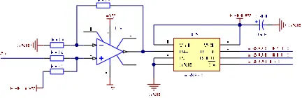
Railway frequency shift signal range from tens of mV to several hundred V range, span larger, in order to make the signal to meet the A / D sampling chip sampling range, AQW214 optocoupler relay and PGA103 gear gain control circuit to carry out gear shift and gain control. The specific circuit is shown in Figure 2.
The PGA103 is a general-purpose, programmable op amp that allows the FPGA to set the PGA103's magnification to 1, 10, or 100 by controlling both A0 and A1 inputs. The FPGA control PGA103, making the system gain magnification controllable, after the amplified signal into the A / D to do A / D conversion.
AD CONVERSION CIRCUIT
The system uses TI's successive approximation serial 16-bit micro-power high-speed A / D converter ADS8320. The maximum sampling frequency can reach 100kHz.
[image:3.612.190.406.282.352.2]This system adopts 3.3V to ADS8320 power supply, ADS8320 maximum input voltage range is 0-Vcc, the input signal can be input single ended or differential input in two ways, the system adopts the single end input mode, the -IN ground, reference voltage by Vcc, the frequency shift signal has a negative voltage to the signal accurately, need the voltage lifting circuit specifically, system uses the addition circuit lifting signal voltage, the voltage is Vcc/2. The schematic diagram of the voltage rise circuit of the A/D converter circuit is shown in Figure 3.
Figure 3. Schematic diagram of voltage rise circuit of A/D converter circuit.
FPGA CIRCUIT DESIGN
After the A / D conversion, the frequency-shifted signal is serially input to the FPGA, and the FPGA performs filtering analysis, calculation and processing, and displays the real-time data on the LCD screen. The whole FPGA belongs to the digital signal circuit part. In order to reduce the mutual interference between the front-end analog signal and the digital circuit, the system separates the analog circuit and the digital circuit to make the board and transmits the data and the control signal through the cable.
SYSTEM SOFTWARE DESIGN
Figure 4. Embedded software system structure.
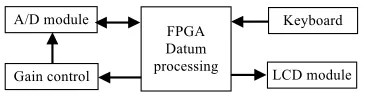
As shown above, FPGA control ADS8320 for A/D conversion of the signal, the signal data after A/D conversion into FPGA filtering analysis, analytical results show that in LCD, but also can be saved to the memory; at the same time FPGA according to the control signal gain test results, in order to meet the signal input range of A/D; in addition, the independent type although the keyboard connected to the FPGA pin, but FPGA is a key to determine the role of the judgment result is sent to the microcontroller, microcontroller according to the key instructions to control the whole system.
FPGA PROGRAM DESIGN
This system uses the Cyclone series FPGA EP3C40F484C8 of ALTERA company to design. The main task of FPGA including the A/D sampling, FIR digital filter and data processing and display, the program design is mainly done in the Quartus II environment, the system module structure diagram as shown in figure 5.
Figure 5. Structure diagram of system top level module.
VCC clk INPUT VCC AD7920_SDATA0 INPUT VCC AD7920_SDATA1 INPUT VCC reset_n INPUT VCC
KEY [11..0] INPUT
Inctrl_CH0[2..0] OUTPUT Inctrl_CH1[2..0] OUTPUT AD7920_SCLK0 OUTPUT AD7920_CS0 OUTPUT PGA0_A[1..0] OUTPUT PGA1_A[1..0] OUTPUT Key Out[3..0] OUTPUT Key Int OUTPUT AD7920_SCLK1 OUTPUT AD7920_CS1 OUTPUT V_Fs_Firo OUTPUT V_f rq_Firo OUTPUT
V_f s_f ir1
OUTPUT
V_f rq_f ir1
OUTPUT
V_f s_f ir2
OUTPUT
V_f rq_f ir2
OUTPUT
V_f s_f ir3
OUTPUT
V_f rq_f iq3
OUTPUT V_f s_Fir4 OUTPUT V_f rq_Fir4 OUTPUT V_FS_Fir5 OUTPUT V_Frq_Fir5 OUTPUT V_f rq_Fir6 OUTPUT V_FS_FIR7 OUTPUT V_Fs_Fir6 OUTPUT clk ADS8320_OUT ADS8320_CS ADS8320_CLK dataout[15..0] ADS8320 inst4 clk ADS8320_OUT ADS8320_CS ADS8320_CLK dataout[15..0] ADS8320 inst6
KEY _IN[11..0] KEY _OUT[3..0] IntOut Key _Prc inst15 clk datain[15..0] dataout[31..0] DC_Process inst12 clk datain[15..0] dataout[31..0] DC_Process inst13 clk reset_n current_Flag FSK0_FO[31..0] FSK0_Flow[31..0] FSK1_FO[31..0] FSK1_Flow[31..0] FSK2_FO[31..0] FSK2_Flow[31..0] FSK3_FO[31..0] FSK3_Flow[31..0] FSK_Curr0[31..0] FSK_Curr1[31..0] FSK_Curr2[31..0] FSK_Curr3[31..0] FSK_Curr4[31..0] FSK_Curr5[31..0] FSK_Volt0[31..0] FSK_Volt1[31..0] FSK_Volt2[31..0] FSK_Volt3[31..0] FSK_Volt4[31..0] FSK_Volt5[31..0] FSK_Volt6[31..0] Frq25_Volt_CH0[31..0] Frq25_Volt_CH1[31..0] Frq25_Phase[31..0] Frq25_Frq[31..0] ADCDataInCH0[15..0] ADCDataInCH1[15..0] AllValue_CH0[31..0] AllValue_CH1[31..0] Max_CH0[15..0] Min_CH0[15..0] Max_CH1[15..0] Min_CH1[15..0] FSK_Curr_DC[31..0] Mega_DataIn[7..0] Mega_Addr[7..0] Mega_RD Mega_WR InCtrl_CH0[2..0] InCtrl_CH1[2..0] PGA0_Gain[1..0] PGA1_Gain[1..0] Mega_DataOut[7..0] sy s_state[4..0] Zero0[15..0] Zero1[15..0] Sy stem_Process inst3 clk100M reset_n State_Sel[4..0] Data_In_CH0[15..0] Data_In_CH1[15..0] Current_Flag FSK0_F0[31..0] FSK0_Flow [31..0] FSK1_FO[31..0] FSK1_FLow [31..0] FSK2_FO[31..0] FSK2_Flow [31..0] FSK3_FO[31..0] FSK3_Flow [31..0] FSK_Curr0[31..0] FSK_Curr1[31..0] FSK_Curr2[31..0] FSK_Curr3[31..0] FSK_Curr4[31..0] FSK_Curr5[31..0] FSK_Volt0[31..0] FSK_Volt1[31..0] FSK_Volt2[31..0] FSK_Volt3[31..0] FSK_Volt4[31..0] FSK_Volt5[31..0] FSK_Volt6[31..0] AllvirtualValue0[31..0] AllvirtualValue1[31..0] Volt25_Ch0[31..0] Volt25_Ch1[31..0] Valid_FIR0 FS_FIR0 FRQ_FIR0 Valid_FIR1 FS_FIR1 FRQ_FIR1 Valid_FIR2 FS_FIR2 FRQ_FIR2 Valid_FIR3 FS_FIR3 FRQ_FIR3 Valid_FIR4 FS_FIR4 FRQ_FIR4 Valid_FIR5 FS_FIR5 FRQ_FIR5 Valid_FIR6 FS_FIR6 FRQ_FIR6 Valid_FIR7 FS_FIR7 Phase25[31..0] Frq25[31..0] Low 0_Out Low 1_Out Low 2_Out Low 3_Out clk_6K66 clk_66K6 Block_Signal_Process inst
Cy clone IV E inclk0 f requency : 25.000 MHz Operation Mode: Normal Clk Ratio Ph (dg) DC (%) c04/10.0050.00 c11/250.0050.00 c21/2500.0050.00 c38/1250.0050.00
[image:4.612.106.486.434.627.2]A/D Sampling Design
The A/D sampling chip used in this system is a 16 bit serial high speed A/D converter ADS8320.
According to the above timing, the system uses VHDL hardware description language to design A/D control module. Some of the procedures are as follows:
ARCHITECTURE arc OF ADS8320 IS
signal bitcnt,cnt: std_logic_vector(5 downto 0); signal temp: std_logic_vector(23 downto 0); begin
ads8320_CLK<=clk; process(clk)
begin
if clk'event and clk='0' then if cnt<22 then
ads8320_CS<='0'; else
ads8320_CS<='1'; end if;
end if; end process; process(clk) begin
if clk'event and clk='1' then if cnt<23 then
cnt<=cnt+1; else
cnt<=(others=>'0'); end if;
bitcnt<=bitcnt+1;
temp<=temp(22 downto 0) & ads8320_OUT;
if cnt=22 then
dataout<=temp(15 downto 0); end if;
end if; end process; end arc;
Fir Filter Design
different filter banks are designed to filter the signals with different frequencies. After the signal is filtered, the frequency and the effective value of the voltage are measured.
The FIR filter is realized by hardware FPGA, and the FIR filter is designed by using FIR Compiler in Quartus. Using FIR filter IP core design, has the advantages of less resources, short cycle, stable performance.
Due to the complexity of the frequency-shifted signal, to fully analyze it, multiple filter banks are needed to perform multiple filter processing. Using the filtered signal data for further analysis, the frequency offset value of the frequency-shifted signal low frequency value and RMS voltage are obtained. Specific design is as follows:
Open the Quartus II DSP Builder Toolbox, find the FIR Compiler design tool, and set the filter parameters. Taking the center frequency value and voltage value of 1700Hz as the example, a band pass filter with passb and of 1600Hz-1800Hz is designed. The window function type is blakman type and the order of filter is 500 steps. From the design window can see the frequency response of the design filter.
Voltage RMS Calculation Module
After the FIR filter frequency shift signal, enter the voltage measurement module for frequency measurement and voltage effective value reading, discrete
signal voltage effective value measurement formula is
2
1 1
( )
n
i f i
n , n is the sampling
point in unit time, f (i) is sampling signal instantaneous value.
FPGA program design of complex tasks, in addition to several main modules described above, there is a frequency measuring module, FPGA and MCU communication module, key detection module.
REFERENCES
1. Cui Lizhen, Du Puxuan. The investigation of technical solution based orthogonal frequency shift signal [J] microcomputer information, 2008 (21): 234-235.
2. Lin Yuyun, Li Peng, Li Daifeng, et al. Introduction to new railway signal technology [M]. China Railway Publishing House, 2005:126-129.
3. Li Kaicheng, Junjie Mao. A survey of new technologies of overseas railway communication signals [M]. China Railway Publishing House, 2005:1-22.