2016 International Conference on Electronic Information Technology and Intellectualization (ICEITI 2016) ISBN: 978-1-60595-364-9
Summarization of the Design and Control
Algorithm of the Multilevel Inverter
Risheng Lin, Hui Yu, Dafang Wang, Gang Liu and Xinyi Li
ABSTRACT
Multi-level inverter received great attention, because of its less harmonic content, low voltage stress and small switch loss. With the application of space vector pulse width modulation (SVPWM) control algorithm, the precision, responding time, security and stability of the pulse width gating signals can be improved conspicuously. In this article, we will make a conclusion about the normal topology and the control algorithm of the multi-level inverter.
INTRODUCTION
As the high power electronic equipment with the high pressure has been developing, the inverter has gradually turned to be the three-level or multi-level from the two-level[1-5]. The three-level inverter―one kind of relatively mature topological circuit about multi-level inverters, which owns such advantages as the big output capacity, the high output voltage and the small content of the current harmonics. In the field of the frequency control on the high pressure and high-power ac motor, the three-level inverter has been widely put into use[6-8]. In this article, we will make a conclusion about the normal topology and the control algorithm of the three-level inverter.
_______________________
Dafang Wang, Risheng Lin, Gang Liu, Xinyi Li, Harbin Institute of Technology, Weihai, Shandong, China, 264209
THETOPOLOGY OF THE MULTI-LEVEL INVERTER
The Topology of The I-type Three-level Diode Clamped Inverter
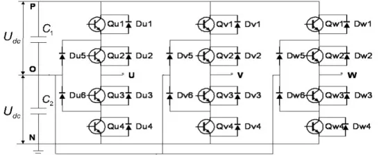
The concept of the multi-level neutral-point-clamped inverter was firstly presented in 1980 by a Japanese scholar named A. Nabae[9]. The topological structure is shown in the figure 1. In figure 1, the three-level inverter's power is supplied by two tandem power sources whose voltage are both Udc, thus the voltage
in the direct current side is double Udc. In the both sides of the DC power, there are
C1 and C2 as the two tandem capacitances, which play the role in bisecting the voltage of the DC power source. As a result, the voltage between the center point and the ground is Udc. Qxi(i=1~4, x=u,v,w) are same IGBT, Dxi(i=1~4, x=u,v,w)
are diodes anti-paralleled with IGBT.
The Topology of The T-type Three-level Diode Clamped Inverter
[image:2.612.161.434.398.510.2]Another normal topological structure of this kind of inverter is the T-type topology, which is shown in the figure 2.The difference between the T-type and the I-type is that the two switch Qx2 and Qx3(x=u, v, w) are connected in series between the center point O and the connection point of the switches Qx1 and Qx4 (x=u, v, w). In the working process of the T-type three-level inverter, when the output voltage is 2Udc, it just need to open the Qx1 (x=u, v, w); when the voltage is 0, it just need to open Qx4 (x=u, v, w).
Figure 1. The topology of the I-type three-level diode clamped inverter.
[image:2.612.132.463.552.662.2]Figure 3. Space voltage vector of three-level inverter. Figure 4. The diagram of small hexagon area.
THECONTROL ALGORITHMOF THE THREE-LEVEL INVERTER
We now have several kinds of control algorithms of the three-level inverter, which include SPWM[10], SHEPWM[11] and SVPWM. Among these algorithms, as the result of these characteristics such as the high voltage utilization ratio, the low harmonic content of output waveform, and the easiness in digital realization, the space vector module method(SVPWM) become the relatively popular control algorithm.
1 The Space Vector Partition
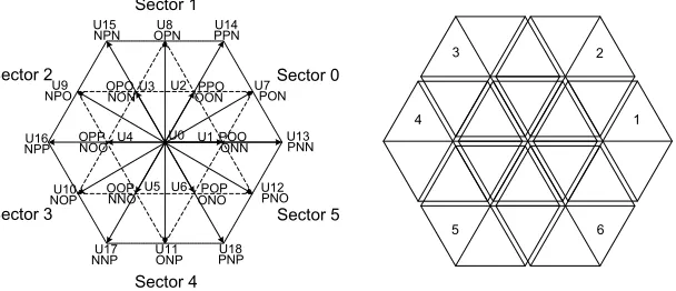
Each phase's bridge has P, O and N―three kinds of output condition. The condition P means the output voltage is 2Udc; the condition O means the output voltage is Udc; and the condition N means the output voltage is 0. As a result, the three-level inverter can compound 3*3*3=27 kinds of space voltage vector, among which there 19 kinds are useful. The label and spatial distribution of the space voltage vector are shown in the figure3.
According to the size of these vector norms, we can divide the space voltage vectors into 4 kinds: the zero vectors, the short vectors, the middle vectors, and the long vectors. U0(NNN,PPP,OOO) belongs to the zero vectors; U1(ONN,POO), U2(OON,PPO), U3(NON,OPO), U4(NOO,OPP), U5(NNO,OOP), U6(ONO,POP) belong to the short vectors; U7(PON), U8(OPN), U9(NPO), U10(NOP), U11(ONP), U12(PNO) belong to the middle vectors; U13(PNN), U14(PPN), U15(NPN), U16(NPP), U17(NNP), U18(PNP) belong to the long vectors. The big hexagon area made by these connected 6 vertices of the long vectors includes all the target vector vertex, in which these 6 long vectors have divided the area into 6 triangle sectors (Sector0-Sector5). PNN POO ONN U1 OOP NNOU5 U13 PON U7 PPNU14 OPNU8 NPN U15 NPOU9 NPPU16
NOPU10 PNOU12
PNPU18 NNPU17 ONPU11
PPO OON U2 POP ONO U6 OPO NONU3 OPP
NOO U4 U0
2 The SVPWM Algorithm of Three-level Inverter
The space vector diagram of the three-level inverter is composed with 6 small hexagons constituted by conventional two-level space vectors, and each small hexagon use the vertex of the internal small hexagon, showed in figure 4, as the center. The three-level voltage space vector plane uses U0 as the center, while if we want to simplify it as two-level, it is necessary to transfer the reference voltage space vector into the small hexagon, and use the small hexagon as the synthesis expectation to export the voltage space vector plane. Utilizing the formula (1) to convert the reference voltage vector.
iref ref i
U U U i1~6 (1)
As the case of i=1 shows, after the transformation, the reference voltage vector will be like the figure 5 showing. We can get formula (2).
1 1 1 1 2 1 2 0 1 0
s ref
T U t U t U t U (2)
In formula (2):U1ref = Uref-U1; 1 = U13-U1; 2 = U7-U1;0 = U1-U1; Ts is the PWM control period; t1 is vector U1-1 acting time; t2 is vector U1-2 acting time; t0 is vector U1-0 acting time.
Simultaneously adding TsU1 to the both sides of the formula (2), the simplified result is this:
1 13 2 7 0 1
s ref
T U t U t U t U (3)
[image:4.612.237.358.545.644.2]By the things above, we can get to know that the action time of the three-level space vector calculated by utilizing the two-level SVPWM is equivalent. As a result, when the reference voltage vector stands in other sectors, we can also convert the three-level SVPWM into two-level to calculate.
Figure. 5. The transformation of reference voltage vector.
U1 U13
U7
U12 U2
U6 U0
Uref
U1ref
U1-1 U1-2 U1-3
U1-4
CONCLUSIONS
This article has introduced several kinds of normal topology and control algorithm of the three-level inverter, analyzed characteristics of these structures, and also simply deduced the calculating process of the three-level inverter SVPWM. In general, compared to the conventional two-level inverter, the three-level inverter has the smaller harmonic content of the output waveform, the more similarities between the output waveform and the sine wave, and the better overall performance.
ACKNOWLEDGEMENTS
1.The National international scientific and technological cooperation projects of China(2014DFB70120)
2. The Science and Technology Development Plan Project of Weihai City(2014DXGJ02)
3. The Science and Technology Development Plan Project of Shandong Province(2014GGX105002)
4. The National Natural Science Foundation of China(51305457)
REFERENCES
1. J. Rodriguez, J.S. Lai and F.Z. Peng. 2002. “Multilevel inverters: a survey of topologies, controls, and applications” IEEE Trans. On Industrial Electronics, 49(4): 724-738
2. Brendan Peter McGrath, Donald Grahame Holmes, Thomas Lipo, et all. 2003 “Optimized space vector switching sequences for multilevel inverter” IEEE Trans. Power Electron, 18(6):
1293-1301.
3. D. Grahame Holmes, Thomas A. Lipo. 2003. Pulse Width Modulation for Power Converters.
New York: John Wiley & Sons Inc.
4. Jose Rodriguez, Steffen Bernet, Bin Wu, et all. 2007. “Multilevel voltage-source-converter topologies for industrial medium-voltage drives” IEEE Trans. On Power Electronics, 1(54):
2930-2945.
5. Franquelo, L.G. Rodriguez, J. Leon, et al.2008. “The age of multilevel converters arrives”
Industrial Electronics Magazine, IEEE, vol. 2, 28-39.
6. Weidong Jiang, Qunjing Wang, Quan Chen. 2008. “SVPWM algorithm for NPC three-level VSI considering unbalance neutral point voltage” Proceedings of the CSEE, 28(30): 20-26. (In
Chinese)
7. Xiangning He, Yansong Wu, Bingjian Yang. 2012. “Real-time state monitoring during switching model transitions in high power three-level inverters” Proceedings of the CSEE, 32(30): 54-60.
(In Chinese)
8. Pou J., Pindado R., Boroyevich D., et al. 2005. “Evaluation of the low frequency neutral-point voltage oscillation in three-level inverter” IEEE Transactions on Industry Applications, 52(6):
1582-1588.
9. Nabea A., Takahashi I., Akag H.I. 1981. “A new neutral-point-clamped PWM inverter” IEEE Transactions on Industry Applications, IA-17(5): 518-523.
10. Jian Liu, Xiang-gen Yin, Zhe Zhang, et all. 2008. “Study of SPWM Digital Technologies for High-voltage High-power Three-level NPC Inverter” Proceedings of the CSEE, 28(27): 35-41.