Design of Topologies of Current Controlled Current
Conveyor in 16 nm Bulk CMOS Technology
Mohd.Faseehuddin
1, Sadia Shireen
2
1, 2 M.Tech Student, EC department, Integral University, Lucknow, Uttar Pradesh, India
Abstract- Advancement in VLSI technology has led to larger number of components on a single chip making it a reality to realise portable systems. Analog circuits are important in every VLSI systems such as filters, current and voltage amplifiers, comparators, A/D and D/A converters, etc. Miniaturization in circuit design requires low-power low-voltage (LPLV) analog integrated circuits to be designed. Analog signal processing’s inherent advantage of low power and high speed has led to extensive research in analog domain. Current domain processing having advantages of higher bandwidth, large dynamic range, greater linearity, simple circuitry seems to be the solution. Among the number of current mode topologies current conveyor is the most versatile building block. The second generation Current controlled current conveyor (CCCII) has attained greater popularity in recent years due to electronic adjustability of its X-terminal intrinsic resistance through bias current. Here we have designed three topologies of CCCII found in literature namely dual output current controlled current conveyor (DOCCCII), current controlled current conveyor transconductance amplifier (CCCCTA) and digitally programmable current controlled current conveyor (DPCCCII) in 16nm bulk CMOS technology using PTM (High Performance 16nm Metal Gate / High-K / Strained-Si parameter).
Index Terms- Current Conveyor, DOCCCII, CCCCTA, DPCCCII
I. INTRODUCTION
With scaling down of CMOS to comply with large scale integration and system on chip requirements together with increased demand for portable and battery operated devices, low power low voltage (LP LV) devices are need of the hour. The current mode devices are more suited for (LP LV) operation than their voltage counterpart [1, 2]. Current mode circuits are more immune to noise, less sensitive to supply voltage and have low electrostatic discharge, low propagation delay, high slew rate etc. [2,4]. Among various current mode devices current conveyor (CC) is the most functional device by virtue of its versatile features such as simplicity in design, higher gain bandwidth product, linearity, high frequency operation, less chip area, low power dissipation [4-7] etc. In 1968 [1] the current conveyor (CC) was introduced and has since found recognition in both conceptual and practical implementation. Researches published in last few years reveals that analog circuit designers are now considering the CC as a building block for designing multitude of applications like signal processing, amplification, instrumentation etc. [1,8,9]. A CC is a three terminal device having a low impedance input, a high impedance input simultaneously with a characteristic of virtual short and a high
current controlled current conveyor (CCCII) gathers larger attention from designers due to its high tunability [1,2,10]. CCCII has in built parasitic resistance which is self-adjustable by bias current, due to this parasitic resistance the requirement of external resistance is reduced. Practical CC has various non-idealities and some of them prove their importance in different applications [11, 12]. Parasitic resistance of CCCII is one of its useful non idealities. Literature shows there are many tunable circuits i.e. current differencing transconductance amplifier (CDTA) [13], current follower transconductance amplifier (CFTA) [14,15], current controlled current conveyor transconductance amplifier (CCCCTA) [16-18], digitally programmable current conveyor (DPCCII) [19,20] etc. In this work we will be designing CCCCTA, DPCCCII and DOCCCII among various topologies of CCCII in 16 nm bulk CMOS and discuss their features.
II. CCCII AND ITS TOPOLOGIES
After its introduction in 1995 [10] CCCII has been the first choice of analog designers mainly because it includes a X- node parasitic resistance which can be electronically controlled through the input bias current and so needs no additional resistance for activation. Current negation and current duplication is very easy to obtain in case of a CCCII, leading to DOCCCII. The equivalent circuit symbol and the principal equation of DOCCCII are given in FIG.1 and Eq.1. DOCCCII has two high impedance current output nodes which provide quadrature signals.
FIG.1.BLOCKDIAGRAMOFDOCCCII
[
]
=
[
] [
]
(1)
=
IY IB DOCCCII X Y Z+ Z-
IX IZ+
Where is the parasitic internal resistance at port X and is controlled by bias current .
The CMOS implementation of a class AB DOCCCII is presented in FIG. 2. The circuit consists of a translinear loop consisting of transistors M1 – M4. Two MOS current mirrors ( M5 – M6 and M7 – M8) are used to bias the translinear loop with bias current , The input cell presents a high input impedance at input port Y and a low input impedance at input port X. This cell acts as voltage follower. The current at node X is copied to the output nodes Z+ and Z–. Currents Id18 and Id14 are cross-coupled
through transistors M14, M15, M18 and M19 to generate negative current at Z- node. Details are shown in the circuit given in FIG. 2.
FIG.2.DUALOUTPUTCURRENTCONTROLLEDCONVEYOR
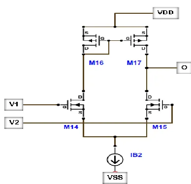
A. CCCCTA AND ITS DESCRIPTION
It is a four terminal device whose input stage is a CCCII and output stage is made of an operational Transconductance amplifier. The core of the circuit is the differential pair with active load which is used to achieve tunable Transconductance and hence a tunable current gain. The output current of the CCCII is converted in to voltage due to the lumped parasitic capacitances of CCCII and the differential pair. The transistors M14 and M15 function as a differential amplifier to convert the input voltage to an output current. The transistors M16 and M17 acts as a current mirror with IB2 as input bias current as shown in FIG. 3 When is applied it establishes I14 and I15 in M14 and M15 respectively. The relation between and output current Io is given in Eq.2.
I
o= − (2) Where transconductance ratiosIf = =
I
o=-
) (3)
Where=
√
(4)
From Eq. 3 & 4 [17] it can be deduced that the input current can be tuned by varying the bias current of transconductance amplifier IB2.
The equivalent circuit symbol, port relationship and CMOS implementation of CCCCTA are given in FIG.4, Eq. 5 and FIG.5 respectively.
[
]=[
] [
] (5)
It can be used in both current mode and voltage mode circuits including hybrid (voltage-current) circuits. Authors of [16-18] have demonstrated its versatility by realizing current mode filters, oscillators, inductor etc.
FIG.4.BLOCKDIAGRAMOFCCCCTA FIG.3.TRANSCONDUCTANCEAMPLIFIER
IY
IB1
CCCCTA X
Y
O Z
IX ±Io
[image:2.612.355.549.61.248.2] [image:2.612.39.277.240.439.2] [image:2.612.326.540.573.650.2]FIG.5.CURRENTCONTROLLEDCURRENTCONVEYORTRANSCONDUCTANCEAMPLIFIER
B. DPCCCII AND ITS DESCRIPTION
Recently many researches have reported digitally controlled CC [19, 20], the introduction of digital control to CC has increased its functional capability and versatility and eased the on chip control of devices with high resolution capability and reconfigurability [19].
Researchers have used numerous techniques to incorporate digital control in to CC. In this work we have used a current summing network (CSN) as the output stage to get digital control over the current gain, the input stage being the CCCII .CSN mainly consists of array of NMOS & PMOS transistors and their associated switches as shown in FIG.6.The switches (M14a-M19a) in the CSN are controlled by digital code word. A particular branch of the CSN can be activated or deactivated by applying the appropriate code word. The current flowing out of the CSN is the sum of the currents from the activated branches, giving a current gain of ‘K’, and is given by Eq.7. The block representation of DPCCCII is given in FIG.7.
The aspect ratios of CSN transistors are given by:
( )
= ( ) ( ) = ( ) i ={ } (6)
The current if flowing out of Z terminal can be expressed by:
=∑ (7) FIG.6DIGITALLYPROGRAMMABLECURRENTCONTROLLED
CURRENTCONVEYOR
FIG.7BLOCKDIAGRAMOFDPCCCII
IY
IB
DPCCCII X
Y
Z IX
IZ
Current gain provided by DPCCCII equal to:
=∑ (8) Term represents the digital control word applied to the branch in CSN. It enables or disables a particular branch of CSN.
III. SIMULATION RESULTS
The topologies of CCCII namely DOCCCII, CCCCTA and DPCCCII are simulated in H-spice using 16nm bulk CMOS PTM [21] to point out the advantage of each. A detailed comparison of the simulation results of the various topologies are given below.
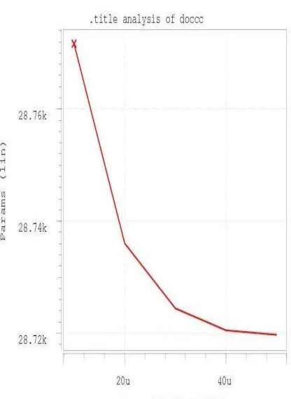
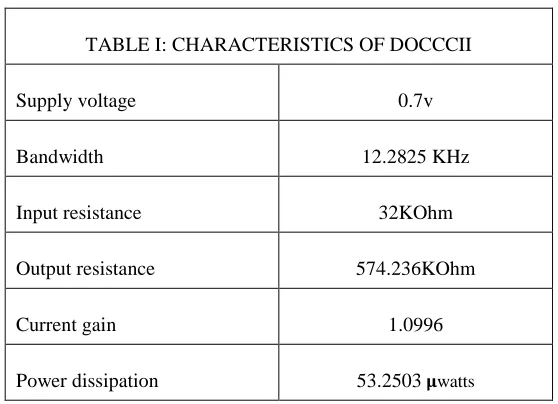
FIG. 8 & 9 shows the AC and transient analysis of DOCCCII. AC analysis gives the range of frequencies of operation. Transient analysis has been carried out with 1 GHz frequency for sinusoidal input undistorted output. At frequencies higher than 2 GHz there is a phase shift in the output so its actual range of frequency is 1Ghz.The simulation results are summarized in the TABLE I given below.
FIG.8TRANSIENTANALYSISOFDOCCCII
In FIG. 10 RX vs. bias current variation of DOCCCII is shown.
FIG.9 ACANALYSISOFDOCCCII
[image:4.612.336.531.70.300.2] [image:4.612.335.548.72.618.2] [image:4.612.344.552.329.614.2] [image:4.612.72.265.362.592.2]FIG.11 TEMPSTABILITYOFDOCCCII
[image:5.612.73.269.68.327.2]In FIG. 11 temp stability of DOCCCII is shown.
TABLE I: CHARACTERISTICS OF DOCCCII
Supply voltage 0.7v
Bandwidth 12.2825 KHz
Input resistance 32KOhm
Output resistance 574.236KOhm
Current gain 1.0996
Power dissipation 53.2503 𝛍watts
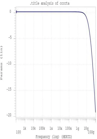
The AC response of CCCCTA is plotted with different values of IB2 and the obtained response is given in FIG. 12, 13, 14 and 15. The simulation results are summarized in TABLE II. In FIG.12 ac analysis of CCCCTA is given and in FIG.13 current gain
between Ioand IX in dB is given against frequency.
FIG.12ACANALYSISOFCCCCTA
[image:5.612.313.542.102.409.2] [image:5.612.28.307.415.617.2] [image:5.612.340.525.457.643.2]FIG .14 CURRENT GAIN OF IZ AND IX OF CCCCTA
[image:6.612.59.254.82.360.2]In FIG .14 the current gain between IZand IX in dB and in FIG .15 variation of RXagainst bias current is given.
TABLE II: CHARACTERISTICS OF CCCCTA
Supply voltage 0.7V
Bandwidth 3.33 GHZ
Output Resistance 231 KΩ
Power dissipation 182.2810µwatts
FIG.16ACANALYSISOFDPCCCII
FIG.16 shows ac response of DPCCCII, in this response different gain values are obtained when different branches are ON.
TABLE III: CHARACTERISTICS OF DPCCCII
Supply voltage 0.7v
Bandwidth 2.0314GHz
Output resistance 144.210KOhm
Input resistance 27KOhm
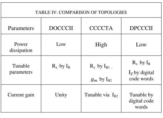
[image:6.612.326.575.171.492.2] [image:6.612.66.268.478.718.2]TABLE IV: COMPARISON OF TOPOLOGIES
Parameters DOCCCII CCCCTA DPCCCII
Power dissipation
Low High Low
Tunable parameters
Rx by IB Rx by IB1 , by IB2
Rx by IB IZ by digital code words
Current gain Unity Tunable via IB2 Tunable by
digital code words
IV. CONCLUSION
The 3 topologies of CCCII are simulated and studied in 16 nm technology to point out the importance of each. The flexibility of programming of different topologies can be used to synthesize variable gain filters and oscillators with tunable frequency, voltage and current amplifiers of varying gain. These topologies can be used as a building block for field programmable analog array (FPAA).
REFRENCES
1. S. Sedra, et al., “The Current Conveyor: History, Progress and New
Results,” IEE Proceedings (Part G) of Circuits, Devices and Systems, Vol. 137, No. 2, April 1990, pp. 78-87. doi:10.1049/ip-g-2.1990.0015
2. Giuseppe Ferri and Nicola .C.Guerrinni, “Low voltage low power CMOS current conveyors”, Print ©2003 Kluwer academic publishers, Dordrecht.
3. Giuseppe Palnisano, Gaetano Palumo, Salvatore Pennisi, “CMOS Current Amplifiers”, Kluwer Academic publishers, 1999.
4. F. Yuan, “CMOS Current-Mode Circuits for DATA Communications”, Springer Verlag, 2007.
5. C.H. Lee, J. Cornish, K. McClellan, J. Choma Jr., “Current-Mode Approach for Wide-Gain Bandwidth Product Architecture”, IEEE Trans. Cir. Sys. II, Vol. 45, May 1998.
6. L.N. Alves, R.L. Aguiar, “A Differential Current-Conveyor Based Buffer for High-Bandwidth Low-Signal Applications”, ICECS99, Paphos, Cyprus, Sep.
7. B. Wilson, “Recent developments in current conveyors and current mode circuits,” IEE Proceedings-G, pp. 63 – 77, 1990
8. R. Senani, “Novel circuit implementation of current conveyors using an OA and an OTA,” Electron. Lett. , vol. 16, no. 1, pp. 2–3, Jan. 1980.
9. B. Wilson, “Recent developments in current conveyors and current mode circuits,” IEE Processing, Pt. G, vol. 137, pp. 63-77, April, 1990.
10. A.Fabre, O. Saaid, F. Wiest, and C. Baucheron, High frequency applications based on a new current controlled conveyor, IEEE Transactions. Circuits System-I, vol. 43,no. 2, pp. 82-90,
11. M.Y.Yasin, Bal Gopal “High Frequency Oscillator Design Using a Single 45 nm CMOS Current Controlled Current Conveyor (CCCII+) with Minimum Passive Components” Circuits and
12. Pipat Prommee,Montri sondunyakanok, “ CMOS based current controlled DDCC and its applications to capacitance multiplier and universal filter” Int.J.Commun.(AEU) 65 pp.1-8, 2011.
13. A. U. Keskin, D. Biolek, E. Hancioglu and V. Biolkova, Current-mode KHN filter employing current differencing transconductance amplifiers, Int’l J. Electronics and Comm. 60 (2006) 443-446 14. N. Herencsar, J. Koton and K. Vrva, Single CCTA-based universal
biquad filters employing minimum components, Int’l J. Computer and Electrical Eng. 1307-310¸(2009).
15. T. Thosdeekoraphat, S. Summart, C. Saetiaw, S.Sanatalunai and C. Thongsopa, Resistor-less current mode universal biquad filter using CCTAs and grounded capacitors, World Academy Of Science, Eng. and Tec. 69 ,559-563, (2012).
16. S. V. Singh, S. Maheshwari and D. S. Chauhan, Universal current-controlled current-mode biquad filter employing MO-CCCCTAs and grounded capacitors, J.Circuits and Syst.1, pp.35-40. 2010
17. Winai jaikala, Montree Siripruchyanum, Phamorn Silapan, “ Realization of CMOS Current Controlled Current Conveyor Transconductance Amplifier CCCCTA and Its Applications” J. of Active and Passive Electronics Devices,Vol.4,pp.35-40,2009. 18. Sajai Vir Singh,Sudhanshu Maheshwari “Processing
Current-Controlled, Universal Biquad Filter”,Radio Engineering,Vol.21,no1, April 2012
19. Iqbal.A.Khan,Ahmed.M.Nahhas, “Current Mode Programmable Analog Modules using Low voltage .Digitally Controlled CMOS CCII”, International Journal Of Computer applications(0975-888),vol.48,no4,June 2012
20. T.M.Hassan, S.A.Mahmoud,“New CMOS Digitally Controlled Variable Gain Aplifier” International Conference On Microelectronics, 2008.
21. Predictive Technology Model, 2006 http://ptm.asu.edu. AUTHORS
First author- Mohd.Faseehuddin, pursuing M.Tech from Integral University, Lucknow.
Email id: [email protected]
Second Author- Sadia Shireen, pursuing M.Tech from Integral University, Lucknow.
Email id: [email protected]
Correspondence Author- Mohd.Faseehuddin Email id: [email protected]