N A N O E X P R E S S
Open Access
Non-equidistant scanning approach for
millimetre-sized SPM measurements
Petr Klapetek
1*, Miroslav Valtr
1and Petr Bur
š
ík
2Abstract
Long-range scanning probe microscope (SPM) measurements are usually extremely time consuming as many data need to be collected, and the microscope probe speed is limited. In this article, we present an adaptive
measurement method for a large-area SPM. In contrast to the typically used line by line scanning with constant pixel spacing, we use an algorithm based on several levels of local refinement in order to minimize the amount of information that would be useless in the data processing phase. The data obtained from the measurement are in general formed byxyzdata sets that are triangulated back with a desired local resolution. This enables storing more relevant information from a single measurement as the data are interpolated and regularized in the data processing phase instead of during the measurement. In this article, we also discuss the influence of thermal drifts on the measured data and compare the presented algorithm to the standard matrix-based measuring approach.
Background
Many novel industrial components, e. g. optoelectronic devices, microchips, diffraction gratings or photonic crys-tals, are typically formed by highly integrated microstruc-tures arranged on very large areas. The inspection and control of such components are problematic as we need to detect small imperfections on large areas or to evalu-ate small differences between many semiconductor mask critical dimensions. Scanning probe microscopy techni-ques (e. g. atomic force microscopy) can be used for this task if sufficiently large areas can be scanned. The bottle-neck of using scanning probe microscopes was always the scanning range; however today, specialized equip-ment can be found in the literature and even on the mar-ket [1-5] featuring very small uncertainties (less than 1 nm) over very large volumes. However, even if the range of microscopes has changed, the maximum speed of the tip is still nearly the same. Large-scale measure-ments are therefore very slow.
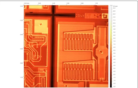
Even if we measure on very large areas, like those shown on Figure 1 for a microchip surface, only a very small part of the measured data isfinally used for the evaluation. From Figure 1, we would probably measure several critical dimensions on observed interconnections only. The rest of the data would be left aside even if it
took several hours to acquire them and even if they occupy hundreds of megabytes of disk space. This is a large waste of effort. One of the possibilities how to over-come this is to measure data in a non-equidistant approach (not creating a regular matrix of points during measurements). If we are able to measure the overall sample geometry with low resolution and local features that will be used for surface properties evaluation with high resolution, we can both speed up the measurement and reduce the need for data storage.
In this article, we discuss one possible realization of a non-equidistant measurement method for a long-range scanning probe microscope and discuss its applications for different samples typical for microelectronics and solar cell industry.
Methods
Experimental arrangement
A home-built long-range scanning system was used for the implementation and testing of the adaptive scanning algorithm [6]. It is based on commercial crossed-roller bearing stages combined with piezoceramic actuators used to compensate the imperfections of the bearing mechanism. Three interferometers are used for all three-axis translation monitoring and feedback. For stage rotation monitoring (axis normal to sample sur-face), an autocollimator is used. For non-planarity com-pensation and two more axis rotation comcom-pensations
* Correspondence: [email protected]
1Czech Metrology Institute, Okružní 31, Brno, 638 00, Czech Republic
Full list of author information is available at the end of the article Klapeteket al.Nanoscale Research Letters2012,7:213 http://www.nanoscalereslett.com/content/7/1/213
(axes parallel to sample surface), an optical quality refer-ence plane and a set of tunneling current sensors are used. The atomic force microscope head was used for determining the probe-sample distance and performing the z-axis motion (based on piezoceramic actuators). The construction of the system is illustrated in Figure 2 and in more detail described in [6]. The thermal stability of the system is assured using an active stabilization box with digitally controlled, thermally stabilized water.
[image:2.595.59.539.87.393.2]For illustrative measurements, three different samples were used: a calibration grating that is usually used for commercial scanning probe microscopes calibration, a microchip surface and a solar cell surface with a typical pyramidal structure used for light trapping. These repre-sent typical measurands requesting large-scale measure-ments combined with high-resolution details. Contact mode measurements were performed using standard contact tips from Nanosensors (PPP-CONTR series, Figure 1Large-area AFM measurement. Typical large-area measurement of the microchip surface using the atomic force microscope technique. The lateral dimensions inxandyaxes are approximately 1, 187μm.
Figure 2Long-range SPM schematics.(A)xyMotion system (position of three reference plane sensors and actuators shown as well) and(B)
[image:2.595.62.540.563.691.2]NANOSENSORS, Rue Jaquet-Droz 1, Case Postale 216, CH-2002 Neuchatel, Switzerland).
Adaptive measurement algorithm
There are numerous ways how to perform measurements of a rectangular surface area. Logically, the most straight-forward and mostly used approach is to measure in a rec-tangular grid mapping pixel to pixel and directly creating the image. Even if this is the most convenient scanning approach and the data can be processed very easily after measurement, it leads to a large loss of data already dur-ing the scanndur-ing process. As the microscope needs to maintain the feedback loop during the motion of the tip, the amount of the collected data in a single profile is usually much larger than the number of pixels of the resulting image (e. g. by an order or more). Data are then resampled to the requested number of pixels, loosing the high-resolution information already acquired in between them. A natural improvement of‘standard’square scan-ning probe microscope (SPM) image would therefore be a square set of data with non-rectangular pixel size, where fast axis spacing would be much smaller than the one of the slow axis. Implementing such a scanning method could already dramatically improve the amount of information collected in a single scan (in the same time), even if the method is still quite a regular one.
On the other side, adaptive sampling could be realized as forming a completely random distribution of points in thexyplane. Based on some surface properties, like local roughness, we could measure the data forming a comple-tely irregular set of points that would be triangulated afterwards. However, as the microscope in principle mea-sures high-resolution data over some continuous path, this could be ineffective. It is therefore desirable to mea-sure a set of profiles (not necessarily forming a Cartesian grid).
In order to simplify the problem, we started imple-menting a scanning algorithm based on acquiring rows and columns of different length, not organized in a regu-larly spaced matrix. The prerequisite of the presented iterative process is to decide what should be thefinalxy axes desired resolution and what is thez-axis precision we want to reach. The key points of the refinement algo-rithm are as follows:
1. Measure a net formed by rows and columns with coarsexyresolution and interpolate data to thefinal resolution.
2. Measure and add an interleaved net of rows and col-umns to form a data with resolution which is twice as
fine and interpolate data to thefinal resolution. 3. Identify subsets between rows and columns where the interpolated data between the last two iterations differ more than by a requestedzprecision criterion.
4. Where thezprecision criterion failed, measure a net of rows and columns with twice asfine resolution on those rectangles. Note that in order to save the mea-surement time, this process needs to be optimized so that the movement between different refinement areas is minimized. An optimum path for the SPM probe is therefore planned merging all the necessary move-ments (including movemove-ments between different areas) with the criterion of the shortest total distance. This is in principle a traveling salesman problem, and here, it is solved using the nearest neighbor algorithm.
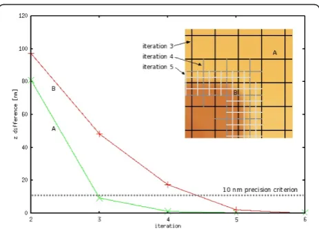
The whole refinement process is illustrated in Figure 3. If the surface exhibits regular areas (e. g. a microchip
sur-face), areas measured in each refinement iteration
[image:3.595.306.538.496.664.2]become smaller and smaller, up to a point where all data are measured with the requested z precision. In Figure 4, measured areas are shown for a calibration grating, a microchip surface and a solar cell light-trapping surface. Areas where thezprecision criterion failed are marked by black for the three levels of refinement. In these areas, a refinement in next iteration is planned and performed. It should be noted that for a completely random surface (white noise), thefinal number of data measured is twice larger than for a standard matrix measurement (we mea-sure both rows and columns independently). However, as the surfaces are typically locally continuous, we usually need to measure a much smaller number of data points than for a standard matrix measurement. Moreover, the suggested algorithm could in principle lead to missing a small structure in case that it would be missed in thefirst two iterations. The only solution to overcome this is not to use too coarse initial grid spacing.
Figure 3Adaptive measurement process illustration. The graph shows the convergence of thezvalue of a typical point on aflat sample area (point A) and close to a steep slope (point B) if the iterative refinement process is not stopped by the precision criterion. The precision criterion is used to stop refinements locally as shown in the inset.
Klapeteket al.Nanoscale Research Letters2012,7:213 http://www.nanoscalereslett.com/content/7/1/213
When we have the data measured, we cannot save them as a regular matrix, so we use a general set ofxyz values for storing the data. Algorithms available for SPM data processing however expect a regular matrix in most of the cases, and so do also the vast majority of software packages available for SPM data processing and analysis. The easiest way on how to overcome this is to regularize the data back before analysis - now with the desired resolution that can be locally much larger than for the coarse image. We can therefore perform zooms in the measured data - and where the data are densely sampled, we can obtain high-resolution details. For interpolation purposes, data are triangulated by a fast divide and conquer routine (similar to the one described in [7]) reaching optimal worst-case complexity of O(n logn), where n is the number of data used for triangula-tion. Recursive divisions alternate between horizontal
and vertical cuts. A Delaunay triangulation and a Voro-noi diagram are created using this approach. With Delaunay triangulation and Voronoi diagram computed, we can use a number of interpolation methods. At the moment, a simple planar interpolation of the triangu-lated data is utilized.
The presented algorithm was implemented using libraries of Gwyddion open source software for SPM data analysis http://gwyddion.net. While the scanning routines can hardly be shared to the public (these are connected to the microscope hardware), we expect that the tested triangulation and regularization approach will be made available to Gwyddion users as part of our future work.
Results and discussion
[image:4.595.56.540.88.471.2]1. It can save the amount of necessary measured information while measuring with very high resolu-tion, thus shortening the measurement time and minimizing the probe wear while preserving the necessary resolution on critical surface structures. 2. It allows the user to perform further local refi ne-ments easily while the sample is still in the micro-scope, not necessarily based on the algorithm criteria but also on the user’s requirements.
3. It can automatically measure the data allowing the user to perform zoomsoffline, e. g. in the data proces-sing phase after the measurement. This can be useful namely for automated image processing or inspection purposes.
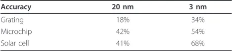
In order to document the effect of the reduction of the necessary scanned path, we compare the path length saved by the presented algorithm to the standard matrix-based approach for the surface shown in Figure 3. The resulting total tip path reductions for two differentfinal accuracies are summarized in Table 1. It can be noted that the more refinement levels are performed the more data are saved. This is however not valid generally but only on regular structures like the one presented here. As stated above, for completely random data, we cannot save anything using the refinement algorithm.
In order to display the real performance of the algo-rithm if implemented in the microscope, we compare the results of the matrix algorithm and the presented algo-rithm on real data of a calibration grating. The samefinal resolution was requested. In Figure 5, we can see the result of the subtraction of images obtained using the two algorithms. We can see that the local differences are caused only by relatively high noise of the presently used long-range system z scanner and a slight mismatch between the two images (due to a slight shift caused by retraction and approach between the two measurements, the images had to be cropped and aligned manually).
It should be noted that the obtained data have different statistical properties than a typical matrix-based SPM image. There is no difference between the fast and slow axes as bothxandydirections are used for the measure-ment. It has no sense therefore to distinguish between directions while evaluating direct or statistical quantities. All parasitic effects, such as drift or noise, influence data
almost isotropically. This could be understood as a draw-back in some sense; on the other side, it can simplify the treatment of uncertainties while obtaining profiles of dif-ferent orientation with respect to the main axes or 2D statistical properties evaluation.
An important issue is the influence of drift on the mea-surement process. Drift, namely of thermal origin, can be observed in many SPM systems [8,9]. In a typical matrix-based SPM image, drift is mainly seen in the slow scan-ning axis, leading to image distortion as seen in Figure 6B. Note that the coordinate system origin in this simulation is in the top left corner of the image. Based on the analysis of the known surface structures or based on repetitive scans, we can determine the drift rate, which is usually a time-dependent decaying function, with a maximum right after the instrument start-up or a sample exchange [10]. If we use the scanning approach presented in this work, the data in the image are not measured successively, so the straightforward drift determination from AFM image is not possible as the drift influences interleaved values sign-ificantly (see Figure 6C). However, drift can still be evalu-ated. As in each refinement level, we measure on the same area as was already measured in the previous iteration, and we even obtain data at exactly the same points (at row/column crossings); we can determine the drift rate already during refinement process for areas that are being refined. We can do this using the following approach:
•Create an interpolated image from one refinement level (using the standard procedure from the pre-vious section);
[image:5.595.305.539.89.219.2]•Create an interpolated image from the next level skipping the data measured in the previous level; Table 1 Performance of the measurement algorithm
Accuracy 20 nm 3 nm
Grating 18% 34%
Microchip 42% 54%
Solar cell 41% 68%
[image:5.595.56.291.653.705.2]This table summarizes the total tip path reduction for two differentfinal accuracies (20 and 3 nm). Note that 100% corresponds to the path needed for obtaining the regularly sampled data with the same accuracy.
Figure 5 Comparison of the matrix algorithm and the presented algorithm. Thisfigure shows the result of a subtraction of images obtained using the two algorithms. Note that the local differences are caused only by relatively high noise of present long-range systemzscanner and slight mismatch between the two images (due to a slight shift caused by retract and approach between the two measurements, the images had to be cropped and aligned manually).
Klapeteket al.Nanoscale Research Letters2012,7:213 http://www.nanoscalereslett.com/content/7/1/213
• Use cross-correlation to determine the shift between the two data sets (in all three axes), which are thexandy drift values; and
•Shift one data set according to the cross-correlation result and subtract the two data sets, which gives us thezdrift value.
As an illustration of the process, we have simulated data measurement with a constant drift vector of (3, 3, 0.3) nanometres per second in Figure 6. We have used the part of the microchip surface seen in Figure 6A, using already measured data (without observable drift) and adding the drift during the simulated measurement (all movements were performed with the same velocity). Drift was evalu-ated from levels 1 and 2 of the refinement process where, for this sample, we still measure on nearly the whole area (the local refinement criterion still holds everywhere). Using the above-mentioned process, we have evaluated the drift vector as (3.3 ± 0.5, 2.7 ± 0.3, 0.29 ± 0.15) nano-metres per second which is a good estimate of the drift
[image:6.595.60.541.345.691.2]rate. In Figure 6D, a simulated measurement with correc-tion based on this estimated drift rate is shown (for drift estimation, thefirst two iterations were used), obviously leading to significant correction of the image. Of course, if the drift rate is not constant, the above-mentioned approach would not be an optimal one; however, the user could repeat it after several refinement iterations to cor-rect the drift rate estimate. Generally, it can be seen that the drift leads to a much more evident image distortion when our adaptive refinement algorithm is used. On the other side, even the data obtained in a regular matrix approach are influenced by the drift, and if we do not know the measured structure properties, we need to use a similar correlation technique to determine the drift. Data are therefore‘wrong’ in both cases, but in the regular matrix case, they look better and allow the user to ignore the systematic errors caused by the drift. The large infl u-ence of the drift on the presented algorithm could there-fore be seen even as a benefit for a metrologist - if the systematic error is quantitatively the same in both cases
anyway, the adaptive approach prevents the fact that it would rest hidden in the data.
Conclusion
We have implemented an adaptive refinement
measur-ing algorithm in a long-range scannmeasur-ing probe micro-scope. For surfaces with large regular areas, the use of this adaptive scanning instead of a regular matrix scan-ning can save the time necessary for the measurement and enable high-resolution zooming in the measured data. This can be interesting namely when measuring large areas of different manufactured nano-and micro-structures, like electronic parts, photonic crystals, diff r-action gratings, etc. Using the presented approach, we iteratively measure with higher and higher resolution on critical surface areas, determined by a simple and uni-versal criterion. In the data processing phase, the set of
xyzdata obtained from the measurement is triangulated, and necessary details are regularized in order to reach requested resolution. This enables the user to perform zooming in the data processing phase, with no need of performing further measurements.
Acknowledgements
This work was supported by the Ministry of Trade and Commerce under contract number FR-TI1/241.
Author details
1Czech Metrology Institute, Okružní 31, Brno, 638 00, Czech Republic2Faculty
of Informatics, Masaryk University, Botanická 68a, Brno, 602 00, Czech Republic
Authors’contributions
PK carried out the development of the adaptive measurement algorithm. MV performed atomic force microscopy measurements on long-range SPM, and PB wrote software routines for generalxyzdata triangulation. All authors read and approved thefinal manuscript.
Competing interests
The authors declare that they have no competing interests.
Received: 30 September 2011 Accepted: 11 April 2012 Published: 11 April 2012
References
1. Werner C, Rosielle PCJN, Steinbuch M:Design of a long stroke translation stage for AFM.International Journal of Machine Tools & Manufacture2010, 50:183-190.
2. Manske E, Hausotte T, Mastylo R, Machleidt T, Franke KH, Jäger G:New applications of the nanopositioning and nanomeasuring machine by using advanced tactile and non-tactile probes.Meas Sci Technol2007, 18(2):520.
3. Eves BJ:Design of a large measurement-volume metrological atomic force microscope (AFM).Meas Sci Technol2009,20(8):084003. 4. Dai G, Pohlenz F, Danzebrink HU, Xu M, Hasche K, Wilkening G:
Metrological large range scanning probe microscope.Rev Sci Instruments 2004,75(4):962-969.
5. Sturwald S, Schmitt R:Large scale atomic force microscopy for characterisation of optical surfaces and coatings.Int Journal of Precision Technology2011,2(2-3):136-152.
6. Klapetek P, Valtr M, Matula M:A long-range scanning probe microscope for automotive reflector optical quality inspection.Meas Sci Technol2011, 22:094011.
7. Guibas L, J S:Primitives for the manipulation of general subdivisions and the computation of Voronoi diagrams.ACM Transactions on Graphics (TOG)1985,4(2):74-123.
8. Rahe P, Bechstein R, Kühnle A:Vertical and lateral drift corrections of scanning probe microscopy images.J Vac Sci Technol2010,28:C4E31. 9. Clifford CA, Seah MP:Simplified drift characterization in scanning probe
microscopes using a simple two-point method.Meas Sci Technol2009, 20:095103.
10. Marinello F, Balcon M, Schiavuta P, Carmignato S, Savio E:Thermal drift study on different commercial scanning probe microscopes during the initial warming-up phase.Meas Sci Technol2011,22:094016.
doi:10.1186/1556-276X-7-213
Cite this article as:Klapeteket al.:Non-equidistant scanning approach for millimetre-sized SPM measurements.Nanoscale Research Letters2012
7:213.
Submit your manuscript to a
journal and benefi t from:
7Convenient online submission 7Rigorous peer review
7Immediate publication on acceptance 7Open access: articles freely available online 7High visibility within the fi eld
7Retaining the copyright to your article
Submit your next manuscript at 7 springeropen.com
Klapeteket al.Nanoscale Research Letters2012,7:213 http://www.nanoscalereslett.com/content/7/1/213