INTERFACE MANUAL FOR
DDP-116 GENERAL-PURPOSE COMPUTER
January 8, 1965
Prepared by:
Computer Control Company, Inc. Old Connecticut Path Framingham, Massachusetts
COPYRIGHT 1965 by Computer Control Company, Incorporated, Framingham, Massachusetts. Contents of this publication may not be reproduced in any form, in whole or in part, without permission of the copyright owner. All rights reserved.
CONTENTS Title
Intr oduction
DDP-116 1/0 Communication Standard Parallel 110 Bus
Standard 110 Bus Line s Logic Levels
OCP Commands SKS Commands INA Commands OTA Commands
Standard Interrupt Provisions Gating Circuit Characteristics Direct Multiplexed Channel (DMC) Option
110 Transfer s
Special DMC Signal Gating Circuit Characteristics Priority Interrupt Option
Typical Device Control Interface OCP Commands
SKS Testing
Standard Input Data Transfer s Standard Output Data Transfers Setting Mask Flip-Flop
Standard Interrupt for Input Standard Interrupt for Output System Normalize
Special DMC Provisions Parity Check Input System Interconnecting Data
Interconnecting Cables
1/
0 ConnectorsAC Power Distribution DC Power Distribution System Grounding
Figure 2 3 4 5 6 7 8 9 10 11 12 13 14 Table 2 3 4 5 6 7 8 9 10 11 ILLUSTRA TIONS Title Standard DDP-116
DDP-l16 I/O, Block Diagram
OCP I/O Command, Timing Diagram SKS Sensing Command, Timing Diagram INA Input Data Transfer, Timing Diagram OTA Output Data Transfer, Timing Diagram
Non-Inverting Power Amplifier PAC, Model PN-30, Schematic Diagram
Input Line Termination, Schematic Diag ram DMC I/O Transfer, Timing Diagram
Transfer Gate PAC, Model S-330, Schematic Diagram Typical Device Control Interface, Simplified Logic Diagram Additional Interface Logic Required for DMC Option
Rear View of Typical DDP-116 System Installation DDP-116 I/O Connectors
TABLES Title
Single Word Transfer I/O Bus Signal Functions
ADB07- to ADBI6- and OTBOI to OTB16 Signal Characteristics OTPXX -, RRLXX -, OCPXX -, and SMKIX - Signal Characteristics INB01- to INBI6- Signal Characteristics
DRLXX - and PILXX - Signal Characteristics
ERLXX- and DADI3- through DAD15- Signal Characteristics DIL01+ through DIL08+ Signal Characteristics
Standard I/O Connector A2S lA Pin As signments Standard I/O Connector A2S2A Pin As signments Standard I/O Connector A2S 1 B Pin Assignments Standard I/O Connector A2S2B Pin As signments
INTERFACE MANUAL FOR
INTRODUCTION
DDP-ll6
INTERFACE MANUAL
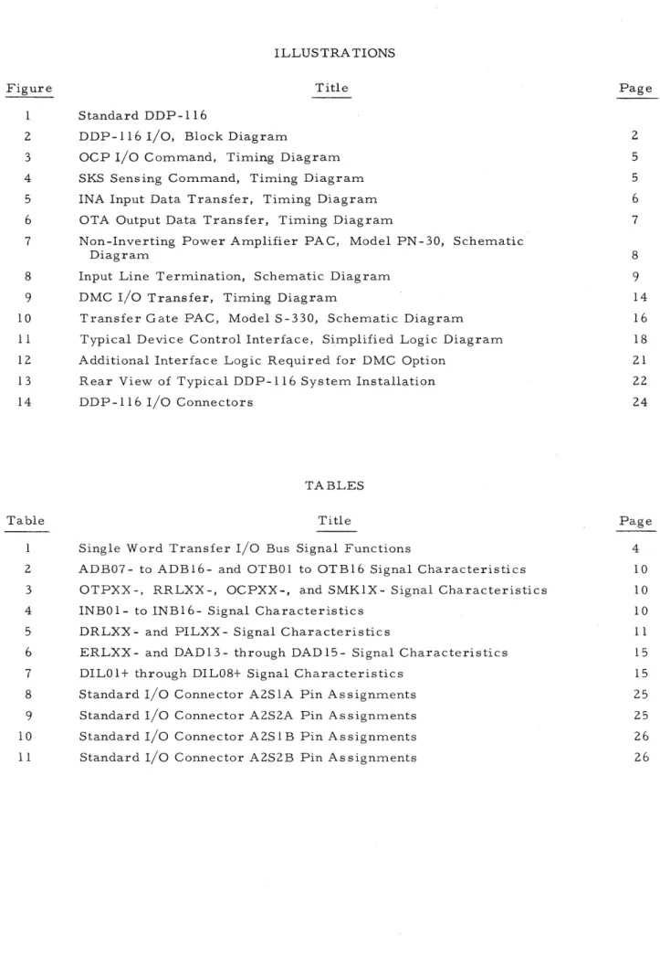
The DDP-ll6 General-Purpose Computer (Figure l) features versatile input/output capabilities, easy expandability through modular design, a variety of input/ output modes, and simplicity of operation. This manual describes and illustrates the interface character-istics of the DDP-ll6 to facilitate proper connection with peripheral equipment. The basic methods of input/output data transfer (Standard I/O Bus and Direct Multiplexed Channel) are described in sufficient detail for system planning purposes. Data and control lines required for input/output communications are defined, timing requirements are established, and in-terface gating drive and load requirements are specified. A detailed description of input/ output operation is given in the DDP-ll6 Programmer I s Manual.
DDP-116
II
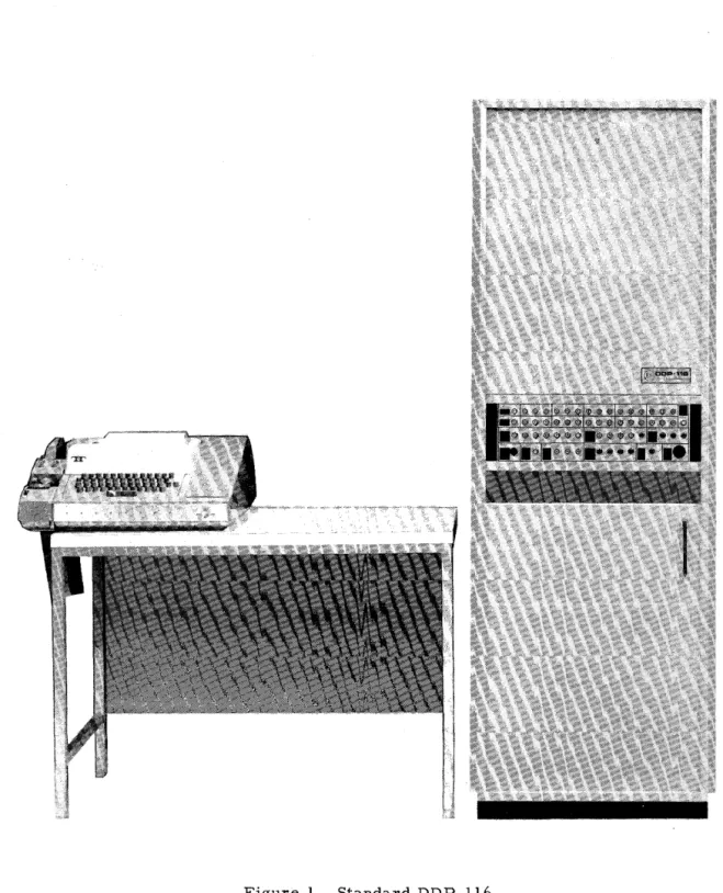
0 COMMUNICATIONCommunication links between the standard DDP-116 and its peripheral equipment are illustrated in Figure 2. The standard machine, without options, communicates with peripheral equipment on a parallel
r/o
bus under program control. A separate instruction is required for every input or output word transfer. All peripheral devices (up to 18 may be attached) are tied to a single interrupt signal line. When a device requests service through the interrupt line, a programmed subroutine determines which device requires service. An optional priority interrupt system is available to eliminate the need for programmed priority determination.The Direct Multiplexed Channel (DMC) option is a time- shared automatic
r/o
system that uses the parallelr/o
bus for communication but performs single character or block data transfers without program intervention. DMC transfers are interleaved with computa-tion; the starting and terminating addresses of the locations to which the block of informationis to be transferred are set up initially in standard memory locations under program control. Data transfers thereafter occur at a rate of one word every 6.8 microseconds. The transfer rate is over 145, 000 words per second. At slower
r/o
rates, any time not needed by the DMC is used for computation.in-N
,..-.--- --- -- --- - --- ---STANDARO-iioBUS
'
IK TO 32K COINCIDENT
CURRENT CORE MEMORY
A BUS
RLXX-I I I
I I
I
_____ 1 _ _
;_060_ ---
----t
ARITHMETICREG. (A,B, ADDER)
STANDARD I I I DDP-1I6 I MAIN FRAME : I
I
1 I '- ________ - _____________ - - - - _ _ _ _ _ _ _ _ - - ___ - _ _ _ _ .... _1
DMC STOPX DALOI
I I
1
DAL08-
ERLXX-OPTION I DILOI + I I I DIL08+
' - - - /
--TO ADDITIONAL DMC I/O DEVICE CONTROL INTERFACES
terfaces can be designed. The following information will enable a user to design any device or communication link control interface compatible with the DDP-116 bus structure, from the standpoints of timing, logic levels, and circuit loading.
STANDARD PARALLEL I/O BUS
Standard I/O Bus Lines
The standard DDP-116 input/output mode consists of transfers of single characters or 16-bit words to and from the data processor B bus. Input transfers are performed by INA instructions, and output transfers by OTA instructions. Communication with peripheral device s is accomplished by using an Input/Output Bus, consisting of the following elements: 10 address lines (ADB07 through ADBI6); 16 input data lines (INBOI through INBI6); 16 out-put data lines (OTBOI through OTBI6); and a series of control lines (OCP, SMK, RRL, OTP, DRL, and PIL). The data processor distinguishes between devices (with respect to the destination of commands or the source or destination of data transfers) by a six- bit binary code on the address bus. Up to 18 devices may be paralleled on the common bus.
Logic Levels
Standard logic levels for S-PAC circuits are 0 volt for logical ZERO and - 6 volts for logical ONE. Negative logic is used in DDP-116 I/O communication to permit ORing of
r/o
bus levels. All active signals (command pulses and binary ONE bits in data and address codes) are transmitted at the current-driving O-volt level. Binary ZEROs and quiescent control signals rest at the -6-volt level for minimum current drain.Timing of the address, data, and command lines from the DDP-116, and timing requirements imposed on responses from the device control units, are conditional upon the instruction in effect. Table I provides I/O bus line functions for the operational modes pe-culiar to I/O processing. Each of the modes is described in detail in the following paragraphs.
OCP Commands
OCP commands initiate motion of a device or prepare it for a specific mode of operation. No data is exchanged, and no response signal is expected from the addressed device. Only the address bus lines and the OCPXX-command pulse are involved. OCP command timing is shown in Figure 3.
The device addres s code and function code are gated from OCP instruction word positions 7 through 16 to the corresponding bit positions of the address bus. During the last half of the address interval, the OCPXX-command pulse occurs to enable the addressed , device to perform the control function specified by the function code portion of the addres s.
No direct response is required of the device. Any information placed by the device on DRLXX- or INBO I to INB 16 will be ignored by the computer during this instruction.
~
Table 1.
Single Word Tra nsfer I/O Bus Signal Functions
Control or Data Function
Line OCP SKS INA OTA Set Mask Interrupt
OTB
l_16 Contains data status code Contains mask
INB 1-16 Device applies
data ADB
7_10 Function code Function code Function code Function code Unique code ADB
ll_16 Device address Device address Device address Device address Unique code
OTP Strobes data to
device buffer
DRL Device replies Device replies Device replies
if condition de- if ready if ready termined by
function code is TRUE
RRL Resets device Resets device
ready flip-flop ready flip-flop OCP Sets mode
de-termined by function bits
SMK1 Strobes mask
bits to rna-sk flip-flops
PIL
Asynchro-nous signal originating in device I
'-'0'
ADB07- THROUGH ONE LEVEL (OV)
t
ADB 16 - (DEVICE GUARANTEED =:-1
ADDRESS AND AT I/O CONNECTOR 1L.. _ _ _ _ _ _ ZE_R_0_L_E_V_E_L...;.<-_6_V..;..,) _ _ _ - - J
FUNCTION CODE)
OCPXX-GUARANTEED I
AT I/O CONNECTOR I
I/O CONNECTOR TIME REFERENCE
1013 1210
tt
1980 2190 OV
11
-6V
NOTE: TIME INTERVALS ARE IN NANOSECONDS
Figure 3. OCP
r/o
Command, Timing DiagramINA, or OTA instruction cycle.
Typical uses of the OCP command are to:
a. turn the high- speed paper tape punch on or off,
b. set up the binary or BCD mode in the paper tape reader, and c. rewind magnetic tape.
SKS Commands
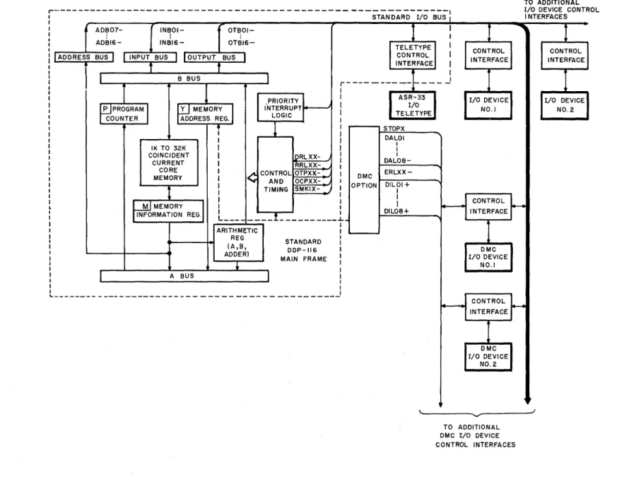
The SKS command is used to te st the condition of any device connected to the standard I/O bus. The command is implemented by gating the devices address onto the address bus with a function code that identifies the condition being tested. If the condition is true, the device interface must bring the DRLXX- line to the O-volt level during the time limits specified in Figure 4. The DRLXX- signal causes a program skip to the next in-struction in sequence. If the DRLXX- line remains quiescent, the next instruction in se-quence is executed.
ADB07-THROUGH ADB 16 - (DEVICE ADDRESS AND FUNCTION CODE)
DRLXX-2281 2455
GUARANTEED
~
ONE LEVEL (OV)t
t
AT I/O CONNECTOR 1~ _ _ _ ---Z-E-RO-L-E-V-E-L-(---6-V-)---~ __ J
I I REQUIREMENT I AT I/O CONNECTOR J
+
1045
MUST ARRIVE BY
1235
MUST REMAIN UNTIL
NOTE: TIME INTERVALS OV
-6V
I/O CONNECTOR ARE IN NANOSECONDS
TIME REFERENCE
INA Com=-"'a..1J.u.;:; -'~
An INA command addresses
a
particular device and senses the device condition.If the device replies with a "ready" indication, the input bus is strobed to the DDP-ll6 A reg-ister. Timing is illustrated in Figure 5. The address and function code are placed on the address bus. Within 1. 2 microseconds after receiving the address, the device must bring the DRLXX-line to the "ready" condition (0 volt level). Otherwise, the DDP-ll6 ignores the data on the lines and continues with the normal porgram. If the "ready" condition is detected, data on the input bus is strobed to the A register and the next instruction in sequence is skipped.
While data is being strobed into the A register, a reset ready pulse (RRLXX-) is sent out from the computer to indicate that the information has been accepted. This signal may be used to dc reset the ready flip-flop in the control interface. The device must apply data to the input bus within 2.3 microseconds after receiving the address.
ADB07- TH ROUGH ADBI6 -(DEVICE ADDRESS AND FUNCTION CODE)
DRLXX- (FROM DEVICE CONTROL)
RRLXX-INBOI-THROUGH INBI6-(FROM DEVICE CONTROL
o 3882 4055
GUARANTEED I ONE LEVEL (OV)
t-....
,t---ATI/OCONNEC~
~. ---~~ ZERO LEVEL(-6V) _ _ _ _ _ _ _ _ _ _ _ _ _ _ ~ _JI
I
REQUIREMENT I
AT I/O CONNECTOR I I I GUARANTEED I AT I,() CONNECTOR I
1045
MUST ARRIVE BY ~--MUST REMAIN UNTIL
2130 2926 3110
OV ~
: 1.618 1875
~. OV
-6V
REQUIREMENT --+I---~
AT I/O CONNECTO~ MUST ARRIVE BY~ MUST REMAIN UNTIL
+
-6VI/O CON N ECTOR
TI ME REFERENCE NOTE: TIME INTERVALS ARE IN NANOSECONDS
Figure 5. INA Input Data Transfer, Timing Diagram OTA Commands
During an OTA output command, the device address and data are applied to the address and output bus lines. The device's ready status is sensed and if the device is
pre-pared to receive the data, the OT PXX- pulse is generated to strobe the data to the device buffer. If the device is not ready, no strobing occurs, and the DDP-ll6 program continues on the assumption that the data transfer was not performed. Timing is illustrated in Figure 6.
3882 4055
ADBIS-(DEVICE GUARANTEED:-:-1
f--....;TJ---ADB07-THROUGH ONE LEVEL lOY)
t
1ADDRESS AN D AT I/O CONNECTOR~ , _ _ _ _ _ Z_E_R_O_L_E_V_E_L....;(_-_S_V..;.) _ _ _ _ _ _ _ _ _ _ _ _ - - - - . J
J
FUNCTION CODE) I 40 3255 3455
OTBOI-THROUGH OTBIS- (OUTPUT DATA WORD)
I ~ ~ •
GUARANTEED I
I
ONE LEVEL (OV) ;"I-_~J:---AT I/o CONNECTOR: _ ZERO LEVEL (-SV) _DRLXX-(FROM DEVICE CONTROL)
OTPXX-
RRLXX-I 1045 1235
I ~
t
REQUIREMENT I M S A ST EM IN UNTI AT I/O CONNECTOR . U T RRIVE BY MU R A L -SV
OV
I 19S0 2130 292~ fllo
I ~,
ov
~ t~G~U~AR~A~N~T~E~E~D~~~I---~!r~1
-svL
__ ',, _________________ _
~T I/o CONNECTOR I _ _ _ _ : 1973 2170 2940 3150
I
+ •
t
t
_G_U_AR~A_N~T~E~E~D~~~I _____________________ ~lr~1 L~l!
___
O_V _____________ __ AT I/O CONNECTOR I _ _ _ _t
-6V
SMKIX-I/O CONNECTOR TIME REFERENCE
NOTE: SMKIX- OCCURS AT THIS TIME I F ADDRESS BUS
CONTAINS MASK CODE 00208
TIM E IN T E R VA LS ARE IN NANOSECONDS
Figure 6. OTA Output Data Transfer, Timing Diagram
Within 1.12 microseconds after receiving the address, the device must respond by bringing the DRL line to the "ready" condition (0 volt level). Otherwise, the program con-tinues on the basis that data was not accepted. If a "ready" condition is detected, the DDP-116 responds with the OT PXX- pulse, which enables the device to strobe the output data lines to the device buffer. A reset ready pulse (RRLXX-) is sent out concurrently with the OTPXX- pulse. Its trailing edge may be used to reset the ready status of the device.
Standard Interrupt Provisions
Interrupt masks are set and reset by a variant of the OTA instruction, in which the device address and function code portion of the instruction word are replaced by the arbitrary code 0020
8. All devices respond to the code by monitoring the output bus, which contains a mask- setting code derived from the A register. If a device detects a binary ONE (0 volt level) in its preassigned position, a mask flip-flop is set, and the device can call for service on the PILXX- line. If a device detects a binary ZERO in its preassigned position, a mask flip-flop is res et. The PILXX- level diverts the DDP-116 to a priority- determining sub-routine that performs SKS interrogations in the order of priority until the busy channel is detected.
Timing of the mask-setting instruction is illustrated in Figure 6. The address lines and output bus are generated as in an OTA instru~tion. When the peculiar mask- setting code is specified in the instruction word format, the SMKIX- pulse is generated. No
Once the mask flip-flop is set, the device interface asynchronously requests inter-rupt service by raising the PILXX-line. The computer responds by issuing a series of SKS instructions encoded to detect the device causing interrupt. Each device interface must contain a decoder to sense the "SKS interrupt" command and respond on the DRLXX-line.
If a device is not inter·rupting, it returns a 0 volt level on the DRLXX- Hne (see Figure 4) to cause a program skip to an "SKS interrupt" for the next lower priority. If the device is interrupting, the DRLXX-line is held at the
-6
volt level during the SKS command, and the program counter can process the next sequential instruction, which will refer to a subrou-tine appropriate to the interrupting device.Gating Circuit Characteristics
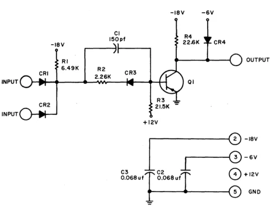
All data and control signals from the DDP-ll(> I/O bus to the device controls are driven by standard Computer Control Company type PN-30 non-inverting power amplifiers. (See Figure 7.) Each amplifier is capable of driving loads of up to a total of 96 ma maximum and up to 2000 pf in the power-driving state (0 vdc). Because several device interfaces may be connected in parallel on the
r/o
bus lines, it is recommended that no devicepresent a load of more than 2.4 ma at 0 volt to a given line. This particular require-ment can be disregarded in a special system application so long as the total current limit is not exceeded.
-lev SASK INPUT CRI INPUT CR2 NODE 8 CI 150PF R2 2.2SK CR3 R3 21.5K +12V -lev R4 1.33K QI R5 590 C2 390PF CR4 R4 11K +12V -lev R7 1.33K CR5 CR6
Figure 7. Non-Inverting Power Amplifier PAC, Model PN-30, Schematic Diagram
-sv R8 10 04 -sv CR7 C3 390PF
All input lines from device interfaces to the DDP-116 drive line terminations in a Special PAC. (See Figure 8.) These termination circuits operate as collector loads for th~
driving circuit and correspond to 3.2 ma at 0 volt. No external collector loads are to be used. Rise and fall times of input signal levels are not critical as long as the 90 percent and 10 percent levels occur within the time limitations shown in Figures 3, 4, 5, and 6.
Specifications for the
r/o
bus lines from the standpoint of a single device interface are summarized in Tables 2, 3, 4, and 5. For signals originating in the DDP-116, the in-formation is descriptive; it indicates what will be delivered to ther/o
connector panel. For signals originating at the device interface, the information is prescriptive; it indicates the limits to which the device interface must conform for compatibility with DDP-116 internal organization.r---,
INTERFACE
DRIVING SOURCE
L.. _ _ _ _ _ _ _ _
INPUT LINE
(DRL,INB, PIL,DIL)
r - - -
---I
I
I DDP-J16 " I
I J
I I
I I
I
I/O
CONNECTOR
r---,
I SPECIAL I
I PAC I
I I
I
750
-18 -6
I
I
I II
I
I
I
I
I I
L _ _ _ _ _ _ _ _ _ _ _ I I I
I
I~---~
Figure 8. Input Line Termination, Schematic Diagram
10
Table 2.
ADB07- to ADBl6- and OTBOl- to OTB16- Signal Characteristics
Binary ONE: Binary ZERO: Output loading:
Rise time:
Fall time:
Pulse specifications:
o
volt to -1. 5 volts - 5. 5 volts to - 6. 5 volts96 ma and 2000 pf maximum per line at ONE level Loading per device not to exceed 2. 4 ma per line at ONE level
200 ns from 10% to 90% points at DDP-116 I/O connector (nominal)
500 ns from 90% to 10% points at DDP-116 I/O connector (nominal)
See Figures 3, 4, 5, and 6·
Table 3.
OTPXX-, RRLXX-, OCPX.X-, and SMKIX- Signal Characteristics Active level:
Quiescent level: Output loading:
Rise time: Fall time:
Pulse specifications:
o
volt to -1. 5 volts - 5. 5 volts to - 6. 5 volts96 ma and 2000 pf maximum per line at active level
Loading per device not to exceed 2. 4 ma per line at active level
200 ns from 10% to 90% points at DDP-116 I/O connector (nominal)
500 ns from 90% to 10% points at DDP-116 I/O connector (nominal)
See Figures 3, 5, and 6.
Table 4.
INBO 1- to INB 16- Signal Characteristics Binary ONE:
Binary ZERO: Input loading by
DDP-116: Timing:
o
volt to -1. 5 volts -5.5' volts to - 6.5 volts3. 2 ma at ONE level for each line Negligible current at ZERO level
Table 5.
DRLXX- and PILXX- Signal Characteristics
Active level: Quiescent level: Input loading by
DDP-116 Timing:
o
volt to -1. 5 volts -5.5 volts to -6.5 volts3. 2 ma at active level for each line Negligible loading at quiescent level
For DRLXX-, see Figures 4, 5, and 6. Rise and fall time s are unimportant if overall timing is satisfied at DDP-116 I/O connector PILXX- is generated asynchronously by the device interface. Rise and fall times of less than 1. 5 Jlsec are recommended for optimum utilization of computer interrupt cycles
DIRECT MULTIPLEXED CHANNEL (DMC) OPTION
The DMC hardware option permits medium- speed and high- speed I/O transfers with a minimum of programmed control. Data transfers are performed by using the standard
r/o
bus and its control lines, but interrupts are initiated and I/O transfers are controlled by the DMC logic rather than by programmed INA or OTA instructions, When a device con-trolled by the DMC requests service, the DMC stops the program at the end of the current instruction and holds the computer in the D-state. During the D-state, a passive state dur-ing which normal computer cycles are suspended, the DMC performs a four-cycle simulated instruction that accomplishes the I/O transfer.During the four 1. 7 Jlsec cycles of the DMC sequence (G-cycle, H-cycle, J-cycle, and K-sync cycle), the DMC option assumes control of the computer memory and uses DDP-116 registers and the arithmetic capability to access or store data. The current pro-gram count and accumulator contents are preserved; at the end of the DMC sequence, the
computer is returned to the F- cycle of the next instruction unles s a new interrupt has occurred. Preas signed memory locations for each of the eight DMC channels must be set up wi th starting address minus one and end address, through normal programmed instructions. Devices must also be set up for the desired modes of operation by OCP commands, as in standard I/O trans-fers. Also, a device must be set up for DMC mode by a specialOCP, 03XX
S' Once these pre-liminary setups are made, I/O transfers occur on demand from the device, without program intervention.
is still in motion; if the computer assumed control for several cycles, data would be lost. Devices operating in the block transfer mode should be given the highest priorities; other-wise, other channels not in the block transfer mode might interrupt and cause data loss. When the block transfer mode has been set up for a particular channel, it is sustained until the channel reaches the end of range or is disabled by a stop command originating in the de-vice control interface. If a device runs out of data before the end of range is reached, the
stop command resets the block transfer mode in the DMC and permits the computer to resume control.
During normal computer operation, the DMC repeats its 1. 7 p,sec sync-cycle in synchronization with every computer cycle. If any of the eight channels becomes active during a sync-cycle, a priority evaluation is made and the highest priority is selected. The DMC is then ready to interrupt the computer, but the computer in turn permits DMC interrupt only during the last cycle of an instruction. If the computer does not accept the interrupt (for example, during the second cycle of a three- cycle instruction, such as OTA), the DMC is reset and a new priority determination occurs during the next sync-cycle. Thus it is possible for a device that was waiting for access during the unsuccessful sync-cycle to be superseded by a newer request from a device of higher priority.
When the interrupt demand is accepted, an address peculiar to the selected DMC channel is forced into the memory address register so that the memory cycle initiated as the last step of the instruction fetches the channel starting address rather than the next instruction word. The computer is arrested in the D- state, and the DMC, taking control, enters its G-cycle. During the G-cycle, the device is addressed and the starting location address is updated. An H-cycle follows, in which the end address is fetched. Next, a
J -cycle occurs, to perform the actual data transfer (using the standard I/O bus and appro-priate control lines). The final K-sync cycle repeats the function of the sync cycle and also compares the updated starting address with the end address. If they are identical, an end-of- range pulse is sent to the device to stop its oper ation. The K- sync cycle ends with a return of control to the computer, starting with the fetch cycle that was interrupted by the D-state. The DMC returns to its passive sync cycle until a new interrupt is sensed.
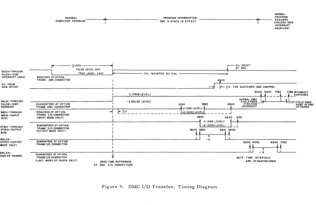
The basic control interfaces for DMC- controlled devices are logically identical to those used with the standard I/O bus, but additional logic must be added to accommodate the DAL address lines, DIL interrupt lines, ERLend-of-range line, andSTOPX- device stop line. The timing and the characteristics of these additional signals are described in the following paragraphs.
I/O Transfers
highest priority by enabling an address signal on the appropriate DAL line. The DAL signal appears on the address lines early in the DMC G-cycle; its leading edge establishes a zero time reference for all subsequent events.
Upon receiving the address, the requesting device interface inhibits its DIL line. Otherwise, the DIL line would remain high through the K- sync cycle and would erroneously enable a second DMC transfer to the same device.
For input transfers, data from the device must be placed on the input bus by T 1 of the DMC J -cycle and must remain through T3. It is conventional to reset input data by the end of the RRLXX-pulse, though data could be sustained through the end of the DMC sequence without conflict. The resetting of the device ready flip-flop by the RRLXX-pulse indicates that data has been accepted and that it is permissible to clear the buffer. The device ~IL
line is disabled as another consequence. The OTPXX-pulse is not generated by the DDP-116 during an input cycle, and the output bus remains inactive.
For output transfers, the device buffer must be clear by T3 of the DMC J-cycle. Data is applied to the output :bus during the time interval illustrated in Figure 9 and is strobed to the buffer by the OTPXX-pulse. The ready flip-flop is reset, and the PIL line is disabled by the RRLXX-pulse.
By the beginning of the DMC K-sync cycle, the input or output data transfer is com-plete, and the device interface is prepared for a new character. During the K-sync cycle, the updated data address is compared with the end address of the assigned block. If the end addres s has been reached, the DMC is inhibited from addressing data transfers to the device. A new priority determination is made, as during a sync cycle. The same device cannot cause a consecutive D- state, because its DIL line has been held off through the be-ginning of the K- sync cycle. If the DIL line of another device has been energized in time, however, the DMC retains control, the computer D- state is sustained, and another DMC transfer sequence occurs. If no new device is interrupting and the DMC is in time- sharing mode, control reverts to the computer for at least one full instruction cycle. In the block transfer mode, the D-state is sustained, DMC control remains in effect, and sync-cycles are repeated until an interrupt is detected.
When the end of range is detected during the K-sync cycle, the DAL line to the addressed device is sustained for an extra microsecond to gate the ERLXX- end-of-range pulse to the device controls, to turn off the "DMC ready" flip-flop. Because of the sus-tained address, no new interrupt is permitted even if a DIL line has been energized in time. Control is returned to the computer for at least one instruction cycle.
Special DMC Signal Gating Circuit Characteristics
*'"
DILOltTHROUGH DIL08t(DMC INTERRUPT LINES)
OIL FROM NEW DEVICE
DALOI-THROUGH DAL08-(DMC ADDRESS) INSOI-THROUGH INBI6-(lNPUT BUS) OTBOI- THROUGH OTBI6- (OUTPUT BUS) RRLXX-OTPXX~(OUTPUT
MODE ONLY)
ERLXX-(END OF RANGE)
NORMAL
COMPUTER PROGRAM -'-
T
PROGRAM INTERRUPTED:
..
I
DMC D-STATE IN EFFECT
NORMAL PROGRAM RESUMES (UNLESS NEW
INTERRUPT RECEIVED)
loil ;::1900
-I
_ _ _ _ _ ~ FALSE LEVEL (OV) . - - OIL RESET
TRUE LEVEL (-GV)
t
BY RRLREQUI RED AT OPTION FRAME DMC CONNECTOR
GUARANTEED AT OPTION FRAME DMC CONNECTOR
REQUIRED AT OPTION FRAME I/O CONNECTOR (INPUT MODE ONLY)
GUARANTEED AT OPTION FRAME I/O CONNECTOR (OUTPUT MODE ONLY)
GUARIiNTEED AT OPTION FRAME I/O CONNECTOR
GUARANTEED AT OPTION FRAME I/O CONNECTOR (LAST WORD OF BLOCK ONLY)
OIL INHIBITED BY DAL Ii
o (TRUE LEVEL)
- 6 (FALSE LEVEll
""1
r-
_~ ~____
-I
2930 3950
41
00-....I
:--;::0 FOR SUSTAINED DMC CONTROL6200 6400 7160 73B8 INTERRUPT
_ ~USTAINED
Ng~~NE~~~! l:::::::=: CYCLE ENDS 4840 IF NO NEW HERE AT END
INTERRUPT OF RANGE
,-Q \Lt;,.nv L.;I-VI...'-'j _ _ _ _ _ _ ..J 3845 4920 5155
o (ONE LEVEL) -6 (ZERO LEVEL) _J 3643 3850 4612 4840
~
__
~
____
~~H _~
t~1
______
~_
9
ZERO TIME REFERENCE AT DMC I/O CONNECTORS
Figure 9. DMC I/O Transfer, Timing Diagram
5865 6035 6843 7050
t
1 _
~
tL-L---1_
Table 6.
ERLXX- and DALOl- through DALOS- Signal Characteristics Active level:
Quiescent level: Output loading:
Rise time: Fall time:
o
volt to - 1 . 5 volts -5.5 volts to -6.5 volts96 rna and 2000 pf maximum per line at active level Loading per device not to exceed 2.4 rna per line at active level
200 ns from 10% to 90% points at option rack
110 connector (nominal)
500 ns from 90% to 10% points at option rack
110 connector (nominal) Pulse specifications: See Figure 9.
Table 7.
DILOI + through DILOS+ Signal Characteristics Acti ve level:
Quiescent level: Input loading by
DMC: Timing:
- 5. 5 volts to - 6. 5 volts
o
volt to -1 . 5 volts3. 2 rna at active level for each line Negligible loading at quiescent level See Figure
9.
DIL lines are generatedINPUT
CR2
INPUT
-18V
RI 6.49K
CI
150pf
R2
2.26K
+12V
-18V -6V
CR4
OUTPUT
QI
@-18V
r---0 -
6VFigure 10. Transfer Gate PAC, Model S-33 0, Schematic Diagram
PRIORITY INTERRUPT OPTION
The priority interrupt hardware option eliminates the need for a programmed sub-routine to identify the device requesting service. Identification is necessary because all device interface PIL lines are ORed to a common bus. In the priority interrupt option, PIL lines from up to eight different devices are applied to independent loads. When more than one interrupt demand occurs, the one having the highest priority is selected by prewired logie, .and a unique jump destination address is made available to the DDP-ll6. Synchro-nization is achieved during the next available computer fetch cycle, when the jump destin-ation is gated to the memory address register and a JST operdestin-ation code is forced into the F register. The computer proceeds as if an indirect JST instruction had been fetched. The destination, in this case, is the first program step of a subroutine suitable for I/O transfer to or from the interrupting device. The program count current at the time of the interrupt is retained, and when the I/O transfer is complete, the normal program is resumed. Sub-routines for interrupt I/O transfers may themselves be interrupted by a demand from a device of higher priority.
In order to initiate an interrupt demand, a device interface must first be enabled by the setting of its mask flip-flop, as described in connection with the standard I/O bus.
Priority interrupt option units may be used in multiple in a fan-in arrangement that accommodates up to 256 PIL lines and provides as many jump destination address codes.
Loading imposed on PIL lines by the priority interrupt option input gates is identi-cal to that imposed by the DDP-116.
TYPICAL DEVICE CONTROL INTERFACE
Simplified logic of a typical I/O device control interface is shown in Figure 11. The essential items are a group of address and function decoders, a ready flop, a busy flip-flop, a mask flip-flip-flop, an input/outputl
mode flip-flop, and a data buffer. Additional logic may be added as required to accommodate special device controls or format conversion.
OCP Commands
An OCP from the DDP-116 consists of a device addres sand f.unction code times with an OCP pulse. The interface address and function decoders respond to the OCP com-mand by energizing appropriate device control lines, to set up the specified operating con-dition. In the cas e of a command of the "write" type (a data output from the DDP-116), both the ready and busy flip-flops are set. The interface is prepared to accept data immediately. A command of the "read" type (a data input to the DDP-116) sets only the busy flip-flop; the ready flip-flop remains reset until the device drop-in pulse (DIP) has deposited data in the buffer register. An SKS instruction (or the SKS portion of an INA instruction) will then inform the DDP-116 that the input tr ansfer can be performed.
The mode flip-flop is set up according to the type of OCP in effect, to store an indication of the direction of data transfer.
SKS Testing
During an SKS cycle, the address bus addresses the device, and the function code bits specify the condition to be tested. In the illustrated example, independent gates test for SKS ready, SKS busy, and SKS interrupt. Other SKS gates may be added as required to test for special device conditions, such as "end of file." When an SKS condition is fulfilled, the DRLXX-line is brought to 0 vdc.
Standard Input Data Transfers
00 110 BUS DDP-116 DRLXX- MSTCL- NCOXX- AD~07- ADEII6-
OCPXX-, - - - 1
I DEVICE INTERFACE I
I , _ , 1
1
1 1
NCO L,--,-J L,----,J L.,-,-l / 1 RE A DY 1
READy-l
I
BUSY~I
I
~r-
IADDRESS AND FUNCTION DECODERS OCP
STANDARD ADDRESS OUTP~ .... ~
I
1
PILXX- - - I OCP
" • DMC i ADDRESS \ I/O
DEVICE
OTHER PIL LINES OR'ED
RRLXX- SMKIX- OTPXX- OTBOI- OTBI6- INBOI- INBI6PARCH -RRL RRL MASK READY r---MASK SET r----MASK SET DA STOP MOTION COMMAND BUSY
BUSY RRL INPUT OCP
MODE
READY
DiP
• " IDROP-IN·PULSE
NCO OTB N Di:P OCP DA
BUFFER (TYPICAL OF BITS 1-16)
L _ _ _ _ _ _ _ _ _ _ _ _ _ _ _ _ _ _ _ _ _ _ _ _ _ _ _ _ _ _ _ _ _ _ _ _ _ _ _ _ _ _ _ ...I
Figure 11. Typical Device Contr 01 Interface, Simplified Logic Diagram
INPUT DATA
OUTPUT DATA
and the ready flip-flop are reset in preparation for another cycle. Input transfers continue as long as the device is operating and INA instructions recur.
Standard Output Data Transfers
During the fir st of a series of OTA instructions, the ready flip-flop will be set, and the SKS test performed as part of the instruction will be satisfied. The first data word is strobed into the device buffer by the OTP pulse. The input/ output mode flip-flop, set to the output mode condition by a previous OCP, prevents resetting of the buffer by the RRLXX-pulse. The resetting of the ready flip-flop by the trailing edge of the RRLXX-pulse renders the device exempt from I/O transfers until the character in the buffer has been taken during the device load pulse (DLP). The trailing edge of DLP again sets the ready flip-flop, after which another word can be loaded by the next OTA cycle.
Setting Mask Flip- Flop
Mask flip-flops for all devices on the standard I/O bus are set up simultaneously by a unique instruction that gates a mask code on the output bus and produces the SMKl X-pulse. Each device is as signed one output bus line; if that bit contains a binary ONE, the mask flip-flop is set; otherwise the mask flip-flop is reset. Note that the mask set instruction may be used to prevent interrupts as well as enable them.
Standard Interrupt for Input
After an OCP has enabled a device to provide input data to the DDP-116, the com-puter may continue with the normal program until the device drop-in pulse (DIP) delivers the first word to the buffer and sets the ready flip-flop. The ready condition, gated with the set output of the mask flip-flop, energizes the PILXX-line. The energization of the PILXX-line forces the program to jump to a priority subroutine in which SKS interrupt instructions are addressed to the various peripheral devices in the order of priority. (Meanwhile, the interrupting device holds the data ready in, the interface buffer.) An SKS interrupt command addressed to the active device is decoded and gated with MASK SET and READY. A nega-tion on the DRLXX-line permits the DDP-l16 to undergo a program jump to an INA instruc-tion that will accept the data and reset the ready flip-flop. The next droop_in pulse again sets the ready flip-flop, and the cycle is repeated.
Standard Interrupt for Output
addressed to the active device is decoded and gated with MASK SET and READY. An asser-tion on the DRLXX-line permits the DDP-116 to undergo a program jump to an OTA instruc-tion that will strobe data to the device buffer and reset the ready flip-flop. Removal of the ready condition deenergizes the PILXX-line. The device thus remains exempt from OTA data transfers until the device load pulse (DLP) takes the data and sets the ready flip-flop. The PILXX-line is again energized and another interrupt cycle is requested.
System Normalize
Two lines from the computer place the device interface in a normal starting con-dition. The MSTCL-level is produced whenever the MASTER CLEAR button is pressed; the NCOXX- system normalize pulse occurs for 100 milliseconds at the beginning of every power-on cycle. Both signals are ORed in the interface and converted to the NCO level, which resets the busy, ready, and mask flip-flops.
Special DMC Provisions
Device interfaces may optionally be provided with subchannel logic for operation under DMC control. The required additions are a DMC enable flip-flop and control logic to produce the DILXX- DMC interrupt line. These eleITlents are shown in Figure 12.
In DMC operation, the DMC address is used in lieu of the standard address to prepare the interface for a data tr ansfer, either input or output. A DMC enable flip-flop, set by a special OCP cOITlITland, enables DMC interrupt requests on the DILXX+1ine. When
an ERLXX- end-of-range signal froITl the DMC option has reset the DMC ready flip-flop, DMC interrupts are not perITlitted.
Except for these provision$, DMC data transfers occur in the saITle ITlanner and use the saITle I/O and control lines as the standard I/O bus.
Devices capable of block transfers ITlust also have provisions for connection to the STOPX-line which resets the DMC block transfer control flip-flop when a device has run out of data before the end of range has been reached. Otherwise, the DMC would retain con-trol and wait for nonexistent data.
Parity Check Input
A parity error signal input line, PARCH-, is provided on an I/O connector so that devices with parity check logic can light the parity error indicator on the DDP-116 control panel. To energize the indicator, a - 6- volt input level is required.
SYSTEM INTERCONNECTING DATA
A typical expanded DDP-116 installation involving aITlain fraITle and satellite cabi-net is shown in Figure 13. When rack-ITlounted devices are supplied as an integral part of an option cabinet, all interconnections are wire-wrapped upon initial asseITlbly; no cabling is necessary.
DMC OPTION
r
-I
~--S-T-O-P-X----~I---(STOP
COMMAND FROM DEVICE)*
DA~OI-I
DALo8-DA
OCPXX-- - - + I
ERLXX-DILXX+
L- _ _ _
'*
ONE DAL LINE ASSIGNED TO EACH DEVICE-
-
-
--.,
--~,
,:'::: p-- ..
DAl ~ .... I _ _
I
DMCI ADDRESS
BUSY
READY
1
I
l
I
I
I
I
I
I
- - - 'Figure 12. Additional Interface Logic Required for DMC Option
I/O bus communication from cabinet to cabinet is by means of umbilical I/O cables. Such cables are permanently wired to an option cabinet at one end; the other end is equipped with plugs that match standard I/O connector jacks. Any number of option cabinets may be inter connected in this manner.
Eight additional control lines, ACKOl- through ACK08-, are provided to reset interrupt control flip-flops in devices that do not contain a ready flip-flop. (The Real Time Clock option is such a device.) Devices that are not involved in data transfers never
receive INA or OTA commands and thus do not receive the RRLXX-pulse that resets the ready flip-flop and disables the PIL line.
N N
TELETYPE SIGNAL ASR DATA ASR-18V
I
DATA LINE CONNECTION
TELETYPE POWER DISTRIBUTION TERMINAL BOX TERMINAL
TBI-6 A2CIB-4 TBI-7 A2CIB - 6
~~
ASR-33TELETYPE
l
U
POWER
DATA
DDP-116 MAIN FRAME
AC STRIP (3:DlWIREMOLD
I/O CONNEClOR PANEL
I ...
POWER..r-t .
¢J
~ DISTRIBUTION~ CJ
UMBILICAL
OPTION CABI NET
rrrr
rffr
IIO CONNECTOR PANEL ~ c:::J t CJ CJ f--c::Jc::Jc:::Jc::Jc::JUMBILICAL fT1 OPTIONAL CONNECTOR
SATELLITE OPTION CABINET
DEVICE CONTROL
8-INTERFACE t
-llll 1111
IIO CONNECTOR PANELc:::J c::J CJ t c::J CJ
c:::J CJ CJ c::J CJ
~
Figure 13. Rear View of Typical DDP-116 System Installation
load limit is 2.4 rna at 0 volt. The lines are brought to the negation level (0 volt) for approximately 2.0 fJ.sec during the interrupt JST instruction cycle.
Interconnecting Cables
Interconnecting cables between the DDP-116 and peripheral equipment will vary in length according to the placement of the units with relation to each other. Maximwn length of signal cables should be SO ft. 1£ cable lengths are specified in the contract, cables of the specified length will be provided with the equipment. If the cables are to be as sembled at the installation site, mating plugs are provided for the receptacles of the connector panel.
A IS-it power input cable is provided with each DDP-116 system. It is normally taped within the equipment for storage during shipment.
Power and data cables are supplied with the ASR -33 Teletype. The power cable plugs in to the main frame wiremold ac strip. The two-wire data cable attaches to a terminal block on the ASR-33.
I/O Connectors
The DDP-116 is equipped with a comprehensive connector panel, located behind the hinged ac power distribution chas sis at the rear of the main ~nclosure. (See Figure 14. ) All connector s on the panel are identical. Three (A2SlA, A2S2A, and A2S1 B) are perma-nently allocated as I/O connectors, with the I/O bus pin assignments listed in Tables 8, 9, and 10. Another connector, A2S2B,(Table 11), isprovidedforcontrollinesusedwiththepriority interrupt option. Remaining connector cutouts on the panel are for connectors required by special systems. Information on special connector pin assignments will be supplied as required.
Extension and satellite enclosures are identically equipped with a standard connec-tor panel.
AC Power Distribution
AC line power is distributed within the standard DDP-116 through a wiremold receptacle strip running the vertical length of the cabinet. Power supplies, blowers, and other devices requiring line power are converted directly into the strip. Prime power is controlled by circuit breakers and contactors in the power distribution box.
DC Power Distribution
N
~
AC POWER RECEPTACLE
DC GROUND RECEPTACLE
0 0 0 0 0 0 0 0 0 0 0 0 0 B 0 F 0 LOR 0 V 0 Z 0 hOY 0 EO!!. 0 't. 0 CCoHH
o J N T X b f m ! ~ AA EE
0 0 0 0 0 0 0 0 0 0 0 0 0
A E K P U Y £ j n t ! BB FF 0 0 0 0 0 0 0 0 0 0 0 0 C H M S W a k ~ ~ DO
~
~
STANDARD I/O CONNECTOR (WINCHESTER MRAC - 50S)
POWER DISTRIBUTION PANEL
CONVENIENCE OUTLETS
Figure 14. o
oL.-ELAPSED TIME METER
o
DDP-116
II
0 Connectors
System Grounding
AC power ground is brought into the DDP-116 enclosure in the main power cable. DC power ground is distributec:l within the enclosure by a copper comb running along the bottom of each S-BLOC. A common dc ground is maintained from cabinet to cabinet by using the dc ground connector, A2B2D.
Table B.
Standard I/O Connector A2SIA Pin Assignments
Table 9.
Standard I/O Connector AZS2A Pin Assignments
Pin Function Pin Function Pin Function Pin Function
A OTBOl- e OTB14- A INB01- e
INB14-f
B OTBOl-GND f OTB14-GND B INBOl-GND f INB14-GND
C OTBOZ- h, OTB15- C INBOZ- h
INB15-D OTBOZ-GND
L
OTB15-GND D INBOZ-GND.i.
INB15-GNDE OTB03- k OTB16- E INB03- k
INB16-F OTB03-GND m OTB16-GND F INB03-GND m INB16-GND
H
OTB04- n DRLXX-H
INB04- nJ OTB04-GND
E
DRLXX-GND J INB04-GNDE
K OTB05- r K INB05- r
OTPXX-L OTB05-GND s L INB05-GND s OTPXX-GND
-
-M OTB06- t M INB06- t
RRLXX-N OTB06-GND -u N INB06-GND -u RRLXX-GND
P OTB07- I
v P INB07- v
OCPXX--
-R OTB07-GND w R INB07-GND w OCPXX-GND
-
-S OTBOB- x S INBOB- x PILXX+
-
-T OTBOB-GND
X.
T INBOB-GNDX.
PILXX+GNDU OTB09- z U INB09- z
SMKIX--
-V OTB09-GND AA V INB09-GND AA SMKIX-GND
W OTBIO- BB W INBIO- BB
SMKZX-X OTBIO-GND CC X INBIO-GND CC SMK2X-GND
y OTB 11- DD y INBll- DD
SMK3X-Z OTBll-GND EE Z INBII-GND EE SMK3X-GND
a OTBlZ- FF a INBIZ- FF
SMK4X-b OTBlZ-GND
HH
b INBIZ-GNDHH
SMK4X-GNDc OTB13- c
INB13--
Table 10. Table 11.
Standard I/O Connector A2S 1 B Pin As signments 'Standard I/O Connector A2S2B Pin As signments
Pin Function Pin Function Pin Function Pin Function
A ADB07- e DIL04+ A DALOI- e
ACKOS-B ADB07-GND f DIL04+GNp B DALOI-GND f ACKOS-GND
C ADBOB- h DILOS+ C DAL02- h
ACK06-D ADBOB-GND
i
DILOS+GND D DAL02-GNDi
ACK06-GNDE ADB09- k DIL06+ E DAL03- k
ACK07-F ADB09-GND m DIL06+GND F DAL03-GND m ACK07-GND
H ADBIO- n DIL07+ H DAL04- n
ACKOB-J ADBIO-GND
E
DIL07+GND J DAL04-GNDE
ACKOB-GNDK ADBll- r DILOB+ K DALOS- r PILOl+
L ADBII-GND -s DILOB+GND L DALOS-GND s PILOl+GND
-M ADB12- t M DAL06- t PIL02+
N ADB12-GND
-
u N DAL06-GND u PIL02+GND
-P ADB13-
-
v P DAL07- v PIL03+
-R ADB13-GND
-
w R DAL07-GND w PIL03+GND-S ADB14- x PARCH- S DALOB- x PIL04+
-
-T ADB14-GND
Y
PARCH-GND T DALOB-GND Y PIL04+GNDU ADBlS-
-
z ERLXX- U z PILOS+
-V ADBIS-GND AA ERLXX-GND V AA PILOS+GND
W ADB16- BB MSTCL- W ACKOl- BB PIL06+
X ADB16-GND CC MSTCL-GND X ACKOI-GND CC PIL06+GND
Y DILOl+ DD NCOXX- y ACK02- DD PIL07+
Z DILOl+GND EE NCOXX-GND Z ACK02-GND EE PIL07+GND
a DIL02+
FF
STOPX- a ACK03- FF PILOB+b DIL02+GND HH STOPX-GND b ACK03-GND HH PILOB+GND
c DIL03+ c
ACK04--
-d DIL03+GND d ACK04-GND