Differential Precision Rectifier using Single CMOS DVCC
Ahmed M. Nahhas
Department of Electrical Engineering, Faculty of Engineering and Islamic Architecture, Umm Al Qura University, Makkah, Saudi Arabia
ABSTRACT
Three novel differential precision rectifier circuits are realized using single CMOS differential voltage current conveyor. One of the realized differential precision rectifiers provides half wave voltage output. The other two circuits give full wave voltage outputs. Among the two full wave differential precision rectifiers, one circuit provides single ended voltage output while other full wave differential precision rectifier gives differential full wave voltage output. All the realized differential precision rectifiers possess the gain control facility through two resistors ratio. The realized differential precision rectifier circuits are designed and verified using PSPICE and the results thus obtained justify the theory.
Keywords
Current conveyors, DVCC, precision rectifiers.
1.
INTRODUCTION
For over last two decades the current conveyors have been dominating in the area of analog signal processing due to their functional versatility in addition to higher signal bandwidth and greater linearity. As a result vast variety of linear and nonlinear analog signal processing applications are reported in technical literature [1-32].
Among nonlinear analog signal processing applications the precision rectifiers form an important building block. In such rectifiers, the threshold voltages associated with diodes are overcome and hence enable the rectification at relatively low signal levels required for signal processing applications. With the advent of current conveyors, which offer a number of advantages over other devices, many precision rectifiers using current conveyors have been recently reported in literature [21-32]. However, many of them use a complex circuitry and provide only single ended input and output.
In this paper three new differential precision rectifier (DPR) circuits are presented using only single differential voltage current conveyor (DVCC) along with one or two CMOS pair. One of the realized differential precision rectifiers provides half wave voltage output. The other two circuits give full wave voltage outputs. Among the two full wave circuits, the first one provides differential precision rectifier with single ended output (DPRSO), while other full wave differential precision rectifier gives differential output (DPRDO). All the realized differential precision rectifiers possess the gain control facility through two resistors ratio. The realized differential precision rectifier circuits are designed and
verified using PSPICE and the results thus obtained justify the theory.
2.
THE CMOS DVCC
The differential voltage current conveyor (DVCC) symbol is shown in “Figure 1(a)” and its CMOS implementation with two Z+ and one Z- outputs is shown in “Figure 1(b)”. The transfer matrix of the DVCC can be expressed as
Z Z X Y Y Z Z X Y YV
V
I
V
V
I
I
V
I
I
2 1 2 10
0
1
0
0
0
0
1
0
0
0
0
0
1
1
0
0
0
0
0
0
0
0
0
0
(1)Thus the port voltages and currents for the DVCC can be expressed as X Z X Z Y Y X Y Y
I
I
I
I
V
V
V
I
I
2 1 2 10
(2)The additional number of Z+ or Z- outputs may be added as per requirement just by connecting in parallel a set of PMOS and NMOS for each output as shown in “Figure 1(b)”.
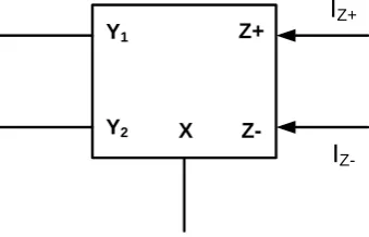
Y1
Y2
Z-Z+
X
I
Z+I
[image:1.595.339.509.570.679.2]X Z+ VDD
VSS
M3 M4
M5 M6
Y1
Y2
VB B
M1 M2
M9 M10
M7
M11
M8
Z-M12
M13
M16
M14 M15
M17 M18
Z+
M20
M19
Fig 1(b): The CMOS implementation of a DVCC with two Z+ and one Z- outputs
3.
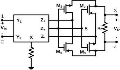
THE DPR CIRCUITS
The three new differential precision rectifiers using single DVCC are given in “Figure 2” where the forced current into high gate resistances saturates the voltage at the node 5, which is enough to switch ON or switch OFF the MOSFET switches M1 through M4. The circuit of “Figure 2(a)” gives half wave
differential precision rectifier with two different outputs. In “Figure 2(a)” during positive cycle the NMOS switch M1 is
ON and the positive cycle current passes through resistor R2 at
node 3 while during negative cycle M1 is OFF and hence there
will be no current through R2. Thus the half wave rectified
voltage output is available at node 3. Similarly, during positive cycle M2 is OFF and so no current through R3 at node
4 while during negative cycle M2 is ON and thus the inverted
negative cycle current from Z- terminal of the DVCC passes through resistor R3 at node 4 which results in the half wave
rectification at node 4. Thus at node 3 only positive half wave rectified voltage output is available while at node 4 inverted negative half wave rectified output voltage is present.
1
2
Vin
+
-Y1
Y2
Z+
Z+
Z
-R1
R3
R2 4 5
M1
M2
3
VDC
+
-VDC
+
-Fig 2(a): The HW differential precision rectifier circuit
The routine analysis yields its magnitude of output DC voltage at node 3 as well as at node 4 as follows.
1 2
)
(
R
R
V
V
miDC
(3)Where Vmi is the peak of the input AC voltage.
In “Figure 2(b)” also during positive cycle the NMOS switch M1 is ON and PMOS switch M2 is OFF and thus the positive
cycle current passes through resistor R2 at node 3. While
during negative cycle M1 is OFF and M2 is ON and thus the
inverted negative cycle current also passes through resistor R2
in same direction and results the full wave rectification. Thus the circuit of “Figure 2(b)” gives full wave differential precision rectifier with single ended output and its output DC voltage at node 3 can be expressed as
1 2
)
2
(
R
R
V
V
DC mi
(4)Y1
Y2
Z+
Z+
Z
-R1
R2
X
M1
M2
1
2
Vin
+
-3
VDC
+
-5
Fig 2(b): The FW differential precision rectifier circuit with single output-DPRSO
Y1
Y2
Z+
Z+
Z -X
R2
M1 M2
M3 M4
VDC +
-Vin
+
-1
2
3
4 5
[image:2.595.137.464.75.263.2] [image:2.595.333.526.407.564.2] [image:2.595.79.258.506.612.2] [image:2.595.332.529.608.724.2]In “Figure 2(c)” during the positive cycle the NMOS switches M1and M3 are ON while PMOS switches M2 and M4 are OFF
and thus the positive cycle current passes through resistor R2.
During negative cycle the NMOS switches M1and M3 are
OFF while PMOS switches M2 and M4 are ON and thus the
inverted negative cycle current also passes through resistor R2
in same direction and results the full wave rectification. Thus the circuit of “Figure 2(c)” gives full wave differential precision rectifier with differential output and its output DC voltage is same as given in equation (4). It is to be noted that the ON resistance of the CMOS switches is low at signal magnitude [20]. In precision rectifiers as the signal magnitude is significantly small, the switch resistances may play insignificant role.
Taking the tracking errors of the DVCC into account, the relationship of the terminal voltages and currents of the DVCC can be rewritten as
X Z
X Z
Y Y
X Y Y
I
I
I
I
V
V
V
I
I
)
(
0
2 1
2 1
(5)
where, β is the voltage transfer gain from Y to X terminal and α is the current transfer gain of the DVCC from X to Z terminal. The above transfer gains slightly deviate from unity and the deviations are quite small and technology dependent [14]. By including these non-ideal effects the DVCC the DC output of the HW-DPR given in equation (3) is modified as
1 2
)
(
R
R
V
V
miDC
(6)Similarly, the DC output of the full wave DPRSO as well as for DPRDO given in equation (4) is changed to
1 2
)
2
(
R
R
V
V
miDC
(7)Thus, from equation (6) and (7) it is observed that the magnitude of the DC outputs of the DPR may get slightly affected due to non idealities of the DVCC. However, this reduction in gain may easily be adjusted through two resistors ratio.
4.
DESIGN AND VERIFICATION
The realized differential precision rectifiers of “Figure 2” were designed and verified by performing PSPICE simulation with supply voltage ± 1.5 V, using CMOS TSMC 0.25 μm technology parameters. The aspect ratios used are given in the Table 1. All the DPR were designed for unity gain with R1 =
R2 = R3 = 100 Ω. The observed wave shapes of the designed
[image:3.595.319.535.105.511.2]HW-DPR of “Figure 2(a)” and FW-DDPSO of “Figure 2(b)” are respectively, shown in “Figure 3” and “Figure 4”. The
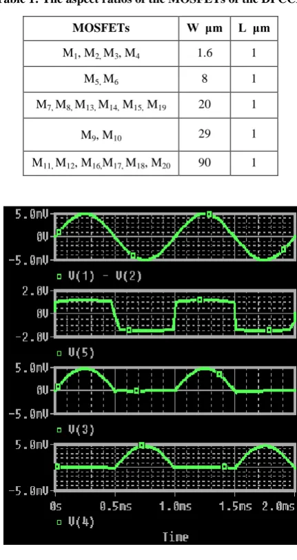
Table 1: The aspect ratios of the MOSFETs of the DPCCII
MOSFETs W μm L μm
M1, M2, M3, M4 1.6 1
M5, M6 8 1
M7, M8, M13, M14, M15, M19 20 1
M9, M10 29 1
[image:3.595.98.217.272.357.2]M11, M12, M16,M17, M18, M20 90 1
Fig 3: The differential input and differential output of the HW-DPRSO at 1 KHz
[image:3.595.318.540.535.734.2]observed wave shapes of the designed FW-DPRDO of “Figure 2(c)” are given in “Figure 5” at 1 KHz, 100 KHz and 1 MHz . To demonstrate the gain capability, the DPRDO of “Figure 2(c) was designed for a gain of 100 by selecting R1 =
0.3 KΩ and R2=30 KΩ. The observed wave shapes at 10 KHz
are shown in “Figure 5(d)”. The observed DC transfer characteristics of the DPRDO is given in “Figure 6” which shows a high degree of linearity and equal swing for both positive and negative variations of signal amplitude. Thus the observed results of “Figure 3” through “Figure 6”, show the close conformity with the theory.
Fig 5(a): The differential input and differential output of the DPRDO at 1 KHz
Fig 5(b): The differential input and differential output of the DPRDO at 100 KHz
5.
COMPARATIVE STUDY
An exhaustive comparison of various precision rectifiers is given in reference [32]. Here the novel precision rectifiers presented in this paper are compared with the precision rectifiers of reference [32] and the comparative results are given in the Table 2. The comparative results show that the proposed differential precision rectifiers use lesser number of active and passive components and provide the differential input in all the three cases, while the proposed circuit of “Figure 2(c)” provides the differential input as well as differential output.
Fig 5(c): The differential input and differential output of the DPRDO at 1 MHz
[image:4.595.318.540.71.251.2]Fig 5(d): The differential input and differential output of the DPRDO at 10 KHz and gain of 100.
[image:4.595.57.279.205.388.2] [image:4.595.319.540.296.517.2] [image:4.595.58.280.440.614.2] [image:4.595.319.541.562.736.2]6.
CONCLUSION
Three novel differential precision rectifier circuits are presented using single CMOS differential voltage current conveyor. One of the realized differential precision rectifiers provides half wave voltage output. The other two circuits give full wave voltage outputs. Among the two full wave circuits, the first one provides differential precision rectifier with single ended output, while the other full wave differential precision rectifier gives differential output. All the realized differential precision rectifiers use low component counts and possess the gain control facility through two resistors ratio. The effects of non ideal gains of the differential voltage current conveyor on the differential precision rectifiers are also studied. The realized differential precision rectifier circuits are designed and verified using PSPICE and the results thus obtained justify the theory.
7.
REFERENCES
[1] Wilson, B. 1990, Recent developments in current conveyors and current-mode circuits, IEE Proceedings G, Vol. 137, 2, 63–77.
[2] Toumazou, C., Lidgey, F. J. and Haigh, D. G. 1998, Analogue IC Design: The Current-Mode Approach, IEE, York, UK.
[3] Khan, I. A. and Maheshwari, S. 2000, Simple first order all-pass section using a single CCII, International Journal of Electronics, Vol. 87, 3, 303-306.
[4] Khan, I. A. and Zaidi, M. H. 2000, Multifunctional translinear-C current-mode filter, International Journal of Electronics, Vol. 87, 9, 1047–1051.
[5] Mita, R., Palumbo, G. and Pennisi, S. 2003, 1.5-V CMOS CCII+ with high current-drive capability, IEEE Trans. CAS-II, Vol. 50, 4, 187-190.
[6] Minaei, S., Ibrahim, A. Muhammed and Kuntman, H. 2003. DVCC based current-mode first order all-pass filter and its application. In Proceedings of The 10th IEEE International Conference on Electronics Circuits and Systems, Turkey, 276-279.
[7] Kumar, V., Keskin, A.U., Pal K. 2005, DVCC based single element controlled oscillators using all grounded components and simultaneous current voltage mode outputs, Frequenz, vol. 59, 7–8.
[8] Khan, I. A., Beg, P. and Ahmed, M. T. 2007, First order current mode filters and multiphase sinusoidal oscillators using MOCCIIs, Arabian, Journal of Science and Engineering, Saudi Arabia, Vol.32, 2C, 119-126.
[9] Tsukutani, T. Sumi, Y. and Yabuki, N. 2007, Novel current mode biquadratic circuit using only plus type DO-DVCCs and grounded passive components, International Journal of Electronics, vol. 94, 12, 1137– 1146.
[10] Sumi, Y. Tsukutani, T. and Yabuki, N. 2008, Novel current-mode biquadratic circuit using only plus type DO-DVCCCs, in Proceedings of the International Symposium on Intelligent Signal Processing and Communication Systems (ISPACS ’08), vol. 8–11, 1–4.
[11] Khan, I. A. and Beg, P. 2009, Fully differential sinusoidal quadrature oscillator using CMOS DVCC, Proc. International Conference on Communication, Computers and Power –ICCCP2009, Muscat, Oman, SQU-2009 ISSN: 1813-419X-101.1-101.3.
[12] Minaei, S. and Ibrahim, M. A. 2009, A mixed-mode KHN-biquad using DVCC and grounded passive elements suitable for direct cascading, International Journal of Circuit Theory and Applications, Vol. 37, 7, 793–810.
[13] Ansari, M. S. and Khan, I. A. 2010, Multiphase differential sinusoidal oscillator based on DVCC, Int. J. of Recent Trends in Engineering and Technology, Vol. 4, 3, 96-99.
[14] Chaturvedi, B. and Maheshwari, S. 2011, Current mode biquad filter with minimum component count, Active and Passive Electronic Components, Vol. 2011, 1-7,
[15] Khan, I. A. and Simsim, M. T. 2011, A Novel Impedance Multiplier using Low voltage Digitally Controlled CCII, Proc. IEEE GCC Conference and Exhibition, Dubai, UAE, 331-334.
[16] Khan, I. A. and Nahhas, A. M. 2012, Reconfigurable voltage mode first order multifunctional filter using single low voltage digitally controlled CMOS CCII, International J. Computer Applications, Vol. 45, 5, 37-40.
[17] Khan, I. A. and Nahhas, A. M. 2012, Current mode programmable analog modules using low voltage digitally controlled CMOS CCII, International J. Computer Applications, Vol. 48, 4, 38-44.
[18] Khan, I. A. and Nahhas, A. M. 2012, Reconfigurable voltage mode phase shifter using low voltage digitally controlled CMOS CCII, Electrical and Electronic Engineering, Vol. 2, 4, 226-229.
[19] Nahhas, A. M. 2012, Reconfigurable current mode programmable multifunctional filter, International J. on Recent Trends in Engineering and Technology, Vol. 7, 2, 88-91.
Reference No. No. of
Devices
No. of
Resistors HW/FW
Operating Frequency
Gain Facility
Type of Input/Output
Reference[32] (Fig.4)
2 CCII,
1 MOSFET 4 Yes/Yes 1MHz No Single Ended/Single Ended
Reference[32] (Fig.6)
2 DVCC,
1 MOSFET 3 Yes/Yes 1MHZ No Single Ended/Single Ended
Proposed Fig. 2(a)
1 DVCC,
2 MOSFET 2 Yes/No 1MHz Yes Differential/Single Ended
Proposed Fig. 2(b)
1 DVCC,
2 MOSFET 2 No/Yes 1MHZ Yes Differential/Single Ended
Proposed Fig. 2(c)
1 DVCC,
[image:5.595.75.533.93.244.2]4 MOSFET 2 No/Yes 1MHz Yes Differential/Differential
[20] Zumbahlen, H. 2006, Basic Linear Design, Analog Devices.
[21] Toumazou, C., Lidgey, F. J., and Chattong, S. 1994. High frequency current conveyor precision full-wave rectifier. Electronics Letters, Vol. 30, 10, 745-746.
[22] Gift, S. J. G. 2000. A high-performance full-wave rectifier circuit. International Journal of Electronics, Vol. 89, 467-476.
[23] Monpapassorn, A., Dejhan, K. and Cheevasuvit, F. 2001, A full-wave rectifier using a current conveyor and current mirrors, International Journal of Electronics, Vol. 88, 751-758.
[24] Tiliute, D. E. 2004, High acuraccy current-mode precision rectifier based on unity-gain cells, Proc. 7th International Conference on Development and Application Systems, Suceava, Romania, 155-158.
[25] Maheshwari, S. and Khan, I. A. 2005, An integrable precision rectifier with current controlled output. Journal of Active and Passive Electronic Devices, Vol. 1, 172-182.
[26] Kumngern, M. and Dejhan, K. 2006, High frequency and high precision CMOS full-wave rectifier. International Journal of Electronics, Vol. 93, 185-199.
[27] Yuce, E., Minaei, S., and Cicekoglu, O., 2006, Full-wave rectifier realization using only two CCIIs and NMOS transistors. International Journal of Electronics, Vol. 93, 8, 533-541.
[28] Maheshwari, S. 2007. Current controlled precision rectifier circuits. Journal of Circuits Systems and Computers. Vol. 16, 1, 129-138.
[29] Biolek, D., Hancioglu, E., and Keskin Umit, A. 2008. High-performance current differencing transconductance amplifier and its application in precision current-mode rectification. International Journal of Electronics and Communications, Vol. 62, 92-96.
[30] Minhaj, N. 2009, Electronically controlled precision full-wave rectifier circuits, Proc. IEEE Int. Conference Advances in Recent Technologies in Communication and Computing, 240-243.
[31] Khateb, F., Vávra, J. and Biolek, D. 2010, A novel current-mode full-wave rectifier based on one CDTA and two diodes, Radio Engineering, Vol. 19, 3, 437-445.