2018 3rd International Conference on Information Technology and Industrial Automation (ICITIA 2018) ISBN: 978-1-60595-607-7
Design of Remote Acquisition System for
Debris Flow Data Based on STM32
Li Li, Lin Xue*, Xiaoqi Zhang, Peifeng Ji, Pengxiao Teng
and Hesong Huang
ABSTRACT
Manual monitoring of debris flow is now widely used with the limitations of time-consuming, hardworking and poor reliability. To avoid these shortcomings, a remote automatic debris flow monitoring system based on STM32 is proposed. Adopting modular design, the system takes STM32 as the control core, uses AD8275 to adjust the acquisition signal, and chooses the high precision A/D converter ADS1256 to convert analog to 24bit digital signal which will be transmitted to remote control terminal via the 3G wireless communication network. Finally, the UM220 GPS module is used to correct time and monitor multiple network devices. Test result shows that the system, with high stability and a strong popularization value can achieve sampling accuracy of 0.1%.1
INTRODUCTION
China is one of the countries that frequently occurs serious debris flow disasters. In recent years, frequent mudslides, especially in southwestern areas such as Sichuan and Yunnan, have caused heavy losses of property damage and casualties [1-3]. The research on debris flow disasters began in the middle of the 20th Century, but the factors of debris flow occurrence is so complex that its formation mechanism is now still in research by relevant research institutions at home and abroad. Debris flow area monitoring is the major method to study the formation of debris flow, as well as an important measure to prevent debris flow disasters [4-6]. Traditional
1
Li Li, Lin Xue*, Hesong Huang. Shandong University of Science and Technology, Qingdao, China
Xiaoqi Zhang. Shandong College of Information Technology, Weifang, China
mudslide monitoring usually sets simple monitoring points in the field, and mainly by manual monitoring. Because this method is relatively simple and the monitoring equipment technology is backward, monitoring work is difficult to implement when encountering the harsh environment [7]. Therefore, it is of great significance to study and design a remote automatic monitoring system of debris flow with high real-time and good accuracy.
The remote automatic monitoring system of debris flow takes STM32 as the control core, selects 24bit high-precision chip ADS1256 to perform analog to digital conversion of sampled signals, and transmits the real-time monitoring data to remote monitoring terminal by 3G wireless communication. Meanwhile, the remote automatic monitoring system of debris flow uses GPS module to synchronously calibrate the time, so the signal acquisition accuracy of the system has been improved. In this paper, the whole design process is considered from two aspects: hardware design and software design. With the system measurement accuracy being better than ±0.1%, it is a great improvement on the sampling accuracy and the stability of the system.
SYSTEM OVERVIEW AND HARDWARE STRUCTURE DESIGN
System Overview
The overall architecture of the debris flow remote automatic monitoring system designed in this paper is shown in Figure 1. The system consists of two parts: the data acquisition terminals and the background monitoring terminal.
In the data acquisition terminal, the capacitive infrasound sensor transmits the collected debris flow infrasound signal which is processed by STM32 to the network server. If the data acquisition terminal has detected network interrupt during data transmission, the data will be automatically stored in the local SD card and the system will reconnect to the network constantly. Once the network communication is restored, the data acquisition terminal will send the temporarily stored data from the SD card to the background monitoring terminal.
[image:2.612.196.402.613.661.2]The background monitoring terminal using the monitoring platform can display the infrasound variation of debris flow in real time. And by logging on the network and selecting data acquisition terminal in the field, the staff can enter the wave form display interface. According to the GPS latitude and longitude information, the staff can also check the occurrence of debris flow in different monitoring areas.
Figure 1. The overall structure diagram of debris flow monitoring system.
Data acquisition terminal 1
Monitoring terminal 3G network
Hardware Design of Data Acquisition Terminal
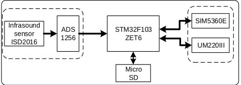
According to the function requirements, the data acquisition terminal of the debris flow monitoring system takes the STM32F103ZET6 as the core in the hardware design, and extends the ADS1256 analog-to-digital conversion, Micro SD card storage, 3G network communication module, GPS positioning module, W5500 Ethernet module, etc. The hardware structure block diagram is shown in Figure 2.
SIGNAL CONDITIONING CIRCUIT AND SAMPLING CIRCUIT
The core of the data acquisition terminal is a signal sampling circuit. In the sampling circuit, the data acquisition terminal uses the ISD2016 infrasound sensor developed by the Acoustics Institute of the Chinese Academy of Sciences to collect the infrasound signal of the debris flow. This sensor converts the infrasound wave collected into voltage signal with an amplitude not exceeding ±10V and transmits to A/D conversion module.
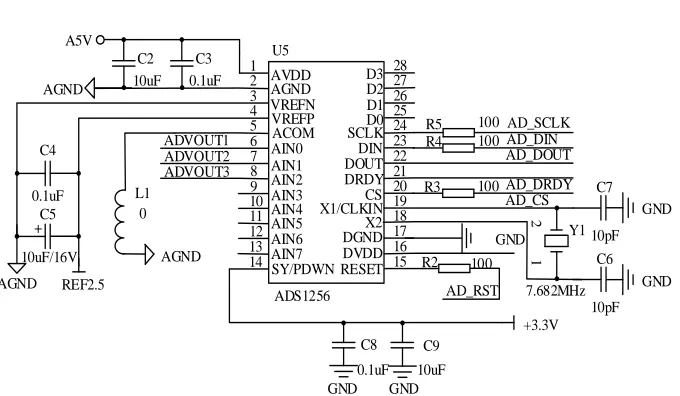
According to sampling rate and accuracy requirements, this paper selects the micro-power chip ADS1256 manufactured by TI company as the core of A/D conversion circuit. The programmable filter allows the user to optimize between a resolution of up to 23 bits noise-free and a data rate of up to 30k samples per second (SPS)[8-9]. In this design, the ADS1256 works in unipolar input mode. Its first three channels are used, and a crystal with the frequency of 7.682MHz to provide the clock signal.
[image:3.612.184.429.519.606.2]Since the ADS1256 can only input 0~5V voltage signals, it is necessary to convert the voltage signal whose amplitude is no more than ±10V to 0~5V voltage signal through the conditioning circuit. This design uses AD8275 from Analog Devices as the signal conditioning chip. With features of the low offset and low offset drift and the fast settling time, AD8275 is suitable for a variety of data acquisition applications where accurate and quick capture is required. Figure 3 shows the peripheral circuit of the AD8275.
Figure 2. The design diagram of hardware structure. STM32F103
ZET6
SIM5360E
UM220III ADS
1256 Infrasound
sensor ISD2016
REF1 -VS VIN-VIN+ REF2 SENSE +VS OUT C1 R1 1 2 3 4 8 7 6 5 4 1 3 2 P1 IN1 ADVIN1 U3 AD8275 VREF4096 ADVOUT1 1K 0.1uF A5V +15V -15V AGND
。
AGNDFigure 3. AD8275 peripheral circuit.
AVDD AGND VREFN R2 1 2 3 A5V
。
C2 10uF REF2.5 VREFP ACOM AIN0 4 5 6 AIN1 AIN2 AIN3 7 8 9 AIN4 AIN5 AIN6 10 11 12 AIN7 SY/PDWN 13 14 D3 D2 D1 28 27 26 D0 SCLK DIN 25 24 23 DOUT DRDY CS 22 21 20 X1/CLKIN X2 DGND 19 18 17 DVDD RESET 16 15 C3 0.1uF C5 10uF/16V C4 0.1uF R5 R4 AGND ADVOUT1 ADVOUT2 ADVOUT3 AGND L1 0 + AGND 100 100 AD_SCLK AD_DOUT AD_DIN AD_DRDY AD_CSR3 100 C7
10pF Y1 C6 10pF GND GND 2 1 GND 7.682MHz 100 AD_RST +3.3V C8 0.1uF C9 10uF GND GND ADS1256 U5
Figure 4. ADS1256 peripheral circuit.
The ±10V voltage signal output by the external sensor passes through the conditioning circuit to obtain a voltage signal of +0.048V~+4.048V, and after low-pass filtering, the voltage signal inputs the ADS1256 chip. The peripheral circuit of the ADS1256 is shown in Figure 4. ADS1256 adopts SPI bus as the data transmission mode to transmit the sampled data to the processor.
WIRELESS COMMUNICATION MODULE
[image:4.612.115.455.221.419.2]WIRED NETWORK PORT COMMUNICATION
The communication mode of the data acquisition terminal is mainly to send data to the monitoring terminal through the 3G wireless network. But in order to facilitate the on-site debugging of the staff, the data acquisition terminal of the design also has an additional wired network port communication interface. The design uses W5500 to read data from the data acquisition terminal. W5500, which has 8 independent hardware sockets simultaneously, enables users to have the Internet connectively in their applications just by using the single chip in which TCP/IP stack, 10/100 Ethernet MAC and PHY embedded. Without the need of an additional PHY chip, the W5500 just needs to install the RJ45 interface HR911105A which has a network transformer to start working. The network communication interface is shown in Figure 5.W5500 connects to MCU through SPI bus, which can keep a communication rate of 80 MHz
GPS SYNCHRONOUS CLOCK AND POSITIONING MODULE
The wireless data acquisition terminals mostly use three acquisition terminals to form a triangular array for data acquisition and they are mainly distributed in the field. Comparing with the three groups of data can get the final results. However, the delay of each collection terminal is inconsistent during the transmission process. Therefore, in order to obtain synchronous data, all data acquisition terminals need to use the same time standard [10]. Comparing with the 3G network timing, the design uses the domestic Beidou UM220IIIwhich has high sampling rate. GPS obtains the UTC time and corrects error by second pulse, getting the final system time whose relative error is less than 20ns.
THE SOFTWARE DESIGN OF DATA ACQUISITION TERMINAL
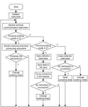
The workflow of the data acquisition terminal is shown in Figure 6. After power on, the system initializes the clock, serial port, interrupt, and data acquisition terminal modules. After the initialization is completed, the data acquisition terminal, according to the status of system network connection and the need of monitoring terminal, enters different working mode separately by the control command of communication protocol.
accumulate, the system will automatically save data instruction packet to the SD card in time. Meanwhile, the data acquisition terminal continuously detects the network interface and attempts to connect to the network. The system cycles in this modeto wait for new connection.
STM32 W5500 HR911105A
RST RST
INT MOSI
MISO
SCLK
/CS
INT MOSI
MISO
SCLK
/CS
TXD
TXN RXN
RXP
ACTLED
LINKED
TD+
TD-RD+
RD-GRN+
YEL-Figure 5. W5500 interface connection diagram.
Start
Initialize subroutine
Terminal working mode is 1?
Complete the instructions?
Change working mode
Terminal working mode is 2?
Data collection subroutine
Save data to SD card Y
N
Y N
Y
Y
Y N
N Monitor terminal
communication subroutine
Monitor terminal instruction processing subroutine
Try to connect to a 3G network
3G connection is successful?
Change working mode
Data collection subroutine
3G connection is successful?
Change working mode Send
sampling data
[image:6.612.173.419.164.265.2]N
[image:6.612.155.449.300.656.2]A/D Sampling Subroutine
When the data acquisition terminal has obtained the running time of the system and the staff have started up the device, the terminal begins A/D sampling by the internal timer whose unit isμs. This design selects ADS1256 as the core of the data conversion circuit, and its sampling accuracy is 24 bits. The initialization of the ADS1256 chip will set 2000SPS sample output, so that its own sampling rate of up to 30KSPS is used for oversampling. And the average value is taken by multiple samples to improve the accuracy of the sampled data.
Different sampling frequencies are achieved by setting the sampling interval. The system enters the A/D sampling subroutine when the set sampling time is up.
Network Port Communication Subroutine
When the staff is debugging on the spot, the computer sending control command to the data acquisition terminal through the network port will trigger interrupt. The data acquisition system platform can provide the selection of system parameters, channels and sampling rates, the display of real-time data, and the reading, querying, playback, and export of historical data. It can also send different control command through the network port to set the working state of the device.
SYSTEM TEST
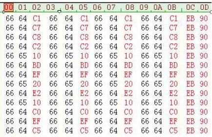
The system was tested in Dashu Town, Fengjie County, and Chongqing. Figure 7is the on-site debugging diagram. Figure 8 shows a screenshot of part test data stored by the monitoring terminal while the input voltage is 4V. Every six-digit hexadecimal number represents a sampling voltage value. The channel samples input data continuously for 4 times to indicate that the work is normal and stable.
The voltage value stored in the monitoring terminal can be obtained from Equation 1:
23
2
D (2 1)
REF
V PGA
(1)
D is the decimal number coded for monitoring terminal storage. VREFis the 2.5V
reference voltage. PGA is the gain multiple of 1. The number 6664EF equals to the decimal number 6710511, 2 2.5/ (223-1) 6710511=3.9997767;The number
6664C8 equals to the decimal number 6710472, 2 2.5/ (223-1)
Figure 7. On-site debugging chart.
Figure 8. Diagram of part test data.
CONCLUSIONS
[image:8.612.198.415.262.402.2]REFERENCES
1. Z. Chen, R. Deng, and Z. Song. 2016. “Analysis of the Formation Mechanism and Blockage of Zhuzha Gully Debris Flow Disaster in Shimian of Sichuan on July 4th, 2013,” The Chinese Journal of Geological Hazard and Control, 27(3):42-46.
2. C. Ouyang, S. He, and C. Tang.2015. “Numerical Analysis of Dynamics of Debris Flow over Erodible Beds in Wenchuan Earthquake-Induced Area,” Engineering Geology, 194:62-72. 3. C. Li, L. Wang, and K. Liao. 2014. “Study of Early Warning Mechanism of Debris Flow along
Railway Lane in Mountainous Areas,” Chinese Journal of Rock Mechanics and Engineering,33(2): 3811-3816.
4. J. Tu, Y. Yang, C. Li, A. He, and L. Li. 2015. “A Context-Adaptive and Energy-Efficient Wireless Sensor Network for Debris flow Monitoring,”2014 International Conference on Wireless Communication and Sensor Network. 157-162.
5. J. Chiu, C. Dow, C. Lin, J. Lin, and H. Hsieh. 2012. “A Watershed-Based Debris Flow early Warning System Using Sensor Web Enabling Techniques in Heterogeneous Environments,” IEEE Journal of Selected Topics in Applied Earth Observations and Remote Sensing. 5(6):1729– 1739.
6. K. H. Xu, D. Zhang, and Y. H. Liu. 2013. “Design of Deformation Monitoring Terminal System Based on STM32,” Applied Mechanics and Materials, Vols. 347-350, pp. 628-633.
7. Z. Shi, P. Zhang, and A. Shu. 2010. “Forecast and early Warning System for Debris Flow Monitoring,” Journal of Yangtze River Scientific Research Institute, 27(11): 116-119.
8. Y. Su, J. Cao, and L. Cheng. 2016. “Application of ADS1256 in High Precision Data Acquisition System,” Electronic Science & Technology, 3(5):546-548.
9. M. Zhang, Z. Xiao, and Y. Yang. 2013. “Seismic Data Acquisition Circuit Design. Modern Electronics Technique,” 36(24):134-135, 139.