2018 International Conference on Applied Mechanics, Mathematics, Modeling and Simulation (AMMMS 2018) ISBN: 978-1-60595-589-6
Design of Control System for Dynamic Calibration Device of Eddy
Current Sensor Based on FPGA
Xiao HE, Xiang XU* and Sen YANG
Hongta Tobacco (Group) Co., Ltd., Yuxi653100, China
*Corresponding author
Keywords: Eddy current sensor, Dynamic calibration, Automation, FPGA.
Abstract. In the dissertation, an automatic and integrated calibration device for the static characteristics of eddy current sensors was researched aimed at the great demand of improving the efficiency of calibrating eddy current sensors. The design proposal for the control system in the slave computer of automatic and integrated calibration device for the dynamic characteristics of eddy current sensors was studied. The control method of vibration level automatic adjustment was proposed. A signal generator, a data acquisition unit and a data storage unit were designed. Besides, the serial communication module was also designed to communicate with the master computer.
Introduction
The dynamic calibration of the eddy current sensor is mainly realized through vibration calibration. At present, the main way to complete the vibration calibration is to use the dynamic calibrator or standard vibration table. The former, such as herat instrument electronics co., LTD., has designed a dynamic calibration device of the electric eddy current sensor with a rotating inclined plate. This device can drive the periodic rotation of the inclined induction plate through the motor, and change the distance between the electric eddy current sensor and the induction plate to simulate the vibration. However, the device structure is simple, but the calibration frequency range is limited[1-2]. At the same time, there is an Angle between the sensor plate and the calibrated sensor, which will introduce the calibration error. The calibration method of the latter is developed with the development of vibration measurement technology in China[3-4]. In this paper, the design of the control system of the standard vibration table is studied.
Scheme Design
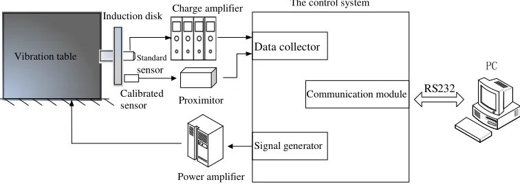
[image:1.612.111.489.570.704.2]Design of dynamic calibration control system of electrical vortex sensor mainly includes design of control technology of level of vibration standard exciter, and sine signal generating module with frequency and amplitude adjustable, design of data collection module and design of serial port communication module communicating with principal computer.
Figure 1. Structure of dynamic calibration system of electrical vortex sensor.
Standard
sensor
Calibrated sensor Induction disk
Power amplifier
Signal generator Proximitor
Charge amplifier
Vibration table
RS232 Data collector
The control system
PC
The device realizes dynamic calibration of electrical vortex sensor with comparison method, the standard acceleration suite adopts international 3506 suite of B&K Company, including standard acceleration meter 8305 and charge amplifier 2525, and the structure of dynamic calibration of electrical vortex sensor is as shown in Figure 1.
Sinusoidal Signal Generating Module
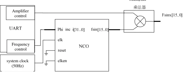
In dynamic calibration of electrical vortex sensor, a signal which can drive sense element to take standard sinusoidal vibration, NCO (digital vibrator) IP core at the embedded function unit of bottom of FPGA can achieve this function conveniently[5-7].
[image:2.612.103.497.208.300.2]The principle of NCOIP based on ROM is as shown in Figure2.
Figure 2. Work principle of NCO IP core based on ROM.
The NCO IP core is called in the Megawizard Plug-In Manager of the FPGA development software Quartus II. The frequency control word and the amplitude control word are assigned to the NCO IP core and multiplier respectively through the serial communication module, and the system clock is used as the NCO working clock. The structure block diagram of sinusoidal signal generator is shown in Figure 3.
Figure 3. Structure block diagram of sinusoidal signal generator.
In order to verify whether the module can work normally, functional simulation can be carried out. This design adopts modelsim tool of QuartusII to achieve stimulation, prepare test bench test document, put drive signal to input pin to complete stimulation of NCO function, the stimulation results are as shown in Figure 4.12, NCO digital oscillator produces sinusoidal signal with difference frequency and amplitude with change of frequency and amplitude index, which indicates that NCO can complete the function.
Frequency
control Accumulator Phase register Adder
Phase control
sampling clock
Look-up table Output Sin/cos output register
Frequency control Amplifier
control
Multiplier
[image:2.612.154.459.422.544.2]Figure 4. Stimulation waveform of NCO function.
Data Collection Module
In dynamic calibration of electrical vortex sensor, it is required to collect the output signal of the calibrated electrical vortex sensor. So it is necessary to design a sensor output signal collection module. Considering no distortion in sampling of sensor output signal in the process of dynamic calibration, higher data collection rate is needed, therefore, 24-bit data collection chip with sampling rate of 100kSPSADS1271 is chosen[8].
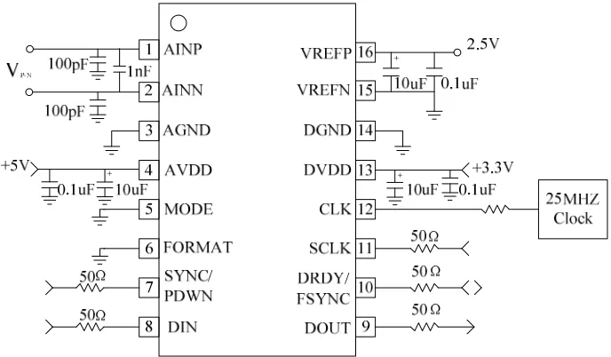
Design of Power Supply Circuit
Design of ADS1271 circuit involves design of power supply, input signal conditioning circuit, the electrical principle is as shown in Figure 5.
Figure 5. Electrical principle of ADS1271 in working.
When using ADS1271, 5V stimulation power supply, 3.3V digital power supply and 2.5V reference voltage source should be provided from outside, the reference voltage is stimulation voltage of 5V, which is obtained by REF2125, other power supplies are obtained from 220V AC transformer through rectification, filtration and voltage stabilization.
Input of Stimulation Signal
[image:3.612.147.491.378.579.2]signal of VREF(2.5V), and the range of signal input of sensor is 24V, so the output signal of sensor must be accepted by ADS1271 after conversion, mode of conversion is selected to ensure high input resistance of output signal of sensor, no distortion of input signal, so two-level low noise high-voltage operational amplifier is designed[9]. Principle diagram of conditioning circuit of input signal of ADS1271 is as shown in Figure 6.
Figure 6. Principle diagram of input signal conditioning circuit.
Stimulation Verification of ADS1271 Control Program
[image:4.612.107.507.425.501.2]This design adopts Modelsim tool to stimulate, prepare test bench test code to stimulate ADS1271 timing sequence. Figure 7 shows control program stimulation waveform of ADS1271, DRDY signal with frequency of 100KHz is provided for input interface in the stimulation, test_data is the test data, DATAIN is series input signal, dataout is output of data collected by ADS1271. The results indicate that the data collected by ADS1271 is consistent with test data, certifies the correctness of program logic functionality.
Figure 7. Stimulation waveform of ADS1271 control program.
Communication Module
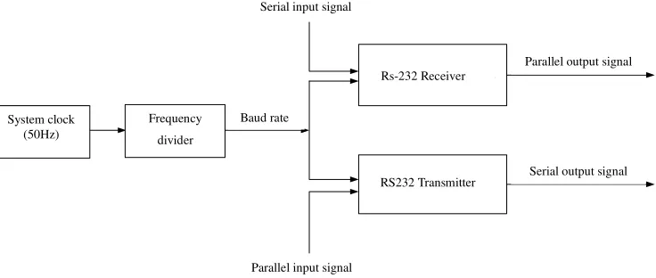
In design of automatic calibration device of dynamic characteristic of electrical vortex sensor, the function to be completed by communication module is to realize normal signal transfer between principal computer and slave computer. The Baud rate of device is 9600bit/s. RS232 standard serial port is to achieve data sending and receiving with 8 data bits as a unit, and the frame format of sending and receiving interface is as shown in Figure 8.
Figure 8. Frame format of serial port communication sending and receiving interface.
Design of serial port communication module is realized with VHDL language, including design of Baud rate generator, data receiver and data transmitter, and the serial input and parallel output are
± ±
[image:4.612.135.484.638.682.2]achieved by data receiver. The data transmitter achieves the parallel input and serial output of data [10]
[image:5.612.114.482.111.267.2]. The realization structure of communication module is shown in Figure 9.
Figure 9. Schematic diagram of structure of realization of serial port communication.
In order to verify the correctness of design of serial port communication program, the data receiver and transmitter of the communication module are simulated with Modelsim tool of Quartus II. The simulation results are as follows.
[image:5.612.91.519.556.630.2]Figure 10 shows the simulation of the data receiving module, sys_clk means the clock input signal, which receives the clock output signal from the Baud rate generator; rxd means the serial communication data receiving port, and the signal is inputted from this port; dout means the parallel output port; rcv_count means the counter of number of the received signals; read_flag means the cpu read ready signal. rxd is assigned with a certain value as the serial input of the receiving module. The serial data is output to the parallel output port dout through shift register. According to the communication protocol of the calibration system, the serial input includes 96-bit data. The frame format of serial port communication receiving and sending interface needs to have start bit, check bit, stop bit and idle bit, each 8-bit data of frame format of serial port communication receiving and sending interface need to have start bit, check bit, stop bit and idle bit, 8-bit data shift in the program needs to achieved through counting of rcv_count for 12 times, so when completing shift of 96-bit data, rcv_count reaches 144, at this point, cpu reads ready signal, read_flag rises to high level, which indicates that cpu is ready to read signal, the shift register outputs the received valid data, and dout displays the received data. As shown in Figure 4.36, the simulation results are consistent with the program design, which indicates that the data receiving module works normally.
Figure 10. Simulation diagram of serial port communication data receiving module.
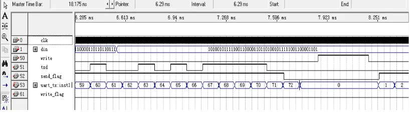
Figure 11 is the simulation diagram of data sending module, in the figure, sys_clk means clock input interface, din means 48-bit parallel input interface, and send_flag means data shift transmission signal. txd means uart serial data sending port, write means to write indicating signal by CPU, and send_count means counter of number of the transmitted data. In simulation, the din is assigned a certain value as the parallel input of the receiving module. When the write signal is high, the parallel data is output from the shift register to the serial output interface txd, similarly, for
System clock (50Hz)
Frequency divider
Baud rate
Serial input signal
Parallel input signal
Rs-232 Receiver
RS232 Transmitter
Parallel output signal
48-bit data, each shift of 8-bit data requires 12 times of counting of send_count, so when 48-bit of data are shifted, send_count reaches 72, and the data shift transmission signal send_flag is raised to high level. Data are exported serially from txd. As shown in Figure 11, the simulation results are consistent with the program design, which indicates that the data receiving module works normally.
Figure 11. Simulation diagram of serial port communication data sending module.
Summary
In the design of the control system of the automatic calibration device for the dynamic characteristics of the eddy current sensor, the design of signal generator was completed by QuartusII. The data collector and Communication module was also completed by the use of ADS1271 and RS232 Respectively. The correctness was verified by Stimulation.
Reference
Pan Liangming. Development and research of vibration calibration device measurement and control system [D]. ZheJiang University, 2006, 54-58.
Wang Zhipeng. Research on automatic measurement and control system of ultra-low frequency vibration calibration device [D]. ZheJiang University, 2011, 35-40.
Li Gen. Study on automatic calibration system of digital display vibration meter [D]. ZheJiang University, 2012, 67-69
Wang Chunyu. Research on design theory and motion control technology of ultra-low frequency standard vibration table [D]. ZheJiang University, 2013, 13-15
Li Dadu. Design example elaboration of FPGA/CPLD based on Quartus II [M]. Beijing: Publishing House of Electronics Industry, 2012, 154-156.
Chen Shao-kuan, Li Ming. Research and FPGA Implement of NCO [J]. Instrumentation Technology. 2006(05), 30-32.
Liu Huadong. Altera series FPGA chip IP core details [M].BeiJing: Publishing House of Electronics Industry, 2014, 265-266.
Li Linghua, He Lijun. Principle and Application of the 24 - bit, Wide Bandwidth, Delta - sigma Analog - to - Digital Converter ADS1271 [J]. Modern Electronics Technique, 2007 (16).4-6, 12.
Zhang Yunchang. Research and implementation of multi-channel dynamic data acquisition system [D]. Nanjing University of Aeronautics and Astronautics, 2008, 23-24.