FPGA Message Passing
Cluster Architectures
by
Eoin Creedon, B.A. (Mod.) Computer Science
Thesis Presented to the University of Dublin, Trinity College in fulfilment of the requirements for the degree of
Doctor of Philosophy (Computer Science)
Declaration
I, the undersigned, declare that this work has not been previously submitted to this or any other University, and that unless otherwise stated, it is entirely my own work.
Permission to Lend and/or Copy
I, the undersigned, agree that Trinity College Library may lend or copy this thesis upon request.
A
BSTRACT
This work investigates inter-Field Programmable Gate Array (FPGA) communication mechanisms, specifically the use of message passing and switched Ethernet communication mechanisms. Inter-FPGA communication is required in situations where the computational demands of an algorithm cannot be satisfied by a single FPGA. To meet the algorithms requirements, it must be implemented over several FPGAs. This leads to the need for remote register transfer operations that allow for the exchange of data and synchronisa-tion between aspects of the algorithm that are implemented on each individual FPGAs. The algorithm is de-fined using a Hardware Description Language allowing it to be implemented through the reconfigurable logic of the FPGA. This thesis argues for an implementation of the data exchange and synchronisation mecha-nisms that facilitate remote register transfer operations in reconfigurable logic on the FPGA. This approach allows for a definition in Hardware Description Language and therefore can provide the application pro-grammer with a Hardware Description Language Application Programming Interface that is simple to inte-grate into the application and hides the implementation of the communication mechanisms from the applica-tion programmer. A message passing protocol is used to implement the remote register transfer operaapplica-tions.
Message passing and switched Ethernet are argued for as the approach to be taken as they support algorithm parallelisation in a scalable and robust manner. Using the Hardware Description Language Mes-sage Passing Application Programming Interface (HDL MP API) facilitates both the remote register transfer operations between FPGAs and also between FPGAs and workstations. The message passing and switched Ethernet operations can be implemented using either a dedicated hardware microarchitecture or an FPGA processor, with the HDL MP API developed to abstract the application from which data exchange approach is being taken. By looking at both approaches, this thesis argues for the feasibility of message passing in conjunction with switched Ethernet as a viable platform for supporting application parallelisation across in-terconnected FPGAs. To support this, discussions on characteristics of various parallel algorithms aid in demonstrated which approach is suitable for a given set of algorithm requirements.
A
CKNOWLEDGEMENTS
The work in this thesis is the culmination of a number of years of research. Firstly, I would like to thank my supervisor Dr. Michael Manzke for his assistance throughout this research. His guidance helped refine many different aspects of the research that was undertaken. I would also like to thank Ross Brennan, Muiris Woulfe, Owen Callanan, Milan Tichy, Jeremy Jones and David Gregg for their assistance at different times. I would like to thank my examiners, Peter Cheung and Stefan Weber, for an interesting and insightful viva.
The technologies used within this thesis, in particular Ethernet, required an amount of technical ex-pertise to help identify and resolve various issues that presented themselves in this work. For assistance at different times on finding solutions to these, I would like to thank Martin McCarrick, Mark Gleeson and the technicians within the Department of Computer Science. Thanks are also due to James Wright for assistance in acquiring some of the Xilinx development boards that have been used within a range of experiments.
I would like to thank all my friends who assisted me with the work at different stages, Dervla O’Keeffe, David Humphreys, Brian Kelly and Colm Moore. I would also like to thank friends that I have made over the years of my Ph.D. including Aoife Foley, Ruth Canavan and everyone else from the GSU that I have come to know.
i
T
ABLE OF
C
ONTENTS
Table of Contents ... i
List of Figures ... iii
List of Tables ... vii
List of Acronyms... ix
Chapter 1 Introduction ... 1
1.1 Research Statement... 6
1.2 Thesis Structure and Layout ... 10
Chapter 2 Background and Related Work ... 13
2.1 Parallel Algorithms ... 14
2.2 Parallel Programming on Microcomputers ... 18
2.3 FPGA Algorithms and Acceleration ... 33
2.4 Interconnected FPGA Architectures ... 43
2.5 Algorithms over Multiple FPGAs... 50
2.6 FPGA Message Passing ... 55
2.7 Related Work ... 57
2.8 Summary and Motivation ... 68
Chapter 3 Design ... 71
3.1 Message Passing ... 73
3.2 Interconnect Communication Operations ... 83
3.3 Algorithm Data Interface ... 92
3.4 Management Node... 93
3.5 HDL MP API Evaluation Design ... 93
3.6 Algorithm Design Considerations... 99
3.7 Summary... 99
Chapter 4 Implementation ... 101
4.1 Common Implementation Features... 102
4.2 Hardware Microarchitecture Implementation ... 120
4.3 Software FPGA Processor Implementation ... 133
4.4 Management Node... 140
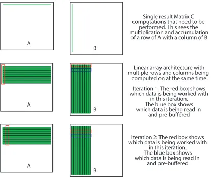
4.5 Matrix Multiplication Architecture... 142
4.6 Memory System Interface Development ... 146
Chapter 5 Evaluation ... 155
5.1 Stress Test Experiments... 156
5.2 Benchmark Experiments... 163
5.3 Collective and Scalability Experiments ... 185
5.4 Parallel Matrix Multiplication ... 192
5.6 Evaluation Conclusions ... 231
Chapter 6 Conclusions and Future Work ... 235
6.1 Limitations... 237
6.2 Future Work... 239
Appendix A FPGAs ... 241
A.1 Compute Resources ... 241
A.2 FPGA Processors ... 241
A.3 Memory Technologies ... 242
A.4 Clock Management... 243
A.5 FPGA On-Chip Interconnection Strategies ... 245
A.6 Commodity FPGA Accelerator Architectures ... 248
Appendix B Interconnection Technologies ... 251
B.1 Internode Connection Networks ... 251
Appendix C Node Synchronisation ... 253
iii
L
IST OF
F
IGURES
Figure 1: On-FPGA register transfers ... 3
Figure 2: Multiple interconnected FPGA application microarchitectures ... 4
Figure 3: Parallel Algorithm Mapping Overview ... 7
Figure 4: Microarchitecture acceleration structure ... 34
Figure 5: Systolic Array acceleration structure... 34
Figure 6: Multi-FPGA Architecture... 44
Figure 7: Distributed FPGA Architecture ... 44
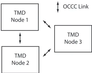
Figure 8: TMD Architecture ... 58
Figure 9: OCCC Link Structure... 59
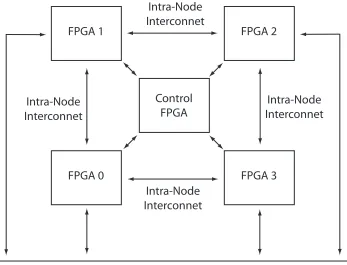
Figure 10: BEE2, RAMP node configuration ... 65
Figure 11: Architectural operation design ... 71
Figure 12: Message Passing Send Design... 76
Figure 13: Message Passing Receive Design... 77
Figure 14: Message Passing Send/Receive Protocol Operations ... 78
Figure 15: Message Passing Communication Initialisation ... 79
Figure 16: Initialisation Flow Control Operations ... 80
Figure 17: Design flow for unit identity conversion ... 80
Figure 18: Receive Flow Operations ... 86
Figure 19: Transmit Flow Operations... 87
Figure 20: Message Passing Communication Flow Layout... 88
Figure 21: Padded Algorithm Comparison example... 91
Figure 22: Non-Padded Algorithm Comparison example... 92
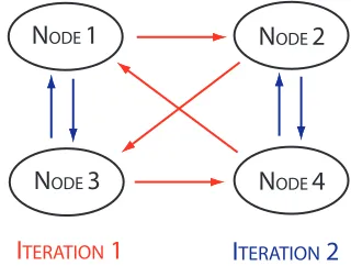
Figure 23: Compute unit computation ordering... 97
Figure 24: Ring topology layout ... 98
Figure 25: Matrix Computation Ordering ... 98
Figure 26: 3 Node Barrier Communication Pattern ... 107
Figure 27: 4 Node Barrier Communication Pattern ... 107
Figure 28: MPICH, broadcast communication structure ... 108
Figure 29: FPGA stream pipeline broadcast communication structure ... 108
Figure 30: FPGA Scatter Operation... 109
Figure 31: FPGA Gather Configuration... 109
Figure 32: AllGather Communication Topology ... 110
Figure 33: AllToAll Communication Topology ... 110
Figure 34: Communication Operation Structure... 112
Figure 35: MAC Update Configuration ... 114
Figure 36: Non Back-to-Back Packets... 117
Figure 38: Hardware and Software Configuration Layout... 120
Figure 39: Communication Control Configuration ... 121
Figure 40: Hardware Message Passing Architectural Configuration ... 122
Figure 41: Initialisation Algorithm Operations... 123
Figure 42: Transmit Message Queue ... 125
Figure 43: Receive Message Queue... 125
Figure 44: Hardware Control Logic Configuration... 127
Figure 45: Crossbar Interconnect Structure ... 128
Figure 46: Receive Packet Control ... 130
Figure 47: Transmit Flow Control ... 131
Figure 48: Hardware System Architecture... 133
Figure 49: Software FPGA Processor Architecture ... 137
Figure 50: Message Passing Implementation Architectures ... 140
Figure 51: Base Processing Element Structure ... 143
Figure 52: Linear Array Configuration ... 146
Figure 53: Memory Interface Developmental Configurations ... 147
Figure 54: Measured Memory Bandwidth ... 154
Figure 55: Packet Drop Rate... 158
Figure 56: FS108 Latency performance ... 167
Figure 57: FS508 Latency performance ... 167
Figure 58: Cisco Latency performance... 168
Figure 59: GS608 Gigabit Latency performance ... 168
Figure 60: Crossover latency performance ... 169
Figure 61: Hardware 100Mb Message Passing Exchange ... 175
Figure 62: Software 100Mb Message Passing Exchange ... 176
Figure 63: Hardware 1000Mb Message Passing Exchange ... 176
Figure 64: Software 1000Mb Message Passing Exchange ... 177
Figure 65: FS108 Bandwidth ... 180
Figure 66: FS508 Bandwidth ... 180
Figure 67: Cisco Bandwidth ... 181
Figure 68: GS608 Bandwidth ... 181
Figure 69: Network Bandwidth, Consistent DDR Memory... 183
Figure 70: Network Bandwidth, Coherent DDR Memory... 183
Figure 71: Initialisation Timings ... 187
Figure 72: Barrier Synchronisation Times... 189
Figure 73: Scaling Experiment, per node best performance ... 198
Figure 74: Matrix Multiplication Performance Breakdown, 1 Node ... 199
Figure 75: Matrix Multiplication Performance Breakdown, 2 Nodes ... 200
Figure 76: Matrix Multiplication Performance Breakdown, 3 Nodes ... 200
v
Figure 78: Speed-up graph for various sizes... 202
Figure 79: Measured Application Network Bandwidth ... 203
Figure 80: Scaling Experiment, Burst, per node performance ... 205
Figure 81: Matrix Multiplication Performance Breakdown, Burst, 1 Node... 206
Figure 82: Matrix Multiplication Performance Breakdown, Burst, 2 Nodes ... 206
Figure 83: Matrix Multiplication Performance Breakdown, Burst, 3 Nodes ... 207
Figure 84: Matrix Multiplication Performance Breakdown, Burst, 4 Nodes ... 207
Figure 85: Parallel Matrix Multiplication Times, Burst... 208
Figure 86: Burst speedup graph for various sizes ... 209
Figure 87: Measured Application Network Bandwidth, Burst ... 210
Figure 88: Moloch Scaling Matrix Performance Figures... 211
Figure 89: Moloch Parallel Computation time... 212
Figure 90: Matrix Multiplication, Cyclic Test Performance Results ... 213
Figure 91: Fragmentation FPGA Hardware results, 100Mb ... 220
Figure 92: Fragmentation FPGA Software results, 100Mb ... 221
Figure 93: Fragmentation FPGA Hardware results, Gigabit... 221
Figure 94: Fragmentation FPGA Software results, Gigabit ... 222
Figure 95: PC experiment results for 100Mb Ethernet ... 223
Figure 96: PC experiment results for Gigabit Ethernet... 223
Figure 97: TCP/IP Fragmentation experiment, live 100Mb network ... 226
Figure 98: TCP/IP Fragmentation experiments, closed 100Mb network... 227
Figure 99: TCP/IP Fragmentation experiments, closed Gigabit network ... 227
Figure 100: TCP/IP Fragmentation experiments, closed Gigabit network, MTU 5000... 228
Figure 101: TCP/IP Fragmentation experiments, closed Gigabit network, MTU 7000... 229
Figure 102: TCP/IP Fragmentation experiments, closed Gigabit network, MTU 9000... 229
vii
L
IST OF
T
ABLES
Table 1: HDL MP API Communication Commands ... 75
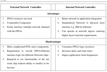
Table 2: Network Controller Design Location Considerations... 90
Table 3: Interconnection Communication Sizes ... 90
Table 4: Classical Matrix Multiplication Algorithm... 95
Table 5: Linear Array Matrix Multiplication Algorithm ... 96
Table 6: Sample Verilog Communication interface code ... 103
Table 7: HDL MP API Communication interface signals ... 105
Table 8: HDL MP API Memory interface signals ... 152
Table 9: AMBA DDR Memory Bandwidth... 153
Table 10: Stability Experiment Resource Utilisation... 157
Table 11: Stability Test Results, Cisco Catalyst 3548 XL... 159
Table 12: Stability Test Results, Netgear FS108 ... 160
Table 13: Stability Test Results, Netgear FS508 ... 160
Table 14: Stability Test Results, Netgear GS608... 161
Table 15: Latency Experiment communication components ... 165
Table 16: Latency Experiment Resource Utilisation ... 165
Table 17: FPGA Message Passing Latency (µs)... 170
Table 18: PC Latency MPI Communication (µs)... 171
Table 19: Message Passing Experiment Resource Utilisation ... 173
Table 20: Block RAM exchange time... 174
Table 21: Bandwidth Experiment Resource Utilisation... 179
Table 22: Maximum Network Bandwidth ... 182
Table 23: Initialisation Experiment Resource Utilisation ... 186
Table 24: Hardware Collective Operations Logic Footprint... 190
Table 25: Software Collective Operations Logic Footprint ... 191
Table 26: Matrix Multiplication, Classical configuration ... 194
Table 27: Linear Array, Parallel Matrix Multiplication Experiment Resource Utilisation... 197
Table 28: Linear Array, Parallel Matrix Multiplication Burst Experiment Resource Utilisation ... 204
Table 29: Additional Node Performance Boost, Scaling ... 205
Table 30: Additional Node Performance Boost, Parallel... 208
Table 31: Fragmentation Experiment Resource Utilisation ... 219
Table 32: Bus Interconnection, 3 masters, 3 slaves – FF896 ... 256
Table 33: Crossbar Interconnection, 3 masters, 3 slaves – FF896 ... 256
ix
L
IST OF
A
CRONYMS
AAL Acceleration Abstraction Layer ACC Adaptable Compute Cluster ADI Abstract Device Interface
AHB Advanced High-performance Bus
AMBA Advanced Microcontroller Bus Architecture APB Advanced Peripheral Bus
API Application Programming Interface ARP Address Resolution Protocol
ASIC Application Specific Integrated Circuit BD Buffer Descriptor
BEE2 Berkley Emulation Engine 2 BT Block Tridiagonal Solver CFD Computational Fluid Dynamic CG Conjugate Gradient
CMP Chip MultiProcessor CNP Compute Node Platform CRC Cyclic Redundancy Check CTS Clear To Send
CUDA Common Unified Device Architecture DCM Digital Clock Management
DDR Dual Data Rate
DIMM Dual Inline Memory Module DMA Direct Memory Access
DRMC Distributed Reconfigurable Metacomputer DSM Distributed Shared Memory
EDK Embedded Development Kit
EEPROM Electrically Erasable Programmable Read-Only Memory EMP Ethernet Message Passing
eMPI Embedded MPI EP Embarrisingly Parallel
FEMPI Fault-tolerant Embedded MPI FFT Fast Fourier Transform
FHPCA Field Programmable High Performance Computer Architecture FIFO First In, First Out
FSB Front Side Bus
FT 3D FFT Partial Differential Equations GASNet Global Address Space Network GCN Graphics Cluster Node
GFLOPS Gigabyte Floating-Point Operations per Second GFLOPS Gigabyte Floating-Point Operations Per Second GMII Gigabit Media Independent Interface
GPU Graphics Processing Unit HDL Hardware Description Language
HDL MP API Hardware Description Language Message Passing Application Programming Interface HDLC High-level Data Link Control
HPC High Performance Computing I/O Input/Output
IBM International Business Machine
IEEE Institute of Electrical and Electronics Engineers ILP Instruction Level Parallelism
INIC Intelligent Network Interface Controller IP Internet Protocol
IPSec Internet Protocol Security IS Integer Sort
iWARP Internet Wide Area RDMA Protocol JNIC Joint Network Interface Controller LA Los Alamos
LAM Local Area Multicomputer LED Light Emitting Diode LMB Local Memory Bus LMPI Lightweight MPI LRU Least Recently Used LU LU Solver
LUT Look Up Table
MAC Media Access Controller MD Molecular Dynamic
MFLOPS Megabyte Floating-Point Operations Per Second MG Multigrid
MGT Multi-Gigabit Transceiver MII Media Independent Interface
MIPS Millions of Instructions Per Second MPI Message Passing Interface
xi NAS Numerical Aerodynamic Simulation
NIC Network Interface Controller NoC Network-on-Chip
NPB NAS Parallel Benchmark NUMA Non-Uniform Memory Access OCCC Off Chip Communication Core OPB On-Chip Peripheral Bus
OS Operating System
OSI Open Systems Interconnect PC Personal Computer
PCB Printed Circuit Board
PCI Peripheral Component Interconnect PLB Processor Local Bus
PUMMA Parallel Universal Matrix Multiplication Algorithms PVM Parallel Virtual Machine
QCD Quantum Chromo Dynamics QDR Quad Data Rate
RAM Random Access Memory
RAMP Research Accelerator for Multiple Processors RASC Reconfigurable Application Specific Computing RASCAL RASC Abstraction Layer
RCC Reconfigurable Compute Cluster RDMA Remote Direct Memory Access RISC Reduced Instruction Set Computer ROM Read Only Memory
RTS Request To Send
RWCP Real World Computing Partnership
SAMRAI Structured Adaptive Mesh Refinement Application Infrastructure SAN System Area Network
SATA Serial Advanced Technology Attachment SCE SMILE Communication Element
SDR Single Data Rate
SDRAM Synchronous Dynamic Random Access Memory SGI Silicon Graphics Inc.
SIMD Single Instruction, Multiple Data SMP Symmetric Multi-Processor SoC System-on-Chip
SRAM Static Random Access Memory SUE Spin Update Engine
TCHPC Trinity Centre for High Performance Computing TCP Transmission Control Protocol
TCP/IP Transmission Control Protocol/Internet Protocol
TMD-MPI Toronto Molecular Dynamics-Message Passing Interface UCF User Constraint File
UDP User Datagram Protocol UMA Uniform Memory Access UPC Unified Parallel C
1 of 257
Chapter 1
Introduction
Raw computational performance of computer processors continues to increase, in terms of Millions of Instructions Per Second (MIPS), Floating-Point Operations per Second (FLOPS) and in the number of opera-tions that can be processed concurrently through the use of Single Instruction, Multiple Data (SIMD) Exten-sions, Multi-Core architectures and Instruction Level Parallelism (ILP). However, even as microprocessor performance increases, through the use of these techniques, they are still unable to meet the computational requirements of certain algorithms, mainly scientific e.g. Lattice Quantum Chromo Dynamics (QCD). To meet the computational requirements of these algorithms, further parallelism is required with computations typically spread across a number of computation elements with a data exchange and synchronisation mecha-nism employed to ensure all computations are performed correctly and in the correct order.
To support the development of algorithms running on the various architectures, special program-ming approaches are used. For cluster solutions, this has seen the development of parallel programprogram-ming ap-proaches which allow the different computation resources to operate on different aspects of an algorithm in parallel. The parallel programming approaches support the exchange of data between the computation ele-ments, ensuring all algorithm computations are performed. The notion of parallel programming and by ex-tension, parallel computation, corresponds to multiple computation units performing distinct computations of an algorithm at the same time on different computation resources. Parallel programming is the use of specific programming approaches which support parallel computations through the provision of synchronisation and data exchange mechanisms between the computation units. This thesis focuses on the use of parallel pro-gramming techniques as they pertain to interconnected FPGAs which are able to operate independently of a computer system. The use of directly interconnected FPGAs is a refinement of the compute cluster and co-processor approach with the computer removed and the FPGAs performing all communication and computa-tion operacomputa-tions, as peers of each other, independently of a controlling computer.
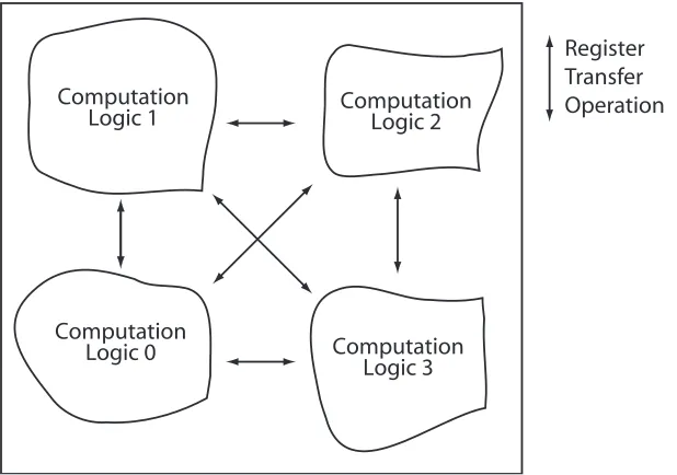
An FPGA is a reconfigurable hardware device where an algorithm can be implemented to use the hardware resources in a manner best suited to that algorithm. The algorithm is implemented using a Hardware Description Language (HDL) which allows the programmer to define the physical hardware and how data is exchanged between different compute units on the FPGA. This allows the algorithm to be highly parallelised on a single FPGA. The exchange of data between computation resources on an FPGA is typi-cally done using a register transfer operations. Register transfer sees the exchange of data from one compute unit to another where the data will be required for future computations. An overview of this type of opera-tion and data exchange is shown in Figure 1. Here, the distinct computaopera-tion units of an algorithm operate on their data but use register transfer to exchange data with other computation logic that will require it. Each compute unit can be viewed as a specific computation microarchitecture which performs a specific aspect of the larger algorithm. The use of the register transfer model is practical when a single FPGA is large enough to support all algorithm computations. As an FPGA is a hardware device however, there is a limit to the amount of resources that are available. Once the resources of a single FPGA have been exhausted, no addi-tional computations can be performed. Like the computer processor before it, a means to increase the avail-able computation resources needs to be found which will support the increased requirements of an algorithm. A practical means to achieve this is to use multiple FPGAs, a programming model and an interconnect which can support the exchange of data between FPGAs. This provides motivation for the research of this thesis.
3 of 257
algorithms, a scalable interconnect, independent of the FPGAs, is required. This necessitates the ability to synchronise and exchange data between the now distributed computation resources across this interconnect implementing remote register transfer operations. Approaches from the field of cluster computing on which this remote register transfer could be based include Message Passing and Shared Memory [Werstein '03, SC '09]. Each has been demonstrated as a practical parallel programming model for cluster computing. Each supports synchronisation and data exchange services which ensures data is correctly and reliably communi-cated between connected devices. The architecture of interconnected FPGAs raises the question of how can the services provided by Message Passing and Shared Memory be supported between interconnected FPGAs. How can the services of a parallel programming model be interfaced with the distributed hardware applica-tion microarchitectures to ensure the reliable exchange of applicaapplica-tion data so that all algorithm computaapplica-tions are performed. Both programming models have been demonstrated as practical for remote register transfer operations between distributed application microarchitectures – Message Passing [Creedon '08], Shared Memory [Brennan '07].
Computation
Logic 1
Computation
Logic 2
Computation
Logic 3
Computation
Logic 0
[image:25.595.167.476.310.527.2]Register
Transfer
Operation
Figure 1: On-FPGA register transfers showing algorithm parallelisation as multiple interconnected computation logic processing elements. All data exchanges between compute logic is based on register transfer while the operations in each compute unit are best optimised
for that logic.
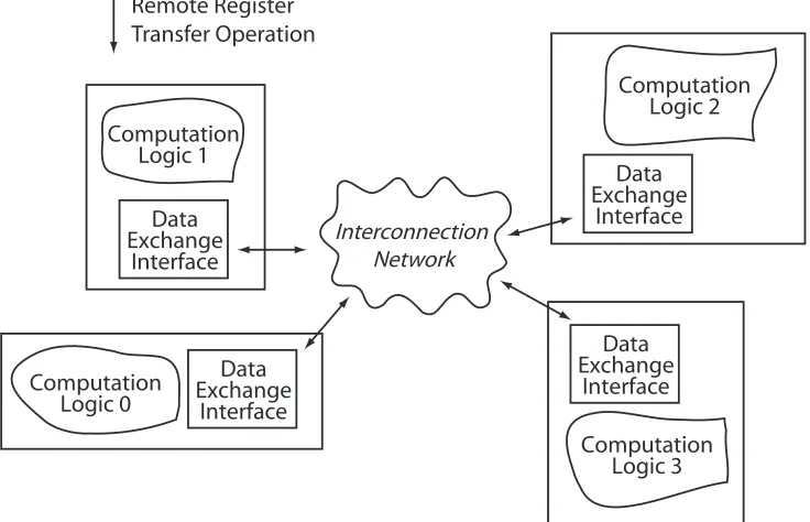
limita-tions and bottlenecks include operating system and data movement overheads. Data movement overheads are introduced as data must be moved between the network and the FPGA hardware computation microarchi-tectures. In directly networked FPGAs, data can be directly exchanged between FPGAs limiting the data movement overhead. This approach was demonstrated by Underwood [Underwood '02] for use on Beowulf [Sterling '95] clusters with the FPGA used to support the network operations and also providing the distrib-uted computation logic. Refining the work of Underwood, the use of FPGAs as the sole element of a larger cluster has become an area of active research. In these FPGA clusters, the FPGA is a compute node in its own right within a larger cluster, consisting of both FPGAs and computers, all interconnected across a net-work. To provide this FPGA cluster architecture, the FPGAs support the distributed hardware application microarchitecture and the remote register transfer operations which allow for the parallelisation of an algo-rithm across the hardware computation resources of the FPGAs.
Computation
Logic 1
Computation
Logic 2
Computation
Logic 3
Computation
Logic 0
Data
Exchange
Interface
Data
Exchange
Interface
Data
Exchange
Interface
Data
Exchange
Interface
Remote Register
Transfer Operation
[image:26.595.93.461.280.517.2]Interconnection
Network
Figure 2: Multiple interconnected FPGA application microarchitectures. Data is exchanged between the computation logic microarchitectures using remote register transfers which are
supported through the data exchange interface.
5 of 257
approaches including high speed point-to-point networks [Comis '05, Brennan '07] and switched Ethernet networks [Fallside '00, Creedon '09b]. The predominant use of Ethernet within the Top500.org [SC '09] along with a ready upgrade path between standards has lead to its use within this project. This coupled to the limited research on the use of switched networking to support distributed hardware applications between in-terconnected FPGAs provide the motivation for using switched Ethernet. Switched Ethernet also fits more readily with message passing than shared memory where message passing applications are more tolerant of higher latency networks [Liu '03a].
This thesis focuses on the message passing parallel programming model and is concerned with how a hardware application microarchitecture interfaces with the synchronisation and data exchange services that need to be on the FPGA to support remote register transfer operations. Synchronisation services ensure the distributed microarchitectures are able to exchange data between each others’ application registers. In the distributed microarchitecture approach, all compute units operate asynchronously to each other requiring synchronisation operations to ensure data can be exchanged correctly. Once nodes are synchronised, the sending and receiving logic of both microarchitectures need to be active to support the remote register trans-fer operation. These constitute services that are needed to support remote register transtrans-fer between the dis-tributed application microarchitectures. The hardware application interface supports these operations, reliev-ing the application programmer of havreliev-ing to implement them and rather allows them focus on the logical parallelisation of the algorithm across the available hardware resources. Through the use of a hardware Application Programming Interface (API), the programmer is abstracted from how these services are imple-mented and also from the architecture of the interconnected FPGAs – switched Ethernet, point-to-point links, etc.. This means different implementations to providing the message passing services on FPGAs are possi-ble, once the hardware API is not changed. The reconfigurability of FPGAs allows for both a dedicated hard-ware message passing and communication microarchitecture or a softhard-ware FPGA processor microarchitec-ture, with an FPGA processor the predominant approach [Saldaña '06a, Sass '07, Pedraza '08] to implement the message passing operations even though hardware communication FPGA microarchitectures have dem-onstrated network performance advantages all be it without a parallel programming model [Underwood '02, Jaganathan '03, Nüssle '07, Schlansker '07]. Each approach has unique advantages and disadvantages to im-plementing message-passing-based remote register transfer operations and within this work, the differences and operations of each are evaluated to ascertain which is more appropriate given an algorithms communica-tion and computacommunica-tion requirements.
1.1
Research Statement
FPGAs provide an application acceleration platform, however FPGAs as a hardware resource have an upper limit to the amount of resources an application can use. If an applications resource requirements exceed that of a single FPGA, the application will need to be run across many independent FPGAs each performing as-pects of the applications computations. This approach requires the exchange of data between FPGAs and this thesis sets out to investigate if an:
FPGA cluster architecture using Message Passing and switch Ethernet is a realistic, feasible and scalable architecture for performing remote register transfer operations between distributed hardware application microarchitectures.
To measure this, the following criteria and approaches are proposed:
• Dedicated hardware and dedicated software solutions to provide the message passing and switched Ethernet communication mechanisms so that comparisons to related solutions can be made. • Each approaches performance in terms of overheads (latency, bandwidth, etc.) to exchange data
across a range of switched Ethernet interconnects. These will be compared against other practical approaches for interconnecting FPGAs.
• The resource overheads of each solutions in terms of FPGA area and the amount of flexibility that is supported along with how these can influence the style of application that can realistically han-dle.
• The independence of the application and associated communications approach based on the provi-sion of a scalable, parameterisable API to abstract the various distributed, independent hardware computation microarchitectures from the communication mechanisms. The ease of use and pro-grammability is also a feature that will be evaluated as part of the API.
1.1.1
Motivation
7 of 257
the distributed microarchitectures and exchange data securely without needing to know the minute details that support the exchange of data. When an algorithm is implemented across multiple microarchitectures that do not operate synchronously with each other, there is a need to ensure they synchronise with each other to perform a register transfer operation. The API provides these operations along with the exchange of data between the distributed registers of the microarchitecture.
Interconnection
Network
FPGA
Management
Node
FPGA
FPGA
FPGA
Algorithm
Figure 3: Parallel Algorithm Mapping Overview. Depicted is the mapping of an algorithm across interconnected FPGAs, with each FPGA using message passing to exchange data between specific
hardware application microarchitecture instances running on each FPGA.
The ability to take an algorithm implemented for a single FPGA and easily and efficiently map it across multiple, distributed and interconnected FPGAs provides the motivation for this work, with Figure 3 depicting a high level view of this idea. Part of the motivation is the choice of interconnect that will support the exchange of data. To allow for scalability and a range of diverse algorithms, investigations into a scal-able interconnect is undertaken. This is the reason for choosing Ethernet, switched Ethernet in particular, as the interconnect between the FPGAs. Ethernet provides scalability through the use of commodity switches which can be configured to support arbitrary numbers of Ethernet enabled devices. Ethernet is a standards-based interconnect which has become a ubiquitous communication medium. Further, it has been demon-strated on a number of occasions that FPGAs are able to support Ethernet as the communication medium [Fallside '00, Brebner '02, Creedon '08]. However, Ethernet is not without its flaws; one of which is that it has a high latency for the exchange of data between interconnected devices. The presence of this latency necessitates the use of a programming model unaffected by this overhead. Message passing is more tolerant of the latencies introduced by the interconnect than shared memory is.
taken is the motivation in this work for the development and comparison of the hardware microarchitecture and the software FPGA processor across a single interconnect solution so that a direct comparison can be performed between each approach. By looking at both approaches, the suitability of switched Ethernet as the interconnection medium for supporting remote register transfer operations between distributed microarchitec-tures can be measured and results compared with other FPGA cluster solutions. To help measure the suitabil-ity of switched Ethernet, a number of criteria are investigated including:
• The reconfigurable overheads required for each message passing architecture • The architecture’s ability to use the parallel hardware of an FPGA to its fullest • The remote register transfer overheads measured in latency and bandwidth.
When combined, the motivation of this work is to look at providing an easy to use parallel pro-gramming model which an application developer can use to perform remote register transfers between dis-tributed microarchitectures running on multiple interconnected FPGAs. The use of switched Ethernet as the only interconnect between the FPGAs is novel and has not been done in this manner before even though switched Ethernet is the predominant interconnect used by cluster computing [SC '09]. Using a single com-modity interconnect also allows for directly interfacing FPGA application microarchitectures and networked computers, enabling them to exchange data with each other. This allows the FPGAs to be treated as peers on the network rather than the more classical view of FPGAs as computation co-processors. Within this work, investigations into the use of FPGAs as complete peers on the network is limited as the focus is on providing a message passing programmers’ interface which can be used to exchange register data between distributed application microarchitectures.
1.1.2
Research Structure
The research for this thesis has been undertaken to further develop existing processes for the parallelisation of algorithms across interconnected FPGAs through the provision of an easy to use and programmer oriented hardware interface which abstracts the application from the physical interconnect and communication opera-tions. For this, there are a number of distinct sections to the research:
1. The first sees the development of the abstract application interface which will support the exchange of data between the distributed application microarchitectures. This interface required the develop-ment of an appropriate Hardware Description Language Message Passing Application Programming Interface (HDL MP API). This interface supports the abstraction of the application from the meth-ods used to exchange data between distributed hardware application microarchitectures.
9 of 257
microarchitecture solution and a software FPGA processor solution have been developed and tested on interconnects of varying capacity with a view to identifying the optimal solution.
3. The third section involves comparative testing of both interconnection solutions for the processing of a variety of algorithms with a view to identifying characteristics of each approach that lend them-selves to particular algorithm types.
4. Finally, as part of the development of the communication strategies, a new and novel algorithm for the exchange of small amounts of data has been developed. The applicability of this algorithm for a range of communication architectures is also undertaken.
1.1.3
Peer reviewed publications
Eoin Creedon, Michael Manzke, “Impact of Fragmentation Strategy on Ethernet Performance”, in Proceed-ings of the 6th IFIP/IEEE International Conference on Network and Parallel Computing (NPC ‘09), 2009 [Creedon '09a]
Muiris Woulfe, Eoin Creedon, Ross Brennan, Michael Doyle, Michael Manzke, “Programming Models for Reconfigurable Application Accelerators”, in Proceedings of the 1st Workshop on Programming Models for Emerging Architectures held in conjunction with the 18th International Conference on Parallel and Compila-tion Techniques (PACT ’09), 2009 [Woulfe '09]
Eoin Creedon, Michael Manzke, “Software vs. Hardware Message Passing Implementations on FPGA clus-ters”, in Proceedings of Parallel Computing with FPGAs, held in conjunction with the 13th International Con-ference on Parallel Computing (ParaCo2009), 2009 [Creedon '09b]
Eoin Creedon, Michael Manzke, “Scalable High Performance Computing on FPGA Clusters Using Mes-sage Passing”, in Proceedings of the 18th IEEE International Conference on Field Programmable Logic and Applications (FPL), 2008 [Creedon '08]
Eoin Creedon, Ross Brennan, Michael Manzke, “Towards a Scalable Field Programmable Gate Array Cluster for Interactive Parallel Ray-Tracing”, in Proceedings of Eurographics Ireland Workshop, 2006 [Creedon '06]
1.1.4
Contribution
FPGAs while through the use of an API supports remote register transfer operations between the microarchi-tectures. To reduce the complexity of interfacing application microarchitectures with the message passing remote register transfer operations, a hardware description language interface has been developed. This al-lows the hardware microarchitecture to request and perform remote register transfer operations without re-quiring knowledge of how the transfer will ultimately be performed, knowing only that the transfer will be performed securely and reliably. The use of switched Ethernet, message passing and distributed FPGAs in this manner has not previously been performed and along with the design and implementation of the message passing application interface forms the main contribution of this thesis.
Through the use of the message passing programming model and distributed, interconnected FPGAs, the contribution of this work sees the use of a hardware application interface which can be used by distributed application microarchitectures to exchange data between remote registers and memory elements. This ensures an algorithm can be parallelised and operated across the available resources of multiple inter-connected FPGAs. Further to supporting the parallelisation of an algorithm across multiple interinter-connected FPGAs, additional contributions of this work include evaluations of the performance overheads of both a hardware message passing microarchitecture and a software FPGA processor microarchitecture. The contri-bution from each of these relates both to how they perform in exchanging data between distributed applica-tion microarchitectures and to how they implement the operaapplica-tions to exchange the data. Through the use of the common application interface, it has been possible to evaluate both implementations using the same hardware microarchitectures, further highlighting the benefit and contribution of using a hardware interface between the application microarchitecture and the message passing exchange mechanisms.
When exchanging data across Ethernet, a means must be provided to split large messages into smaller network-specific data fragments. The unique nature of the implementation platform allowed for evaluations of different approaches to support this data fragmentation operation and ultimately resulted in a novel approach. This contribution formed the basis for a publication [Creedon '09a] and showed that by re-evaluating some of the more common approaches in network communication, performance advantages can be achieved at minimal application implementation cost. The use of this updated fragmentation algorithm is an additional contribution while the ability of the API to shield an application from low level network opera-tions was further tested during these experiments.
1.2
Thesis Structure and Layout
11 of 257
From the information presented in Chapter 2, Chapter 3 details the design requirements that need to be addressed when implementing a message passing, switched Ethernet FPGA cluster. These details are pre-sented in an implementation-independent manner providing a high-level overview. This design has been implemented, and Chapter 4 presents the implementation details. Certain features are common between the hardware and the software solutions. These are detailed along with any updates that have been applied to them, mainly an Ethernet controller update from 10/100Mb to Gigabit operations. Individual implementation details of the hardware and the software solutions are presented, highlighting how they are configured.
Using the design and implementation from Chapter 3 and Chapter 4, experiments have been per-formed to test the research question. As part of these tests and experiments, a number of publications have been generated [Creedon '08, Creedon '09a, Creedon '09b] and all results are presented in Chapter 5. The experiments include benchmarks of the two architectures, allowing for a direct comparison of each approach and also against their ability to support distributed hardware application microarchitectures, the message passing parallel programming model and switched Ethernet. These experiments concentrate mainly on point-to-point operations although some collective operations requiring more than two nodes are performed and the results evaluated. While performing the high level design, a novel approach to data communication was de-vised for performing data fragmentation. Detailed experiments looking at the fragmentation approach on a number of system architectures are evaluated and the results for these presented. The different systems in-clude standard PCs using a custom communication protocol based on that used between the FPGAs and also an approach using Transmission Control Protocol/Internet Protocol (TCP/IP) communication. Finally, ex-periments evaluating the performance of the HDL MP API interface are undertaken using an algorithm de-manding high performance, matrix multiplication.
13 of 257
Chapter 2
Background and Related Work
The research question as presented in Chapter 1 has evolved from a large number of different projects that have looked at various aspects related to this research but not focused specifically on using switched Ethernet in conjunction with message passing as the means to support distributed hardware application microarchitec-tures across interconnected FPGAs. These related fields include parallel computation, FPGA application acceleration, network communication acceleration and application parallelisation across multiple intercon-nected FPGAs. This chapter investigates these areas of research to provide the motivation and developmen-tal approach for interconnected FPGAs.
The first area of relevance is parallel algorithms and the requirements these place on both a compute node and communication mechanisms. To help understand the general requirements of these applications, software PC based approaches are detailed before discussing approaches and implementations that are practi-cal for exchanging data between distributed application logic. PC based solutions are presented initially as these represent the most mature environment which supports the operations that will be required for distrib-uted FPGA hardware application microarchitectures. Parallel programming models are also discussed to show how data can be exchanged by the application. As part of the details on parallel programming models, different interconnect solutions are discussed as they pertain to why switched Ethernet would be used and also what other approaches may be practical. These details aid in understanding the general field that is be-ing researched in this thesis and gives an overview of the requirements that a distributed hardware application will expect of a message passing, switched Ethernet solution.
data between distributed hardware application logic is also detailed. FPGAs have demonstrated different approaches for supporting network communications and these approaches along with configurations that are relevant refine the approach that can be taken as part of the system design and experimental implementation.
Finally, details on other comparable solutions are presented to help put the work of this thesis into context with what others are researching. This helps show the originality and contribution of this work while also detailing comparable solutions which allows the research question to be addressed, is the use of switched Ethernet as the interconnect between distributed FPGA hardware application microarchitectures a good or bad approach to take.
2.1
Parallel Algorithms
Parallel algorithms detail the computations and communications that are performed across multiple compute units in solving an algorithm. Fork-Join is one approach used to perform parallel algorithms where a single processing unit performs all sequential operations before forking the data and operations across multiple compute units to perform the calculations in parallel [Smith '03, Patel '06]. Once the parallel calculations are completed, the results are joined back into a single compute unit which continues the sequential operations before performing any future fork-join parallelisation operations. Fork-join describes the control approach that is used by the parallel implementation of an algorithm but does not describe how data is moved between the sequential and parallel aspects of the algorithms. The data exchange operations that are used depend on the architectural approach and structures that the algorithm is being implemented on, with either a message passing or shared memory approach applicable for the parallel algorithm implementation. In the operation of a fork-join algorithm, data exchange occurs in three separate instances.
1. The movement of data between the sequential aspect of the algorithm and the parallel compute units.
2. The movement of data between the parallel computation units where data can be exchanged between the compute units depending on the algorithm requirements.
3. Data communications between the parallel compute units and the sequential aspect of the algorithm as part of the join operation.
15 of 257
SP and BT look to measure specific features of parallel architectures e.g. parallel I/O performance and how it affects the computation of the system.
'94], depending on the computation iteration. Two communication approaches are possible in a parallel im-plementation. The first uses a data transpose operation before data segments are sent to different compute units. The second sees the use of a butterfly exchange mechanism that sees successive iterations transfer data between more distant compute units. IS computations sort a large integer space and test the integer computa-tion operacomputa-tions of a compute node in conjunccomputa-tion with the communicacomputa-tion performance as data is exchanged continuously with associated nodes [Quinn '94]. LU, SP and BT applications test a larger range of opera-tions than just the computaopera-tions or the network, with the BT benchmarks having a higher degree of I/O based operations to the other approaches. LU and SP algorithms are special sparse matrices which have data dis-tributed across the diagonal and are used in numerical analysis and linear algebra.
Fork-join algorithms require support for interleaving both sequential and concurrent operations to function correctly. Sequential operations require the use of a single, central compute unit which manages and maintains knowledge about the overall results of the computations while concurrent operations see the direct exchange of data between compute units. Support for this style of operation will be required to ensure cor-rect and efficient support of parallel computation across the distributed FPGA hardware application microar-chitectures. The NPB highlight features that are expected of parallel algorithms including the ability to sup-port different data sizes for computations and communications along with the ability to supsup-port a range of different communication topologies. These features will need to be integrated into the FPGA implementation as part of the API so that a range of applications will be supported and not just a limited set. As part of the API, no distinction should be made between compute unit types as the need to exchange data with either a sequential or concurrent compute unit will be needed. To help answer the research question, measuring these operations will help say if switched Ethernet FPGA clusters are able to meet the demands of parallel compu-tation in a realistic and suitable manner.
2.1.1
Parallel Algorithm Communication Patterns
The parallel algorithm implementations in the NPB exchange data with other compute units to perform all algorithm operations. The pattern of these communications are either structured, where the order of the communications is known in advance and does not change during the algorithm execution or is unstructured where for a given iteration in the algorithm it is not known which node has communicated with which node.
17 of 257
for the message passing implementations of the benchmark algorithms. They look at the communications that are performed in an algorithm to see if code optimisations can be applied to improve communication operations. They divide the communications based on dynamic or static and point-to-point or collective communication operations as defined at application compile time. Point-to-point communications account for the vast majority of operations while although collective communications are used by algorithms, they do not account for a large portion of the data or a large number of operations. The average amount of data in communications across all algorithms is approximately 43.6 KB with a range between 1.8KB and 191KB. This information and that of Riesen show that during the execution of an algorithm, it is not possible to know at all times and for all sizes which computation units are exchanging data, necessitating the need for support of a dynamic communication pattern and range of exchange sizes which scales as the number of nodes scales.
Vetter and Mueller [Vetter '03] detail the communication requirements for a number of non-NAS Message Passing Interface (MPI) scientific applications and similarly show a large number of point-to-point communications. Vetter and Mueller present a more detailed breakdown of the communication sizes than Faraj and Yuan and show a point-to-point packet size range between 90 bytes and 533 KB against an overall average of approximately 1.5 KB. The collective communications that are performed only exchange small amounts of data on the order of bytes, not kilobytes. The work of both Faraj and Yuan [Faraj '02] and Vetter and Mueller [Vetter '03] show that a wide range of communication sizes are required by a range of parallel applications. Further to the communication operations and sizes, communication patterns also play a role in how data is exchanged between nodes. As well as the interface supporting variable sized communications, the communication pattern as detailed by Faraj and Yuan [Faraj '02] is predominantly dynamic and unstruc-tured in nature meaning the communication pattern is not known at algorithm compile time but rather based on operations that will occur during algorithm execution.
2.2
Parallel Programming on Microcomputers
While details on fork-join and iterative approaches to solving parallel algorithms show what happens, how an application can use these features needs to be discussed. The use of programming models aid the application developer in expressing the computations and communications that are required while well designed and developed parallel programming models should abstract the programmer from the underlying complexities of how these are performed. This leads to the need for an easy to use, scalable parallel programming model which supports the exchange of data between various, distributed compute units, matching up with the fea-tures that have already been defined – dynamic communication patterns and sizes, variable numbers of com-pute units, etc.. The exchange of this data ensures all computations for a given algorithm are performed cor-rectly. The exchange of data between the distributed compute units can be supported in a number of ways, either explicitly as part of a message exchange operation or implicitly where data is shared between multiple units which can each access it [Werstein '03, SC '09]. Support for the exchange of data between units comes in a number of manners but is typically supported through the use of an API which abstracts the implementa-tion details from the programmer. This allows the programmer to focus on the computaimplementa-tions and data distri-bution operations to make the algorithm operate efficiently in parallel without needing to know how the physical exchange of data will be performed. Both message passing and shared memory have different APIs because of differences that exist in how data is exchanged between compute units and operations that need to be supported. With the introduction of MPI [Forum '95], a single standardised API for message passing has been possible while OpenMP [OpenMP '07] has started to become a standardised API for shared memory but as yet no dominant API for shared memory exists.
The message passing paradigm uses defined messages for internode communication which are then exchanged between the compute units. Message exchange functions are used by an application to generate communications but apart from scheduling the communication to start, no control is in place as to when the exchange will physically occur or complete. No memory space is shared in a message passing system, rather all computation data is stored locally and encapsulated as messages when data is to be exchanged between compute units. The message passing API allows an application assert message exchange functions between interconnected compute units while also abstracting the programmer from the physical communication mechanisms that are used. The programmer concentrates on the parallelisation of the algorithm without needing to be concerned with how the message is generated and exchanged for a given platform [Forum '95]. In message passing systems, two types of message communications are defined, point-to-point and collective communications. Point-to-point communications exchange data between individual compute units using Send and Receive operations. Collective communications occur when a number of compute units are ex-changing messages as one communication operation e.g. a broadcast where one compute unit sends data to all connected compute units.
19 of 257
compute unit accessing it. The location of data is dependent on how it is initially laid out in memory, with some approaches yielding better results as data is stored locally compared with others where more communi-cations can be necessary to access data. Where message passing is concerned with writing programs that exchange messages across an interconnect, shared memory systems are concerned with accessing memory which is shared between the compute units. The memory sharing operations can be achieved in a number of ways, with the two most common being Uniform Memory Access (UMA) and Non-Uniform Memory Access (NUMA). UMA creates a single large memory such that all accesses to memory, regardless of the node that is performing the access has the same overhead. This approach makes the access time uniform and does not suffer from concerns with how data is initially laid out across memory. NUMA on the other hand suffers from non-uniform access times resulting in more efficient access to local memory than remote memory. As part of a NUMA architecture, the memory which nodes access does not need to be local, allowing for Distributed Shared Memory (DSM) environments where data is distributed across interconnected compute units [Karl '99]. Unlike the message passing approach, all accesses in the shared memory approach are based on memory operations, with the amount of data accessed on a per communication basis being less than that exchanged in message passing. A shared memory API needs to support the sharing of memory between compute units and also reading and writing operations that are possible to this memory. To ensure data sta-bility and prevent corruption, memory locking operations are needed which enforce a single compute unit accessing the data at a time.
This thesis is looking at message passing as opposed to shared memory for a variety of reasons in-cluding the existence of a pre-defined API which supports the message passing programming model. As well as the API – MPI – further reasons message passing is being researched include the fact that the API ab-stracts the user from the physical communication implementation that is used allowing a hardware applica-tion microarchitecture to exchange data locally with different compute units on the same FPGA or across an interconnect to distributed compute units. This thesis is only concerned with using message passing to ex-change data between distributed hardware application microarchitectures however, the use of message pass-ing to exchange data between different compute units on the same FPGA has been demonstrated by others, [Saldaña '06a, Williams '06, Ziavras '07], and details on their work is discussed in Sections 2.6 and 2.7. In developing the message passing communication interface, a hardware API will need to be developed and the features that this API requires have been detailed in Section 2.1 with more specific operations detailed in this section. As no specific hardware message passing API exists, these interface operations need to be known so that a robust and useful interface is developed.
2.2.1
Message Passing
in-compatibilities between the codes of the different systems, making portability difficult. This posed a problem as the message passing operations on the different systems were very similar in how the algorithm was paral-lelised and implemented [Gropp '93]. To address this, a number of approaches were developed which looked to hide the differences of the physical implementations of the systems. One of the early investigations into this was the development of Parallel Virtual Machine (PVM) [Sunderam '90, Geist '94] which developed a complete control and operation environment to support the exchange of data between compute units. This still required the different systems to support the PVM model for correct operation. To address code port-ability concerns between different message passing systems, the MPI working group was setup [Dongarra '93] which created and standardised MPI [Forum '95] as a portable message passing API. MPI portability stems from its adoption by all major vendors as the message passing parallel programming model while the development of MPICH [Gropp '96] as a compliant MPI solution further aided adoption. MPI defines the API that is used to exchange messages between co-operating compute units. It does not specify explicit im-plementation approaches, leaving that to individual imim-plementations. Support for MPI styled communica-tions will aid the hardware API as MPI communication patterns should be transferable to the hardware API without requiring much if any modifications.
When the specification of MPI was being developed, the MPICH system was created to test and check the various MPI operations that were being proposed in order to define problems and concerns that could arise [Gropp '96]. As MPICH was the first implementation of MPI and to ensure it could be easily adopted for use on different compute clusters, a layered approach to its implementation was taken. This en-abled support for different interconnects without needing to modify higher layers of the message passing op-erations that are supported. To support this, all platform-dependent opop-erations are encapsulated by the Abstract Device Interface (ADI) [Gropp '94]. The use of the ADI allowed for the quick development and porting of MPICH to a wide range of compute clusters while not preventing more tuned versions which inter-face at different layers in MPICH to improve performance. Since MPICH, a wide range of MPI compliant systems have been developed and implemented including Local Area Multicomputer (LAM)/MPI [LAM '09], OpenMPI [Gabriel '04], MVAPICH [University '09], Fault-tolerant Embedded MPI (FEMPI) [Subramaniyan '06], Embedded MPI (eMPI) [McMahon '96], Lightweight MPI (LMPI) [Agbaria '06], Toronto Molecular Dynamics-MPI (TMD-MPI) [Saldaña '06a] and others. Most development has been for microprocessor-based solutions which use a standard processor for the communication operations although some specialised implementations do exist for dedicated environments e.g. eMPI [McMahon '96], TMD-MPI [Saldaña '06a].
hard-21 of 257
ware. LAM/MPI [LAM '09] is a new implementation of MPI which does not use MPICH code. This results in a different implementation philosophy with LAM/MPI looking to leverage the performance of cluster computers more natively than MPICH. This is achieved by using daemons running on the compute units to create the MPI communication environments. LAM/MPI also implements Interoperable MPI [IMPI '00] which allows different implementations of MPI to communicate correctly with each other through the use of bridging devices which translate between the different MPI implementations. Like MVAPICH before it, LAM/MPI supports acceleration logic present on Infiniband, Myrinet and other high performance networks. OpenMPI [Gabriel '04] is a new and updated version of LAM/MPI merging efforts from Los Alamos (LA)-MPI [Aulwes '04, LA-(LA)-MPI '09] and Fault Tolerant-(LA)-MPI [Fagg '00, FT-(LA)-MPI '09] to create a more robust and fault tolerant MPI implementation meant for 10’s of thousands of nodes. The addition of fault-tolerance with MPI code is driven by the scale of modern MPI clusters, into the 10’s of thousands, where the number of compute units increases the likelihood of a failure. For scientific computations, a compute unit failure if not handled correctly would prevent the application from completing properly. OpenMPI addresses this by using a modular implementation approach which allows it to load the components on a case by case basis, reducing the memory footprint and the MPI implementation complexity.
Further to the approaches detailed above, a number of embedded processor approaches have been developed. eMPI [McMahon '96] looks at extending MPICH into the embedded processor domain. eMPI takes two approaches for implementing MPI as part of an embedded processor cluster, the first looking at removing unnecessary or costly aspects of MPICH for embedded processors e.g. memory requirements. The second is a ground up, custom implementation which is built for the resources of the embedded processor specifically. Comparisons on the two approaches show that although the custom solution outperforms the MPICH implementation both in performance and memory footprint, the overall time to implement it can outweigh the possible performance advantage. A further concern raised by the custom solution of eMPI is that while it operates correctly, it is not portable across embedded processors as each processor has distinct features and operations which will not be present on all devices. FEMPI [Subramaniyan '06] and LMPI [Agbaria '06] are two other MPI implementations for the embedded domain. FEMPI [Subramaniyan '06] is concerned with the implementation of a fault tolerant MPI system for embedded processors. They present architectural considerations for embedded systems that need fault tolerance with the main concern being the amount of resources the system can spare to perform both the fault tolerant operations and maintain efficient computations. LMPI [Agbaria '06] is concerned with a lightweight MPI implementation for distributed em-bedded devices. To achieve this, a subset of MPI is run on emem-bedded processors while a microprocessor server runs a complete MPICH version to exchange data with other MPI enabled systems and performs trans-lations to LMPI as required. All LMPI communications between embedded devices are based on exchanging data with the server node with no direct communications supported between devices.
and synchronisation operations of the compute units. The communication layer performs the actual commu-nication operations for exchanging the data between the compute units on the interconnect. The operations are split in this manner as exemplified by the ADI interface of MPICH [Gropp '94] to ensure different, more agile communication approaches can be used as either hardware or network performance allows. The devel-opment of network offload architectures where communication operations can be performed at the network interface has seen the modification of message passing implementations, aided by the layered approach, to take advantage of these architectures [Dalessandro '05b]. The use of updated network and communication operations is exemplified by the introduction and use of network communication offload logic where opera-tions are performed on the network card or by separate, dedicated communication processors [Adiga '02]. The development of communication offload logic is driven by issues and performance concerns that are pre-sent in cluster computing using standard communication protocols. This sections discussion on various MPI implementations has been used in formulating an approach for the design, development and implementation of the message passing architecture for this thesis. The two approaches that are detailed are either a layered approach that communicates directly with other message passing systems (MPICH, MVAPICH) or a daemon based approach where additional resources are set aside on a device to support the message exchange opera-tions (LAM/MPI, OpenMPI). As the resources of an FPGA will be limited and to better support the use of a message passing hardware microarchitecture, a layered approach is being used with the message passing op-erations built on top of the communication opop-erations. From the need to support both point-to-point and col-lective communications, the layered approach also better lends itself to this as the colcol-lective communications can be layered on top of the point-to-point communications. From the approaches of MVAPICH, LAM/MPI and others, the use of the FPGA to accelerate the communication operations will be investigated and details on the types of operations that can be accelerated are discussed in Section 2.2.4. The use of a layered ap-proach will also allow the FPGA implementation to best use the resources that are available to it for a given operation rather than constricting its operations.
2.2.2
MPI
23 of 257
Point-to-Point Communications
Point-to-Point communications are used to directly exchange data between nodes on an individual basis, in-dependently of the operations of other nodes. The main point-to-point communication methods are Send, Receive, and Send_Receive. Send is used to send data from one node to another directly, with a node identi-fied by a node identity integer which is unique on all nodes. An appropriate receive must be asserted at the destination node to ensure the communication completes correctly. Send and receive operate independently of each other and each must be called when required. Send_Receive is used to assert both the sending and receiving logic concurrently. Associated with the point-to-point communications, are communication modes and communication style. Three communication modes are defined for both sending and receiving. These modes are synchronous, buffered, and ready. Synchronous mode communications complete onc