TA 7.4
Phase-state Low Electron-number Drive
Random Access Memory (PLEDM)
Kazuo Nakazato, Kiyoo Itoh1, Haroon Ahmed2, Hiroshi Mizuta, Teruaki Kisu3,
Masataka Kato4, Takeshi Sakata1
Hitachi Cambridge Lab Hitachi Europe Ltd., Cambridge, U.K.
1Central Research Labs Hitachi Ltd. Tokyo, Japan 2Cavendish Lab Cambridge Univ., Cambridge, U.K. 3Hitachi ULSI Systems Co. Tokyo, Japan 4Semiconductor Division, Hitachi Ltd. Tokyo, Japan
Dynamic random access memories (DRAMs) based on a transistor/capacitor cell are used as main memories in computers because of their high capacity and high speed. Since there is no gain in the present DRAM cell, it requires a large cell-capacitor to produce an adequate sense signal. In each new memory generation, structure and fabrication have become more complicated to main-tain a large capacitor while miniaturizing the cell.
This phase-state low electron-number drive memory (PLEDM) gain cell uses a stacked tunnel transistor (PLEDTR) [1]. Since this cell has gain, a large capacitor is not necessary. The cell size is 5F 2 where F is the minimum feature size. Its read and write times are simulated as 20ns and 5ns, respectively. In principle, it is possible with PLEDM to have a retention time longer than 10 years, enabling a non-volatile memory to be realised [2].
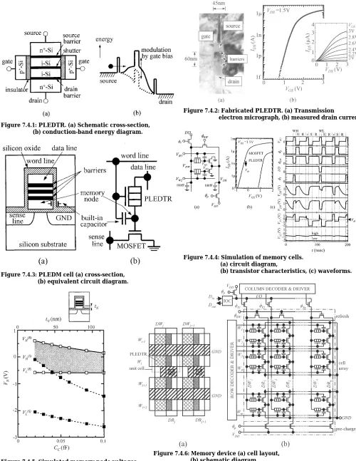
PLEDTR is a vertical fully depleted double-gate SOI-MOSFET with barriers in the channel region (Figure 7.4.1). Gate voltage modu-lates the internal potential in the intrinsic silicon region and the central shutter barrier or barriers (CSB) move up and down ener-getically following the internal potential. The CSB reduce OFF current substantially, while keeping device ON current high. The device may be regarded as a three-terminal version of the heterostructure hot-electron diode (H2ED) based on transition from a tunneling current to a thermoionic emision current at a semicon-ductor heterojunction [3]. The role of the source and drain barriers is (1) to increase the weighting of the high-energy part of the injected electrons (2) to act as impurity diffusion barriers which ensure a low impurity level within the channel, and (3) to reduce leakage current such as gate-induced drain leakage current at the drain side.
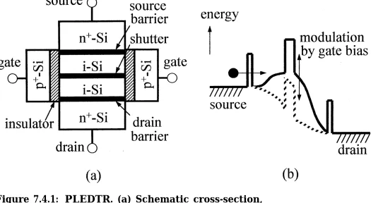
PLEDTRs with triple tunnel barriers are fabricated on silicon dioxide using a standard silicon process, as shown in Figure 7.4.2. All transistor regions, source, drain, channel, and gate, are poly-crystalline-silicon films. The thin tunnel junctions are formed by thermal nitridation of silicon at 900oC. Source and drain regions are heavily phosphorous doped to 2x1020cm-3, while the channel region is maintained at impurity level <1017cm-3 as confirmed by SIMS analysis. The gate is boron doped to 5x1019cm-3. The channel length is 60nm and the gate insulator is formed by 6nm of silicon dioxide. The gate separation width is 45nm, and the gate width, perpendicu-lar dimension to the plane of Figure 7.4.2a, is 0.4µm.
Drain current measurements shown in Figure 7.4.2b demonstrate <1fA leakage. The threshold voltage is ~1V, and sub-threshold voltage slope S is 96mV/decade. This sub-threshold voltage slope is explained well by the scaling theory for a double-gate SOI MOSFET [4], and the same slope S is obtained for PLEDTR with the 0.2µm gate separation and 350nm channel length [5].
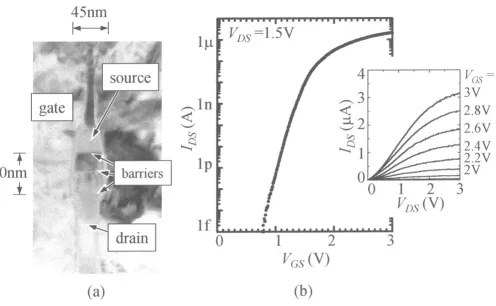
PLEDTR enables construction of high-density memory because each memory cell occupies the area of one transistor, as shown in Figure 7.4.3. A PLEDTR is stacked onto the gate of a conventional MOSFET with a built-in coupling capacitor to realize a memory cell. High-speed write is possible by transferring electrons from the top
electrode (data line) onto the memory node through the ON-state PLEDTR. Since the OFF-state PLEDTR effectively confines elec-trons, the stored information can be kept for a long time without refresh. Since the information is read via the current in a MOSFET, this cell has gain and a large S/N ratio.
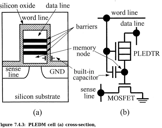
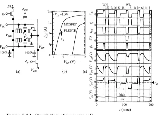
Storage, read, and write cycles are all controlled by voltage Vw on the word line, VW(S) (-2V), V
W
(R) (0.5V), and V W
(W) (3V). (Figure 7.4.4) The generation of negative word line voltage is described in reference [6]. In the storage cycle the built-in coupling capacitor CC causes the memory node voltage VN to be lower than the threshold voltage Vth of the sense MOSFET. In the read cycle VN becomes higher than Vth when the memory state is high and lower than Vth when the memory state is low. In the write cycle the PLEDTR is opened, and VN becomes the data line voltage, 1.5V for the high memory state and 0V for the low memory state. Figures 7.4.4(b) and (c) show the results of mixed-level device and circuit simulation of two memory cells using 0.13µm rules. A sequence of writing high state (WH), storage (S), read (R), refresh (r), S, R, writing low state (WL), S, R, r, S, R, with 10ns/20ns/5ns storage (pre-charge) /read/write time is simulated. VDD =1.5V. Vw2 is kept at -2V (unselected) after writing high or low state. The refresh inverts the memory state. The inverting cell concept is described in reference [7]. Although the drain-source current in the ON state of a PLEDTR is ~1µA, write is fast because of the reduced stored charge, which is determined by the gate capacitance of the sense MOSFET and estimated as 0.2 to 0.3fC. On the other hand a high ON current is available from the sense MOSFET to drive the data-line capacitance, 200fF in this simulation.
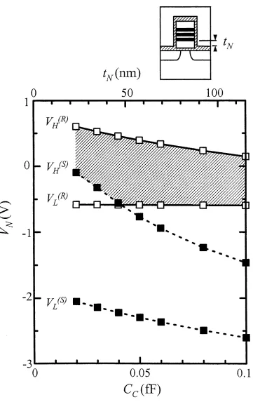
The memory node voltage VN in the storage and read cycles is calculated as a function of the coupling capacitance CC in Figure 7.4.5. VH(R) and V
L
(R) are in the read cycle in high and low memory states, respectively. VH
(S) and V L
(S) are in the storage cycle. The voltage difference on the memory node between high and low memory states, VH-VL, can be larger than the writing voltage difference, 1.5V in this case, because of the change of memory node capacitance between inversion and depletion states of the sense MOSFET. Random read access in a cell array is possible when Vth is set in the hatched area, for example, between 0.5V and –0.5V at 0.04fF coupling capacitance. This coupling capacitance can be real-ized for a 50nm thick memory node (tN), without needing to form an additional capacitor.
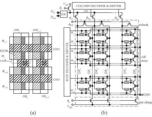
The 5F 2 memory cell layout is shown in Figure 7.4.6a. The schematic of memory device is shown in Figure 7.4.6b. The refresh circuit consists of one transistor per column with the same pitch as the memory cell, without sense amplifiers, so the cell area occupancy ratio increases substantially. An experimental memory cell array is in fabrication.
References:
[1] Nakazato, K., P. J. A. Piotrowicz, D. G. Hasko, H. Ahmed, K. Itoh, “PLED – Planar Localised Electron Devices”, IEDM, pp.179-182, 1997.
[2] Mizuta, H., K. Nakazato, P. J. A. Piotrowicz K. Itoh, T. Teshima, K. Yamaguchi, T. Shimada, “Normally-off PLED (Planar Localised Electron Device) for non-volatile memory”, VLSI Symposium, pp. 128-129, 1998. [3] Hess, K., T. K. Higman, M. A. Emanuel, J. J. Coleman, “New ultrafast switching mechanism in semiconductor heterostructures”, J. Appl. Phys. 60, pp. 3775-3777, 1986.
[4] Suzuki, K., T. Tanaka, Y. Tosaka, H. Horie, Y. Arimoto, “Scaling theory for double-gate SOI MOSFET’s”, IEEE Trans. Electron Dev., ED-40, pp. 2326-2329, 1993.
[5] Kisu, T., K. Nakazato, “Silicon Stacked Transistor with Source and Drain Tunnel Barriers”, ESSDERC, pp. 532-535, 1999.
[6] Tanaka, H., M. Aoki, T. Sakata, S. Kimura, N. Sakashita, H. Hidaka, T. Tachibana, K. Kimura, “A Precise On-Chip Voltage Generator for a Gigascale DRAM with a Negative Word-Line Scheme”, IEEE JSSC 34, pp.1084-1090, 1999.
• 2000 IEEE International Solid-State Circuits Conference
07803-5853-8/00
©2000 IEEE
[image:2.603.71.571.66.713.2]Figure 7.4.6: Memory device (a) cell layout, (b) schematic diagram. Figure 7.4.5: Simulated memory node voltages.
Figure 7.4.4: Simulation of memory cells. (a) circuit diagram,
(b) transistor characteristics, (c) waveforms. Figure 7.4.3: PLEDM cell (a) cross-section,
(b) equivalent circuit diagram.
Figure 7.4.2: Fabricated PLEDTR. (a) Transmission
electron micrograph, (b) measured drain current. Figure 7.4.1: PLEDTR. (a) Schematic cross-section,