USER'S MANUAL FOR
MSC 8C)09
Infcrmaticn contained in this manual is disclosed in confidence and may not be duplicated in full or in part by any person without priolr written approval of Mcneli thic Systems
Corporation. Its sole purpcse is to provide the user with adequately detailed documentation so as to efficiently install, operate', maintain, and order spare parts for the system supplied. The use of this doc~~ent for all other purpcses is specifically prohibited.
C:OPYRIGHT
©
1980 BY MONOLITHIC SYSTEMS CORPORATION84 In~erness Circle East Englewood, Colorado, 80112
(303) 170-7400
PRELIMINARY 2-26-81
1 . 1 1 . 2 1 . 3 1 . 4 1 . 5 1 . 6 1 . 7 1 . 8
1 . 9 1 .10 1 . 11 1 . 12
1 . 13
1 • 14
SCOPE
SPECIFICATIONS
FUNCTIONAL DESCRIPTION Z80A PROCESSOR
MSC 8009 TABLE OF CONTENTS
SECTION 1 INTRODUCTION
ARITHMETIC PROCESSING UNIT (Optional) 1. 5. 1 9511 APU
1. 5. 2 9512 APU BUS INTERFACE
MODE STATUS REGISTER
1.
7.
1 Bus Exchange Modes READ/WRITE MEMORY1. 8. 1 Refresh Cycle READ ONLY MEMORY
1. 9. 1 Protection PROM
DUAL MAP CONFIGURATION (Optional) I/O INTERFACE
1.11. 1 Serial I/O Interfaces FLOPPY DISK INTERFACE
1.12. 1 Disk Format
~.12. 2 Status Register
1.12. 2. 1 Address Marks
1.12. 2. 2 Cyclic Redundancy Check Characters (CRC) INTERRUPT
1.13. 1 Non-Maskable Interrupt SYSTEM CONTROL
1.14. 1 System ~lock
1.14. 2 Power Up
1.14. 3 Memory And I/O Addressing 1.14. 4 Watchdog Timer
2. 1 2. 2
2. 3 2. 4
2. 5
2. 6
SCOPE
INSTRUCTION AND DATA FORMAT ADDRESS MODES
SECTION 2
zao
PROCESSOR2. 3. 1 Branching Instructions 2. 3. 2 Restart Instruction (RST) FLAG
2. 4. 1 2. 4. 2 2. 4. 3
Carry Flag (C)
Add/Subtr' act Flag (N) Parity/Overflow Flag (P/V)
2. 4. 3 .. 1 Arithmetic Operations 2. 4. 3 .. 2 Logical Operations 2. 4. 4 Half-Carry Flag (H)
2. 4. 5 Zero Flag (Z) 2. 4. 6 Sign Flag (S) OP CODE SUMMARY
2. 5. 1 Mnemonic Operand Symbols 2. 5. 1. 1 8-Bit Operation 2. 5. 1~ 2 16-Bit Operation
2. 5. 2 Flag Symbols
2. 5. 3 8-Bit Data Transfer Group 2. 5. 4 16-Bit Data Transfer Group
2. 5. 5 Exchanget Block Transfer and Search Group
2. 5. 6 8-Bit Ari.thmetic And Logical Group
2. 5. 7 General Purpose Arithmetic And Control Group 2. 5. 8 16-Bit Arithmetic Group
2. 5. 9 Rotate And Shift Group
2. 5.10 Bit Set, Reset And Test Group 2. 5.11 Program Transfer Group
2. 5.12 Call And Return Group 2. 5.13 Input/Output Group OPCODE FORMAT AND DESCRIPTION
2. 6. 1 8-Bit Data Transfer Group
2. 6. 2 16--Bit Data Transfer Group
,.. 6. 3 Exc!hange, Block Transfer And Search Group 2. 6. 4 8-Bit Arithmetic And Logical Group
2 .. 6. 4. 1 Arithmetic Instructions 2 .. 6. 4. 2 Logical Group
2. 6. 5 General Purpose Arithmetic And Control Group
2. 6. 6 16-Bit Ar'ithmetic Group
2. 6. 7 Rotate And Shift Group
2. 6. 8 Bit Set, Reset And Test Group
2. 6. 9 Program Transfer Group
2. 6.10 Call And Return Group 2. 6.11 Input/Output Group
3. 1 SCOPE
SECTION 3
MULTI BUS
3. 2 MULTIBUS CONVENTION 3. 3 MULTIBUS CONTROL
3. 3. 1 Bus Contention Resolution
3.. 3. 1. 1 Serial Bus Priority
3. 3. 1. 2 Parallel Bus Priority 3. 3. 1. 3 Bus Exchange Modes
3. 3. 2 Acknowledge Signals
3. 3. 2. 1 Transfer Acknowledge (XACK/) 3.. 3. 2. 2 Advance Acknowledge (AACK/)
3. 4 SPECIFICATIONS
3. 4. 1 Electrical Characteristics 3. 4. 2 Mechanical Characteristics 3. 4. 3 Signal Description
3. 4. 4 Data Transfer Timing 3. 5 MSC 8009 CONFIGURATION
Figure 3- 1
Figure 3- 2 Figure 3- 3 Figure 3- 4 Table 3- 1 Table 3- 2
4. 1 SCOPE
SERIAL-BUS CONTENTION CONFIGURATION Z80 READ OPERATION
Z80 WRITE OPERATION
MULTI BUS DATA TRANSFER TIMING MULTI BUS LEVEL SPECIFICATIONS MULTI BUS ELECTRICAL REQUIREMENTS
SECTION 4 MEMORY
4. 2 R~~ CONFIGURATION 4. 2. 1 Addressing 4. 2. 2 Memory Read 4. 2. 3 Memory Write 4. 2. 4 Refresh Cycle 4. 3 EPROM/R~1 CONFIGU HATION
4. 3. 1 EPROM/HOM Addressing 4. 3. 2 Memory Protect
SECTION 5 SERIAL I/O INTERFACE
5. 1 SCOPE 5- 1
5. 2 CONFIGURING THE SERIAL I/O PORT 5- 1
5. 2. 1 Terminal/Communication Configuration 5- 1 5. 2. 2 Programmable Timer Configuration 5- 1 5. 2. 2. 1 BAUD Rate Configuration 5- 5
5. 2. 3 Clock Configurations 5- 5
5. 2. 4 EIA RS·-232-C Configuration 5- 6
5. 2. 5 TTL Conflguration 5- 6
5. 2. 6 Current. Loop Operation 5- 1
5. 2. 1 Interrupt Configuration 5- 1
5. 3 PROGRAMMING THE SERIAL I/O INTERFACE 5- 9
5. 3. 1 Initialization 5- 9
5. 3. 2 Clock Set 5- 9
5. 3. 3 Control ~lord Programming 5- 9
5 .. 3. 3. 1 Mode Instruction 5-11
5. 3. 3. 2 Command Instruction 5-11
5. 3. 4 Status Word Format 5-13
5 .. 3. 4. 1 Parity Error 5-13
5. 3. 4. 2 Overrun Error 5-14
5 .. 3. 4. 3 Framing Error 5-14
5. 4 DATA COMMUNICATION 5-14
5. 4. 1 Asynchl"onous Transmission 5-14
5. 4. 2 Asynchronous Receive 5-14
5. 4. 3 Synchronous Transmission 5-15
5. 4. 4 Synchr onous Rece i ve 5-15
5. 5 TIMER INTERFACE 5-17
5.5. 1 JJJode Definitions 5-18
5 .. 5. 1. 1 HODE 0 - Interrupt On Tenninal Count 5-19 5.. 5. 1. 2 MODE 1 - Progralmnable One Shot 5-20 5. 5. 1. 3 MODE 2 - Rate Generator 5-21 5. 5. 1. 4 MODE 3 - Square Wave Generator 5-22 5. 5. 1. 5 MODE 4 - Software Triggered Strobe 5-23 5. 5. 1. 6 MODE 5 - Hardware Trigger Strobe 5-24
5. 5. 2 On-The--FlY Readout 5-25
5. 5. 3 BAUD Rate Generator 5-25
Figure 5-Figure 5- 2 Figure 5- 3 Figure 5- 4 Figure 5- 5 Figure 5- 6 Figure 5- 1 Figure 5- 8 Figure 5- 9 Figure 5-10 Figure 5-11 Figure 5-12 Figure 5-13
CONTROL WORD SEQUENCE
MODE INSTRUCTION CONTROL WORD FORMAT COMMAND INSTRUCTION CONTROL WORD FORMAT STATUS WORD FORMAT
SYNC CHARACTER TRANSMISSION
8253 INTERVAL TIMER CONTROL WORD FORMAT MODE 0 TIMING DIAGRAM
MODE 1 TIMING DIAGRAIJJ MODE 2 TIMING DIAGRAM MODE 3 TIMING DIAGRAM MODE 4 TllV1ING DIAGRAM MODE 5 TIMING DIAGRAM
BAUD RATE GENERATOR ROUTINE
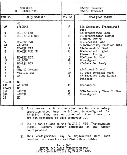
Table 5- SERIAL 1/0 CABLE CONNECTION FOR DATA COM~1UNICATIONS EQUIPMENT (DCE) Table 5- 2 SERIAL 1/0 CABLE CONNECTION FOR
DATA COMMUNICATIONS EQUIPMENT (DTE) Table 5- 3 SERIAL I/O PORT CONFIGURATION
Table 5- 4 PRCXJ RA]-1MABLE TIME R SIGNALS Table 5- 5 8253 TIMER PORT ADDRESSES
Table 5- 6 8253 TIMER REGISTER BAUD RATE VALUES
SECTION 6
FLOPPY-DISK FORMATTER/CONTROLLER
6. 1 SCOPE
6. 2 DESCRIPTION
6. 3 CONTROL REGISTERS
6. 3. 1 Command Hegister
6. 3. 1. 1 Unit Register 6. 3. 1. 2 Command Register 6. 3. 2 Status Register
6. 3. 3 Track Register 6. 3. 4 Sector Register 6. 3. 5 Data Register 6. 4 COMHAND STRUCTURE
6. 4. 1 Head Positioning Commands (Type 1) 6. 4. 2 Sector Comnands (Type 2)
6. 4. 3 Track Commands (Type 3) 6. 4. 4 Reset Interrupt (Type 4) 6. 4. 5 Write Precompensation 6. 5 FORMATTING THE DISK
6. 6. 1 Shugart Drives
6. 6. 1. 1 Gaps
6. 6. 1. 2 Address Marks
6. 6. 1. 3 Cyclic Redundancy Check Character 6. 6. 1. 4 Setting Up The Disk
6. 6. 2 IBM Format
Figure 6- 1 Figure 6- 2 Figure 6- 3 Figure 6- 4 Figure 6- 5
6. 6. 2. 1 IBM 3740 (Single Density) 6. 6. 2. 2 IBM System 34 (Double Density)
COMMAND FtOUTINE STATUS REGISTER READ DISK SECTOR FORMAT
TRACK SEEK FROM TRACK 00 TRACK SEEK
Table 6- 1 Table 6- 2 Table 6- 3
Table 6- 4 Table 6- 5 Table 6- 6 Table 6- 7
7. 1 SCOPE
DRIVE DESIGNATION HEAD POSITION STATUS READ/WRITE STATUS
FLOPPY-DISK COMMAND SUMMARY
FORMATTER/CONTROLLER CONTROL BYTES GAP DEFINITIONS
ADDRESS MARK DEFINITION
SECTION 7 INTERRUPT
7. 2 Z80 INTERRUPT CONTROL
7. 3 8214 INTERRUPT CONTROLLER 7. 3. 1 Initialization 7. 3. 2 MULTIBUS Interrupt
7. 3. 3 Progranming Multi-Level Interrupts 7. 4 8214 PRIORITY INTERRUPT CONTROLLER
7. 4. 1 Address And Bit Assignments 7. 4. 2 Vectors
7. 5 NON-MASKABLE INTEHRUPT (NMI)
Table 7- 1 DATA BIT FUNCTIONS FOR OUTPUT TO INTERRUPT CONTROU.ER (Device Code D7)
8. 1 SCOPE
8. 2 SYSTEM DESCRIPTION
SECTION 8 THEORY OF OPERATION
8. 2. 1 Local Control Bus
8. 2. 1. 1 MULTIBUS Control 8. 2. 2 Local Address Bus
8. 2. 2. 1 MULTIBUS Addressing 8. 2. 3 Data Channel
8. 2. 4 Z80 Processor
8. 2. 5 Floppy Disk Formatter/Controller 8. 2. 6 Arithmetio Processing Unit (APU) 8. 2. 7 System Clock
8. 3 SYSTEM OPERATION
8. 3. 1 Wait Operation
8. 3 .. 1. 1 Watchdog Timer
8. 3. 2 OP Fetch Cycle
8. 3. 3 Memory Read Or Write
8. 3. 3. 1 Address Decoding
8. 3. 4 1/0 Cycles
8. 3. 4. 1 Arithmetic Processor Cycles
8. 3. 5 Disk Formatter/Controller
8. 3. 5. 1 Register Selection
8. 3. 5. 2 Clock Circuit
8. 3. 5. 3 Data Exchange
8. 3. 5.4 Disk Read 8. 3. 5. 5 Disk Write
8. 3. 5. 6 Head Loading Delay 8. 3. 6 Acknowledge Cycle
8. 3. 7 Interrupt Request
8. 3. 7. 1 Non-Maskable Interrupt 8. 3. 8 HALT Request
8. 3. 9 System Reset 8. 4 SYSTEM CONTROL
8. 4. 1 Bus State Machine
[image:8.621.83.525.34.655.2]8. 4. 1 .. 1 Bus Exchange 8. 4. 2 Memory State Machine
Figure 8- 1 Table 8- 1 Table 8- 2
9. 1 SCOPE
8. 4. 2. 1 Refresh Z80 MICROPROCESSOR
CLOCK RATE CONFIGURATION
SYSTEM CONTROL PROM SIGNAL IDENTIFICATION
SECTION 9
ARITHMETIC PROCESSOR UNIT
g. 2 CAPABILITIES
9. 2. 1 I/O Addressing 9. 3 9511 ARITHMETIC PROCESSOR UNIT
9. 3. 1 Initialization 9. 3. 2 Stack Control 9. 3. 3 Data Format
9. 3. 3. 1 Command Format 9. 3. 3. 2 Status Register
9. 4 9511 INSTRUCTIONS
9. 4. 1 Data And Stack Manipulation Operations g. 4. 2 16-Bit F:ixed-Point Operations
9. 4. 3 32-Bit F:ixed-Point Operations
9. 4. 4 32-Bit Floating-Point Primary Operations 9. 4. 5 32-Bit Floating-Point Derived Operations 9. 5 9511 OP CODE FORM1\T:S
9. 6 9512 ARITHMETIC PROCESSOR UNIT 9. 6. 1 Stack Control
9. 6. 1. 1 Double Precision 9. 6. 2 Co~~and Format
9. 6. 3 Status Register 9. 7 9512 INSTRUCTIONS
9. 7. 1 Data And Stack Manipulation Operations 9. 7. 2 Single Precision Operations
9. 7. 3. Double Precision Operation 9. 8 9512 OP CODE FORMLATS
Figure 9- 1
Table 9- 1 Table 9- 2 Table 9- 3
Appendix A Appendix B Appendix C Appendix D
303-0271-000 305-0271-000
9511 INITIALIZATION SEQUENCE
STACK CONFIGURATIONS STATUS BIT DEFINITION STACK CONFIGURATIONS
APPENDICES
MSC 8009 PIN ASSIGNMENT MSC 8009 JUMPER REQUIREMENT FLOPPY-DISK JUMPER CONFIGURATION 9511 APPLICATION NOTE
DRAWINGS
MSC 8009 BOARD LAYOUT MSC 8009 SCHEMATIC
[image:9.611.84.497.38.648.2]SECTION '1 INTRODUCTION
1.1 SCOPE
The Monolithic Systems Corporation MSC 8009 is a single-board OEM computer that is dlirectly compatible with the industry standard MULTIBUS* . As software development is a major cost of any computer system, the 8080 software compatibility of the MSC 8009 provides an advanced, high-speed, next-generation system without incurring the costs and delays associatedl with developing new software. New systems can now be designed taking full advantage of the Z80A* instruction set and optional floating-point arithmetic unit.
The MSC 8009 operates in a multimaster system with either parallel or serial priority resolution. An on-board bus plus the MULTIBUS structure allows other operations to proceE~d on the MULTIBUS while the Z80A processor uses local memory and 1/0 devices. Since the on-board memory and 1/0 resources are extensive, bus access is usually needed only for communication between tasks. System throughput with multiple masters is greatly enhanced because of the light MULTI BUS traffic load. MULTIBUS compatibility means that the MSC 8009 can be used either to expand existing SBC 80-based systems or as the basis of a new design.
An on-board floppy-disk formatter/controller in addition to two serial ports will increase' the computing power for most applications. Via a 17q3 Floppy-Disk FormatterlController, the floppy-disk interface of the MSC 800Q offers a soft-sector format that can be made IBM compatible with the proper softw'are. Variable length sectors and the self-clocking feature of the 1793 means more data per track. The system uses Z80 block 1/0 instructions to transfer data. Write pre-compensation reduces error rate; and the data separator is crystal controlled. Programmable stepping rates from 3 to 15 milliseconds lets the MSC 8009 operate with drives having different track-to-track access time.
*MULTIBUS is a registered trademark of Intel Corporation
1.2 SPECIFICATIONS
PROCESSOR:
Z80A (4 MHz)
MULTIBUS COMPATIBILITY:
Full MULTIBUS control logic permits up to 16 bus masters (including other MSC CPU's) to share the system bus.
BUS EXCHANGE MODES:
Three bus modes allow exchange of bus master every cycle, every instruction (allows test and set), or never. The program sets the bus modes for optimum control of multi-processing systems.
CYCLE TIME:
The execution of the fastest Z80A instruction require 1.25 microseconds.
FLOPPY DISK INTERFACE: Format:
Accomodates single- and double-density formats that are compatible with IBM soft-sector configuration. Read Mode:
Single/multiple sector read with automatic search or entire track read. Either selectable 128 byte or variable length sector.
Write Mode:
Single/multiple sector write with automatic search. Entire track write capability for diskette formatting. Supporting Software:
CP/M
9511 FLOATING
POINT AlU
8214 INT[RRUPT CONTROllER
&
yrCTOR PR(JIt
rlOPPV D[',!'
[10 r:ONNF r. TOR
!len
rlOPPY O[<:;K
CONTROllER
DIV IOrR
STAT[ MACHINE
~.[ RIAL
1/0 CONNfnOR
8253
TIMER lJSART
i
l80n! PROCESSOR
<;[RJAI J 10 r.o~mF r. TOR
USART
CLOCK
16MHI
DYNAMIC RAM
32K
ROM/EPROM
4K, BK, 16K or 3
Capability:
With proper drive options, up to eight 4- or 8-inch disk drives intermixed can be controlled.
Model Compatibility:
The models listed can be accommodated. However, other drives can be used and have not been included.
MEMORY CAPACITY:
Shugart SA-400 Shugart SA-450 Shugart SA-800 Shugart SA-850
RAM - 32K bytes, dynamic
EPROM - The MSC 8009 is shipped with four sockets that accomodate most 8-bit wide memory devices with standard 24-pin callout. Capacities include:
1) To 32K using 8K x 8 masked-ROM elements. 2) To 16K using 4K x 8 EPROM elements. 3) To 8K using 2K x 8 EPROM elements. 4) To 4K using 1K x 8 EPROM elements.
MEMORY MANAGEMENT:
RAM and ROM addressing under PROM control Dual-address map option provides two, selectable under program control.
on 1K-byte boundaries. complete address maps
MEMORY PROTECTION:
A protection PROM allows the selection of system resources that are available to other MULTIBUS masters. Any or all of the RAM, ROM or
1/0 subsystems may be protected from external access. MEMORY REFRESH:
The memory refresh cycles are automatic and nearly transparent.
DIRECT MEMORY ACCESS:
Another bus mastE~r may access the on-board memory or 1/0 devices (if allowed by the protection PROM) :in 625 to 750 nanoseconds.
FLOATING POINT ARITHt1ETIC:
Two optional Arithmetic Processing Units are available -- the 9511 and the 9512 .. The 9511 provides 32-bit precision fixed or floating point operations including transcendental functions. For increased performance, the 9512 offers 32- and 64-bit arithmetic operations. INTERRUPTS:
Vectored, 8-levels of priority interrupts plus Non-Maskable Interrupt (NMI). All on-board interrupt sources are open collector so that a number of devices can share the same level.
Two serial ports provide a programmable interface that can be used for either synchronous or asynchronous operation. One port can be configured for Ed ther EIA RS-232-C, TTL or opto-isolated 20 mA loop signals. The other port can be configured for EIA RS-232-C or TTL only. Signal specifications are:
Synchronous:
5- to 8-hit character; one or two programmable SYNC characters.
Asynchronous ::
5- to 8-bit character; 1, 1-1/2, or 2 stop bits; choice of parity or error detection.
BAUD Rates:
TIMERS:
One 16-bit counter/timer with six operational modes.
MODE 0 - Interrupt
MODE 1 - Programmable/Retriggerable One-shot
MODE 2 - Pulse Rate Generator MODE 3 - Squarewave Generator MODE 4 - Software Triggered Strobe MODE 5 - Hardware Triggered Strobe MODE 6 - Baud Rate Generator for
one serial port
INTERFACE SIGNALS:
MULTIBUS:
All signals conform with MULTIBUS specifications.
Floppy Disk 1/0:
All signals are TTL compatible.
Serial 1/0:
Signals fulfill either EIA RS-232-C, TTL or 20 rnA current loop convention depending on the MSC 8009 configuration.
Interrupt Requests:
All signals are TTL compatible.
Timer:
All signals are TTL compatible.
POWER REQUIREMENTS:
The MSC 8009 operates with MULTIBUS power supply voltages of +5V, -5V, +12V, and -12V.
100-0123-001
PHYSICAL DIMENSIONS:
12 in.(Width) X 6.75 in.(Height) X 0.5 in.(Depth).
1.3 FUNCTIONAL DESCRIPTION
The MSC 8009 design is based on the Z80A microprocessor, which is fully upward compatible with the popular 8080A. The Z80A executes all 8080 instructions without mJdification. In fact, there are cases where 8080 progr ams in ROM and PROM can simply be plugged into the MSC 8009 with a significant improvement in performance. However, care must be taken when certain programming techniques have been used in 8080 application programs due to the 4-MHz clock rate of the Z80A. Polling loops or delay-timing routines may require adjustment. An additional flag appears in the flag register for' the BCD subtraction feature. Flag differences may be sign:ificant in rar'e cases where uncommon programming techniques have been employed.
1.4 Z80A PROCESSOR
The Z80A processor itself offers features that are beyond those of the 8080 or 8085. The designer or programner can use these features to reduce system size or further increase the speed of application programs. These features include:
(1) 80 additional instructions (2) Double compliment of registers (3) Block transfer 1/0 instructions (4) Index registers
(5) BCD subtraction
(6) Two additional interrupt modes
(7) Non-Maskable Interr'upt (NMI)
1.5 ARITHMETIC PROCESSING UNIT (Optional)
The MSC 800Q will accept one of two available Arithmetic Processor Units
(APU) •
1 .5. 1 9511 APU
The 9511 enhances the computational capability of the MSC 8009. It is capable of performing 32-bit operations using floating point as well as fixed-point data formats. Data transfers are to or from an internal stack. Commands are issued to a second 1/0 address to perform an operation on the data that is contained in this stack. The status of the 9511 can be read out at any time from the same 1/0 address. The results are then made available for retrieval, or an additional command may be entered. If the 9511 is busy, it will cause the Z80 to wait if the CPU tries to access the 9511.
Some of the arithmetic and transcendental functions in addition to control and conversion commands that can be performed with the 9511 include:
1.5.2 9512 APU
(1) Basic Arithmetic Operations (Addition" Subtraction, Multiplication and Division).
(2) Trigonometric Functions.
(3) Logarithmic Functions (Common and Natural).
(4) Constant Pi ('It) -y' (5) Exponential Functions (e ~ or X ).
(6) Stack Control (single, double or floating).
(1) Square Root.
(8) Change Signs (single, double or floating).
The 9512 provides single-precision (32-bit) and double-precision (64-bit) add, subtract, multiply and divide operations. All operand result, status and command information transfers take place over an 8-bit bidirectional data bus. Using programmed I/O, the user can handle all data transfers between the Z80 and the 9512. Operands are pushed onto an internal stack by the Z80; and a command is issued to perform an operation on the data stack. By popping the stack, the final result is then made available to the Z80.
1.6 BUS INTERFACE
The MSC 8009 uses an internal bus for access to the on-board memory, arithmetic processor, floppy-disk formatter/controller and I/O. Since these on-board tasks do not require the MULTIBUS, the MSC 8009 is able to perform internal operations and not interfere with the MULTIBUS activities. This means that up to 16 bus masters (including other MSC 8009' s) can share' thE~ MULTIBUS and provide the user with the benefits of multiprocessing.
1.7 MODE STATUS REGISTER
An internal 8-bit register sets up the MSC 8009 via software control for the following indicated modes of operation.
~I_O_7~~IO_6
__+-I_O~ I~~IO_3
____~_02
__~
______ IOO __MEMORY HAP INTERRUPT MODE
1.7.1 Bus Exchange Modes
INTERRUPT PRIORITY BUS EXCHANGE MODE
Through program control, the user can use bits 4 and 5 (104 and 105) to select one of three bus modes for optimum control of a multiprocessing system. These modes are:
105 104
0 0
0
BUS OPERATION
Bus released to higher priority on every data transfer.
1.8 READ/WRITE MEMORY
In the basic system, the dual-ported dynamic RAM provides the MSC 8009 with up to 32K-byte storage capacity_ The sixteen-chip memory array is partitioned into two, 16K-byte sections. Either the address lines of the Z80A processor or the MULTIBUS (Direct Memory Access) address these arrays. The refresh cycle of the dynamic RAM is automatic. So that requested memory operations can be performed with minimum time delay, the refresh cycle is hidden.
1.8.1 Refresh Cycle
If either a memory read or write operation of the dynamic RAM is in progress, the refresh cycle is inhibited. When the memory cycle is complete, a refresh cycle may be initiated. The refresh control logic attempts to initiate a refresh during an M1 machine cycle, making the refresh transparent. However, if an M1 cycle is not available, the refresh is still inserted.
1.9 READ ONLY MEMORY
Four ROM/EPROM sockets accommodate the most popular 8-bit wide, 24-pin memory devices. These devices normally hold the commonly used subroutines, standard support software and programs for specific applications. By using the 2108 and 2158 (1K X 8EPROM), the MSC 8009 can hold up to 4K bytes of program storage. The 2516 or 2116 (2K X 8 EPROM) provides 8K bytes while either the 2532 or 2132 4K X 8 EPROM offers the user 16K bytes. For 32K byte capacity, the user can use the 8K X 8 masked ROMs.
Since each ROM/EPROM device may vary in power configuration, hardware jumpers provide the required voltages. Different chips may be intermixed, but three of the four sockets must contain the same devices. For example, standard support software may require three 2116's (2K X 8 EPROM) and one 8K X 8 Masked ROM -- total capacity of 14K bytes.
1.9.1 Protection PROM
A special PROM protects any or all RAM, ROM or I/O subsystems from external access. This device generates an internal enabling signal that permits the bus to address the MSC 8009 only when called for. A pin on the auxilliary connector totally disables access to the MSC 8009 board, allowing multiple processors to be paged into the same memory space.
1.10 DUAL MAP CONFIGURATION (Optional)
The optional DUAL MAP feature provides the MSC B009 with two complete address maps. The system always powers up using the first map. Since the system has to have a ROM at location zero to start properly, a ROM should be mapped into low memory. For example, the user can switch to a map that contains RAM in low memory. This is achieved through a bit sent with the same output instruction used for programming the interrupt controller (See paragraph 1.7). A "0" in bit position six represents a s tart up condition :, and a " 1" switches the map. This capabi Ii ty permits the use of soft.ware written for BOBO and ZBOA processors that previously could not be run on a single-board computer.
1.11 I/O INTERFACE
Two serial 110 interfaces provide the MSC B009 with serial-data communication channels that are programmable and will operate either synchronously or asynchronously based on the current serial-data transmission protocols. The floppy disk interface can support up to eight soft-sector drives. Since an address decoder PROM defines the MSC BOOQ address structure, any 1/0 device on-board may be assigned any of the 256 device address codes used by the BOBO or ZBOA instruction set. 1.11.1 Serial 110 Interfaces
The two serial 110 interfaces are designed around two software-programmable devices -- an 8251 USART (Universal/Asynchronous Receiver/Transmitter) and an B253 Prograrrnnable Timer. The user can configure one channel only for either EIA RS-232-C, TTL or opto-isolated 20 rnA current-loop operation. The other channel can be configured for either EIA RS-232-C or TTL operation.
NOTE: For current loop operation, supplies the current source for
the external device proper operation.
1.12 FLOPPY DISK INTERFACE
An onboard chip allows the MSC 8009 to interface with up to eight 4- or
8-inch drives intermixed. The commands listed in the following Table Can be used to perform the desired floppy-disk operation.
1.12.1 Disk Format
Restore Seek Step Step In Step Out Read Sector Write Sector
Read Address Read Track Write Track
Disks may be formatted to be compatible with either Shugart drives, IBM 3740 or System 34 formats with Sector lengths of 128, 256, 512, or 1024 bytes.
Basically a recorded sector on disk consists of two fields -- the ID FIELD and the DATA FIELD. The ID FIELD contains the ID Address Marks, track number, side number, sector number, sector length, and the Cyclic Redundant Check bits (CRC). The information contained within the ID FIELD must be found within four revolutions of the disk; otherwise, a "record-not-found" condition will be set up. The sector length defines the number of bytes per sector.
The DATA FIELD consists of its Address mark, data and CRC bits. For double-density operation, there will be three bytes preceding the Address Marks of the ID FIELD and DATA FIELD with the clock transition missing between bits 4 and 5.
1.12.2 Status Register
An 8-bit Status Register, internal to the formatter/controller chip, provides the user with the status of the floppy-disk operation. During the execution of a command, a status bit will be set, which can be monitored. This bit is reset when the current instruction terminates. The remaining bits are updated in accordance to the instruction.
1.12.2.1 Address Marks
For synchronization, each track clock bits called "Address Marks".
has a unique combination of data and These four distinct marks are:
Index ID Address Data Address Deleted Address
1.12.2.2 Cyclic Redundancy Check Characters (eRC)
All information beginning with an address mark and up to the actual CRC characters themselves establishes the contents of the Cyclic Redundancy Check characters. Each field recorded on disk is appended with two CRC character bytes. These bytes are generated from a cyclic permutation of the data bits starting w:i th bit zero of the address mark and terminating with bit zero of the last byte within a field (excluding CRC bytes). When a field is read, the data bits are divided by the same general polynomial. A nonzero remainder indicates invalid data, while a zero remainder denotes that correct data has been read.
1.13 INTERRUPT
The MSC 8009 provides veetoring for eight levels of priority interrupt in addition to a Non-Masl<able Interrupt (NMI). Three operating modes nd priority assignments may be configured anytime during system opertion via software control. 1hese modes include:
(1) MODE 0 generates RST instructions, identical with 8080 vectoring.
(2) MODE 1 vectors all levels to location 38H ( RST7) independent of the interrupt vector hardware. This mode is useful
because all interrupts locat:Lon 38H.
(3) HaDE 2 uses a PROM to specify the eight, low-order bits of interrupt-vector address for each of the eight, priority levels. The Z80A interrupt vector register defines the eight, high-order bits that are set by the program. Consequently, any interrupt can be vectored to any location in memory under program control.
1.13.1 Non-Maskable Interrupt
The Non-Maskable Interrupt (NMI) feature of the Z80A provides the MSC ROOq with an effective and efficient method of dealing with system power failure or for diagnosing certain hardware and software problems. A power-fail service routine can be added to an existing SBC 80 program without major changes because the NMI functions independently of existing interrupt hardware.
A pin of the SBC auxiliary connector P2 is assigned to NMI. Also, NMI may be connected to pin 33 of P1 (MULTIBUS connector), but this is a reserved bus pin and may conflict with some applications. NMI can be used to detect error conditions or abnormal system situations, but should not be used in the course of normal program execution. The power-fail module can make use of NMI so that system status is saved and used for restart information. NMI always vectors to location 66H.
1.14 SYSTEM CONTROL
The majority of MSC 8009 logic is synchronous with the master clock. Additional independent system-timing functions include power up initialization and a Watchdog Timer.
1.14.1 System Clock
The MSC 800q uses a standard, master-clock frequency of 16 MHz to derive the 8-MHz Bus clock. A number of MSC 8009 functions are synchronized with the master clock (K1115A device).
1.14.2 Power Up
When powering up the MSC 8009 for operation, the -5V must be stable prior to applying +12V. During the power down sequence, the +12V must be removed before the -5V.
An open-collector driver produces the initializing signal INIT/. This signal is held for at least 50 milliseconds after power up, conditioning the MSC 8009 for ope:ration. In place of the driver, an external device can also be used to initialize the system via the MULTIBUS.
1.14.3 Memory And 110 Addressing
A bipolar, fusible-link PROM defines the memory address and 110 structure, for the MSC 8009. Jumpers and switches have been eliminated to increase reliability and provide more flexibility in memory allocation. Any memory device may be assigned to start on any 256-byte boundary in the 64K addressable space. The memory and 110 allocations of the standard figure are suitable for most applications. However, if care is taken to avoid overlapping device addresses, the address-decoder PROM contents may be reprogrammed to satisfy even the most unusual memory o)~ I/O address mapping requirements. Two complete address maps may be stor'ed in an optional extended PROM.
1.14.4 Watchdog Timer
SECTION 2 Z80 PROCESSOR
2.1 SCOPE
This section discusses and summarizes the Z80 instruction set that is used in programming the MSC 8009. The instructions are grouped according to the type of instruction. Each instruction is described using the assembly language mnemonic operation code; the instruction name; the symbolic operation; a description; the binary fields and pattern that make up the machine instruction; and the number of memory cycles, machine states and affected flags.
The mnemonic operation codes used here differ in some cases from those used by Zilog so as to be compatible with commonly used 8080 (Intel) mnemonics. The equivalent Zilog operation codes appear to the upper right of each instruction description.
2.2 INSTRUCTION AND DATA FORMAT
The program instruction may be 1, 2, 3 or 4 bytes (8 bits
=
1 byte) in length. A multiple-byte instruction is stored in successive memory locations with the first byte address as the instruction address. The exact format depends on the operation that is to be performed.As with instructions, multi-byte data are stored in successive memory locations with the least-significant byte first.
2.3 ADDRESS MODES
There are four modes of addressing data that are stored either in me:nory or in processor registers.
1) DIRECT Mode uses byte 2 and byte 3 of the instruction to define the desired memory location of the data. Byte 2 contains the low-order bits of the address and byte 3, the high-order bits.
2) REGISTER Mode uses a 2 or 3 bit field in the instruction to specify the register or register pair containing the data.
4) IMMEDIATE Mode uses additional instruction bytes to store the data. Data can be either 8 bits or 16 bits in length (least-significant byte first followed by the most-significant byte).
2.3.1 Branching Instructions
I~ormally t the execution of an instruction procedes sequentially through increasing memory address. However, a branching instruction can specify the address of the next instruction to be executed in one of . two ways. Jumps and Calls are branching instructions.
1) The branch instruction holds the address of the next instruction that is to be executed, where byte 2 contains the low-order address and byte 3 the high-order.
2) The branch instruction defines a register pair that contains the address of the next instruction to be executed. The first register provides the high-order bits of the address and the second, the low-order bits.
An exception to these two cases is the 'RST' instruction. 2.3.2 Restart Instruction (RST)
This is a special 1 byte call instruction that is usually used during interrupt sequences. A 3 bit field in the RST instruction determines one of eight fixed vector addresses. The program control is transferred to the instruction that has an address eight times the contents of this
3 bit field.
2.4 FLAG
The flag regi.ster' (F and F') supply information regarding the Z80 status at any specific time. Bit position for each flag is shown below:
where:
7 6 5 4 3 2 1 0
S Z X H X P/V N C
C = CARRY FLAG
N
=
ADD/SUBTHACT FLAGP/V
=
PARITY/OVERFLOW FLAG (1 indicates even parity). H=
HALF-CARHY FLAGZ
=
ZERO FLAG S=
SIGN FLAG X=
NOT USEDEach of the two
zao
Flag Registers contain 6 bits of status information that are either set or reset by CPU operations. Bits 0, 2, 6 and 7 are testable and used with conditi.onal Jump, Call or Return instructions. Flags Hand N are associated with BCD arithmetic and are not directly testable.2.4.1 Carry Flag (C)
Either an ADD instruction that generates a carry or a SUBTRACT instruction that generates a borrow, sets the CARRY FLAG. This flag is then reset if a carr'y is not generated or a borrow does not occur. This is convenient for extended preclslon arithmetic. Also, the 'DAA' instruction sets the CARRY FLAG if the conditions for a decimal adjustment are fulfllled.
For Rotate and Shift instructions, the CARRY FLAG provides a link between the least.-significant and most-significant bit for any register or memory location. For example, the carry holds the last bit shifted from bit 7 of the register or memory location during a Rotate or Shift Left instruction. For a Rotate or Shift Right, the carry represents bit
o of the register or' memory location.
Logical instruction AND, OR, and XOR reset the CARRY FLAG. Also, the CARRY FLAG can be set through instruction 'SCF' or complemented with
2.4.2 Add/Subtract Flag (N)
The Decimal Adjust Accumulator instruction (DAA) uses the ADD/SUBTRACT FLAG to distinguish between 'ADD' and 'SUBTRACT' operations. For all
'ADD' operations, this flag is reset and for all 'SUBTRACT' operations, this flag is set.
2.4.3 Parity/Overflow Flag (P/V)
The PARITY/OVERFLOW FLAG is set to a specific state that depends on the operation.
2.4.3.1 Arithmetic Operations
An overflow condition sets this flag to indicate that the result in the accumulator is either greater than the maximum number (+127) or less than the minimum number (-128). The sign bit of the operand denotes the overflow condition.
For addition, operands with different signs never cause an overflow condition. When adding operands with like signs, a sum with a different sign sets the PARITY/OVERFLOW FLAG. The following example illustrates this situation.
ADDEND: +120 (decimal)
=
0111 1000 (binary) AUGEND: +105 (decimal)=
0110 1001 (binary) SUM: +225 (decimal)=
1110 0001 (binary)The binary sum represents -95, which is incorrect, therefore the PARITY/OVERFLOW FLAG is set.
An overflow can occur for operands of unlike signs in a subtraction operation. Consider the following example.
MINUEND: +127 (decimal)
=
0111 1111 (binary) SUBTRAHEND:(-)-64 (decimal)=
1100 0000 (binary) DIFFERENCE: +191 (decimal)=
1011 1111 (binary)The minuend sign has changed from a positive to a negative, giving an incorrect difference -- an overflow condition.
Another way to predict overflow is to observe the carry to and from the sign bit. If there is a carry in and no carry out, or if there is no carry in and a carry out, then overflow has occurred.
2.4.3.2 Logical Operations
The PARITY/OVERFLOW FLAG finds use as a parity indicator for logical and rotate operations. The number of "1" bits in a byte are counted and an odd number sets the flag to "0" -- odd parity. If the total is even, the parity flag is set to
"1".
Also, when inputting a byte from an I/O device, certain input instructions affect the parity flag to indicate the parity of the incoming data.2.4.4 Half-Carry Flag (H)
The carry and borrow status between accumulator bits 3 and 4 during an 8-bit arithmetic operation affects the condition of the HALF-CARRY FLAG. The Decimal Adjust Accumulator instruction (DAA) uses this flag to correct the result of a packed BCD add or subtract operation. This flag is set according to the following table.
H
o
2.4.5 Zero Flag (Z)
ADD
There is a carry from bit :3 to bit 4.
There i.s no carry from bit :3 to bit 4.
SUBTRACT
There is no borrow from bit 4.
There is a borrow from bit 4.
If the result when executing an appropriate instruction is 0, the ZERO FLAG is set.. The ZERO FLAG is always "1" if the resulting byte in the accumulator is 0 \.Jhen performing an 8-bi t arithmetic operation. A non-O result resets the flag.
When performing block-compare (search) instructions, a subtract is performed without affecting the accumulator contents. The Z flag is set to a "1" if an equivalence is found between the accumulator value and the memory location pointed to by the contents of the register pair HL. The ZERO FLAG jLndicates the complemented state of specific bits when testing a bit in a memory location or register.
2.4.6 Sign Flag (S)
The SIGN FLAG stores the state of the most-significant bit of the accumulator (bit 7). When the processor performs arithmetic operations on signed numbers, binary two's complement notation is used to represent and process numeric information. A "0" in bit 7 denotes a positive number and a "1ft signifies a negative number. The binary equivalent of a positive number is stored in bits 0 thru 6 for a total range of 0 to 127. The two's complement of the positive number represents a negative number with a total range of -1 to -128. When inputting a byte from an
1/0 device to a register, input instruction INP r, the SIGN FLAG indicates either positive (S
=
0) or negative (S=
1) data.2.5 OP CODE SUMMARY
The following symbols, abbreviations and mnemonics will be used to describe the instruction set with exceptions noted where appropriate. So that the information is easy to use, a shorthand notation is employed for describing the assembler format of the instruction and its actual operation. All capital letters and special characters in the mnemonic descriptions are required. The lower-case characters indicate a class of values that can be inserted in the instruction at that point. A single, lower-case letter indicates an eight-bit quantity or register; while a double, lower-case letter denotes a sixteen-hit quantity or register. A symbol enclosed in parenthesis under the NOTATION heading indicates that the value whose address is specified ·is used.
2.5.1 Mnemonic Operand Symbols
2.5.1.1 8-Bit Operation
BYT CYC PG S b e n i d r rr p s IFF CY ZF v[n] REGISTER A B C D E H L I R M PATTERN DESIGNATION 111 000 001 010 011 100 101 110
NumbE~r of bytes. Number of cycles. Sectton 2 page number. Number of states.
DESCRIPTION
Accumulator B Register C Register D Register E Register H Register L Register
Interrupt Vector Register Refresh Register
Memory Location addressed by HL pair
A bi.t position in an 8-bit byte, where the bits are numbered from right to left 0 to 7.
Relative 8-bit address (-126 to +129). Any 8-bit absolute value.
An index register reference, either X or Y
An 8-bit index displacement where -128<d<127 8-bit register
B for the BC register pair, D for the DE pair, H for the HL pair, and SP for the stack pointer.
interrupt vector number (0-7) Vector Address
o OOH
1 08H
2 10H
3 18H
4 20H
5 28H
6 30H
7 38H
Any of r (defined above) or M. Interrupt flip-flop.
Carry flip-flop. Zero flag.
2.5.1.2 16-Bit Operation
PSW
B
H
SP
PG
PC IX IY zz nn
tt
uu
vvH
vvL
AF Register Pair processor status word BC Register Pair
HL Register Pair
Stack Pointer Register Section 2 page number. Program Counter
X-Index Register Y-Index Register
B for the BC register pair, D for the DE pair. Any 16-bit value, absolute or relocatable.
B for the BC register pair, D for the DE pair, H for the HL pair, and PSW for the A/Flag pair.
B for the BC register pair, D for the DE pair, SP for the stack pointer, and X for index register IX.
B for the BC register pair, D for the DE pair, SP for the stack pointer, and Y for index register IY.
The most-significant byte of the 16-bit value or register vv.
The least-significant byte of the 16-bit value or register vv.
2.5.2 Flag Symbols
X - Flag affected.
* -
Flag unaffected.P - Parity flag affected according to parity result of operation. V - Overflow flag affected according to the overflow result.
o -
Flag reset. 1 - Flag set.? - Flag unspecified.
100-0123-001
2.5.3 8-Bit Data Transfer Group
INSTRUCTION FLAG
NOTATION CYC S BYT
OP CODE PG S Z H P/V N C
MOV r,r' 22 r<=r' 1 4 1
* * * * * *
MOV r,M 22 r<=(HL) 2 7 1
* * * * * *
MOViR d,r ~?2 (i-Ki) <=r 5 19 3
* * * * * *
MOV M,r 23 (HL)<=r 2 7 1
* * * * * *
MOVRi r,d 23 r<=( i-Ki) 5 19 3
* * * * * *
MVI r,n 24 r(=n 2 7 2
*
* * * * *
MVI M,n 24 (HL)<=n 3 10 2
* * * * * *
MVIi d,n 25 (i+d)(=n 5 19 4
* * * * * *
LOA nn 25 I A<=(nn) 4 13 3
*
* * * * *
STA nn 26
I
(nn)<=A 4 13 3
* * * * * *
LOAX zz 26 A<=(zz) 2 7 1
* * * * * *
STAX zz 26 (zz)(=A 2 7 1
* * *
*
* *
LOAI 27 A<=I 2 9 2 X X 0 IFF 0
*
LOAR 27 I A(=R 2 9 2 X X 0 IFF 0
*
STAI 28 I<=A 2 9 2
* * * * * *
2.5.4 16-Bit Data Transfer Group
-INSTRUCTION
NOTATION OP CODE PG
LXI rr,nn 29 rr<=nn LXIi nn 29 i<=nn LBCD nn 30 B<=(nn+1)
C<=(nn) LDED nn 30 D<=(nn+1 )
E<=(nn) LHLD nn 30 H<=(nn+1 )
L<=(nn) LliD nn 32 IiH<=(nn+1)
IiL<=(nn) LSPD nn 30 SPH<=(nn+ 1)
SPL<=(nn) SBCD nn 31 (nn+1)<=B
(nn)<=C SDED nn 31 (nn+1)<=D
(nn)<=E SHLD nn 31 (nn+1)<=H
(nn)<=L SliD nn 32 (nn+1)<=IiH
(nn)<=IiL SSPD nn 31 (nn+1)<=SPH
(nn)<=SPL
SPHL 33 SP<=HL
SPli 33 SP<=Ii
PUSH qq 34 (SP-1)<=qqH (SP-2) <=qqL SP<=SP-2 PUSHi 34 (SP-1)<=iH
(SP-2)<=iL SP<=SP-2 POP qq 35 qqH<=(SP+1)
qqL<=( SP) SP<=SP+2 POPi 35 iH<=(SP+ 1)
iL<=(SP) SP<=SP+2
CYC S BYT
3 10 3
4 14 4
6 20 4
6 20 4
5 16 3
6 20 4
6 20 4
6 20 4
6 20 4
5 16 3
6 20 4
6 20 4
1 6 1
2 10 2
3 11 1
3 15 2
3 10 1
4 14 2
FLAG
~
S Z H P/V N C
2.5.5 Exchange, Bloc~~ Transfer and Search Group
~---~ i
INSTRUCTION
OP CODE
XCHG EXAF EXX XTHL XTli LDI LDIR LDD LDDR CCI CCIR CCO CCDR NOTATION PG
-36 L<=)DE 36 SW<=)PSW' 36
H
P
B H
C DE HL<=)BC'DE'HL'
37 37
38
<=)( SP+ 1)
'L I I
(
<=)(SP) iH<=)( SP+ 1) il<=)(SP) OE)<=(HL) D IE<= DE+1
L<=HL+1
H
B C<=BC-1 38 R
u
epeat LOI ntil BC=O.
39 ( OE)<=(HL) E<=OE-1 'L<=HL-1
D
H
B ,C<=BC-1
39 R epeat LOO
u ntil BC=O 41 A .-( HL)
H B
L<=HL+1 C<=BC-1
111 R epeat CCI until
A .=( HL) or BC=O
llO A .-(HL) 'L<=HL-1
H
B C<=BC-1
llO R 'epeat CCO until
A = (HL) or BC=O
-CYC S
1 4
1 4
1 4
5 19
6 23
4 16
5/4 21/16
4 16
5/4 21/16
4 16
5/4 21/16
4 16
5/4 21/16 BYT 1 1 1 1 2 2 2 2 2 2 2 2 2 FLAG
S Z H P/V N C
•
•
• •
• •
• • •
•
•
•
• • •
•
•
•
•
• •
*
• *
• • *
* • *
• • 0 X
o
*
* *
0 0o
*
* *
0 Xo
*
* *
0 0o
*
X X X X
*
*
X X X X 1
*
X X X X 1
*
2.5.6 8-Bit Arithmetic And Logical Group
INSTRUCTION
NOTATION OP CODE PG
ADD r 42 A<=A+r ADD M 42 A<=A+(HL) ADDi d 43 A<=A+(i+d) ADI n 43 A<=A+n ADC r 43 A<=A+r+CY ADC M 44 A<=A+(HL)+CY ADCi d 45 A<=A+(i+d)+CY ACI n 44 A<=A+n+CY SUB r 45 A<=A-r SUB M 46 A<=A-(HL) SUBi d 41 A<=A-(i+d) SUI n 46 A<=A-n SBa r 41 A<=A-r-CY SBB M 48 A<=A-(HL)-CY SSBi d 49 A<=A-( i+d) -CY SB! n 48 A<=A-n-CY ANA r 54 A<=A&r ANA M 54 A<=A&(HL) ANAi d 55 A<=A&(i+d) ANI n 55 A<=A&n ORA r 56 A<=A!r ORA M 56 A<=A! (HL) ORAi d 51 A<=A! (i+d) ORr n 56 A<=A!n XRA r 51 A<=A"r XRA M 58 A<=AA(HL) XRAi d 59 A<=AA(i+<1) XRI n 58 A<=AAn
CMP r 49 A-r
CMP M 50 A-(HL)
CMPi d 51 A-(i+d)
CPI n 50 A-n
INR r 51 r<=r+1
INR M 52 (HL)<=(HL)+1 INRi d 52 (i+<1)<=(i+d)+1 , DCR r 52 r<=r-1
DCR M 53 (HL)<=(HL)-1 DCRi d 53 (i+d)<=(i+d)-1
CYC S BYT
1 4 1
2 1 1
5 19 3
2 1 2
1 4 1
2 1 1
5 19 3
2 1 2
1 4 1
2 1 1
5 19 3
2 1 2
1 4 1
2 1 1
5 19 3
2 1 2
1 4 0
2 1 1
5 19 3
2 1 2
1 4 1
2 1 1
5 19 3
2 1 2
1 4 1
2 1 1
5 19 3
2 1 2
1 4 1
2 1 1
5 19 3
2 1 2
1 4 1
3 10 1
6 23 3
1 4 1
3 11 1
6 23 3
FLAG
S Z H P/V N C
X X X V
o
X X X X Vo
X X X X Vo
X X X X Vo
X X X X Vo
X X X X Vo
X X X X Vo
X X X X Vo
XX X X V 1 X X X X V 1 X X X X X 1 X X X X V 1 X X X X V 1 X X X X V 1 X X X X V 1 X X X X V 1 X X X 1 P 1 0 X X 1 P
o
0 X X 0 P 1 0 X X 1 Po
0 X X 1 Po
0 X X 1 Po
0 X X 1 Po
0 X X 1 Po
X X X 1 Po
0 X X 1 Po
0 X X 1 Po
0 X X 1 Po
0 X X X V 1 X X X X V 1 X X X X V 1 X X X X V 1 X X X X Vo
*
X X X Vo
*
Xx
X Vo
*
X X X V 1*
X X X V 1
*
X
x x
V 1*
100-0123-0C
2.5.7 General Pul"pos~~ Arithmetic And ContrO'l GrO'up
INSTRUCTION
NOTATION
eye
OP CODE PG
-DAA 60 CO'nvert A to' 1
packed BCD after an add or subtract of packed BCD operands
CMA 60 A<=flA 1
NEG 61 A<=-A 2
CMC 61 CY<=flCY 1
STC 61 CY<=1 1
NOP 62 No OperatiO'n 1
HLT 62 Halt 1
01 62 IFF<=O 1
EI 62 I IFF<=1 1
IMO 63 I Interrupt 2
I
! Mode 0
IM1 63 Interrupt 2
Mode 1
1M2 63 Interrupt 2
Mode 2
-S BYT
4 1
4 1
8 2
4 1
4 1
4 1
4 1
4 1
4 1
8 2 8 2 8 2
FLAG
S Z H P/V N C
X X X P
o
X* *
1*
1*
X X X V 1 X* * *
*
o
X* *
0*
o
1*
* * * *
*
* * * *
* *
* * * * *
*
2.5.8 16-Bit Arithmetic Group
INSTRUCTION
NafATION CYC
OP CODE PG
DAD rr 64 HL<=ffi..+rr 3
DADC rr 64 HL<=HL+rr+CY 4
DSBC rr 65 HL<=HL-rr-CY 4
DADX tt 65 IX<=IX+tt 4
DADY uu 65 IY<=IY+uu 4
INX rr 66 rr<=rr+1 1
INXi 67 i<=i+1 2
DCX rr 66 rr<=rr-1 1
DCXi 67 i<=i-1 2
-S BYT
10 1 15 2 15 2 15 2 15 2
6 2 10 2
6 1
10 2
FLAG
S Z H P/V N C
• • X
•
o
X X X X Vo
X X X X V 1 X• • X
•
o
X• • X
*
o
X• • •
* * *
•
•
•
•
* •
• * * *
• *
• * * * * *
2.5.9 Rotate And Shift Group
-INSTRUCTION
NOTATION OP CODE PG
-
..
RLC 68 A[n+ 1 ]<=A[n] A[0]<:A[7] GY<=A[7] RAL 68 A[n+1]<=A[n]
A[O]<=CY GY<=A[7] RRC 69 A[n]<=A[n+ 1]
A[7]<=A[O] GY<=A[O] RAR 69 A[n]<=A[n+1]
A[7]<=CY GY<=A[O] RLCR r 70 r~[n+ 1 ]<=r En]
r[O]<=r[7] GY<=r[7]
RLCR M 70 OiL) [n+1]<=(HL) En] (HL)[0]<=(HL)[7] GY<=(HL) [7]
RLCRi d '71 (i+d)[n+1]<=(i+d)[n] (i+d) [0]<= (i+d) [7] GY<=(i+d)[7]
RALR r 71 r[n+1]<=r[n]
r" [O]<=CY GY<=r[7]
RALR M '72 (HL)[n+1]<=(HL)[n] (HL)[O]<=CY
GY<=(HL) [7]
RALRi d '72 (i+d) [n+ 1 ]<= (i+d) [n] (i+d) [O]<=CY
CY<=(i+d)[7] RRCR r '73 r"[n]<=r[n+1]
r"[7]<=r[O] GY<=r[O]
RRCR M '73 (HL)[n]<=(HL)[n+1]
(HL)[7]<=(HL)[0] CY<=(HL)[O]
RRCRi d 74 (i+d)[n]<=(i+d)[n+1] (i+d) [7]<=( i+d) [0] CY<=(i+d)[O]
--CYC S BYT
1 4 1
1 4 1
1 4 1
1 4 1
2 8 2
4 15 2
6 23 2
2 8 2
4 15 2
6 23 2
2 8 2
4 15 2
6 23 2
FLAG
S Z H P/V N C
* *
0*
o
X* *
0*
o
X* *
0*
o
X* *
0*
o
X X X 0 po
XX X 0 p
o
XX X 0 P
o
X X X 0 Po
X X X 0 Po
X X X 0 po
XX X 0 P
o
X X X 0 po
X2.5.10 Rotate And Shift Group (cont'd)
INSTRUCTION
NOTATION OP CODE PG
RARR r 74 r[n]<=r[n+1] r[7]<=CY CY<=r[O]
RARR M 75 (HL)[n]<=(HL)[n+1] (HL)[7]<=CY
CY<=(HL)[O]
RARRi d 75 (i+d)[n]<=(i+d)[n+1] (i+d)[7]<=CY
CY<= (i+d) [0] SLAR r 77 r[n+1]<=r[n]
r[O]<=O CY<=r[7]
SLAR M 78 (HL)[n+1]<=(HL)[n] (HL)[O]<=O
CY<=(HL)[7]
SLARi d 78 (i+d)[n+1]<=(i+d)[n] (i+d)[O]<=O
CY<=(i+d)[7] SHAR r 79 r[nJ<=r[n+1J
r[7J<=r[7J CY<=r[OJ
SRAR M 79 (HL)[n]<=(HL)[n+1J (HL)[7]<=(HL)[7J CY<=(HL)[O]
SRARi d 80 (i+d)[n]<=(i+d)[n+1] (i+d)[7J<=(i+d)[7] CY<=(i+d)[OJ
SRLR r 76 r[n]<=r[o+1J r[7]<=0 CY<=r[OJ
SRLR M 76 (HL)[nJ<=(HL)[n+1J (HL)[7J<=0
CY<=(HL)[O]
SRLRi d 77 (i+d)[nJ<=(i+d)[n+1] (i+d)[7J<=0
CY<=(i+d)[OJ RLD 80 A[0-3J<=(HL)[4-7J
(HL)[4-7J<=(HL)[O-3J (HL) [O-3]<=A[0-3J RRD 81 (HL)[0-3]<=(HL)[4-7]
(HL)[4-7J<=A[0-3J A[0-3]<=(HL)[O-3]
CYC S BYT
2 8 2
4 15 2
6 23 2
2 8 2
4 15 2
6 23 2
2 8 2·
4 15 2
6 23 2
2 8 2
4 15 2
6 23 2
5 18 2
5 18 2
FLAG I
S Z H P/V N C
X X 0 P
o
X X Xa
Pa
X X X 0 Pa
X X Xa
po
XX X 0 P
o
X X X 0 Po
x
X X 0 P
o
x
X X 0 pa
XX X
a
Pa x
X Xa
pa
XX X 0 p
a x
X X 0 P
o
X X Xa
pa
XX X 0 p
a
X100-0123-00 "
2.5. 10 Bit Set, Rese't .And Test Group
-INSTRUCTION
NOTATION CYG
OP CODE PG
BIT b,r 82 :ZF<=11r [b] 2
BIT b,M 82 :ZF< = IIC HL) [b] 3 BITi b,d 83 :ZF<=II(i+Ci)[b] 5
SETB b,r 83 lr[b]<=1 2
SETB b,M 84 (HL)[b]<=1 4
SETi b,d 84 (i+Ci)[b]<=1 6
RES b,r 85 Jr[b ]<=0 2
RES b,M 85 (HI..) [b]<=O 4
RESi b,d 85 (i+Ci) [b ]<=0 6
S BYT
8 2 12 2 20 4 8 2 15 2 23 2 8 2 15 2 23 2
FLAG
S Z H P/V N C
? X 1 ?
o
*
? X 1 ?o
*
? X 1 ?o
*
2.5.11 Program Transfer Group
INSTRUCTION
NOTATION CYC
OP CODE PG
-JMP nn 86 PC<=nn 3
JZ nn 86 If 0, then JMP 3
else continue
JNZ nn 87 If not 0 3
JC nn 88 If carry 3
JNC nn 87 If not carry 3
JPO nn 88 If parity odd 3
JPE nn 89 If parity even 3
JP nn 89 If sign positive 3
JM nn 90 If sign negative 3
JO nn 90 If overflow 3
JNO nn 91 If not overflow 3
JMPR e 92 PC<=e where 3
-126<e-PC<+129
JRZ e 92 If 0, then JMPR 3
else continue
JRNZ e 92 If not 0 3
JRC e 93 If carry 3
JRNC e 93 If not carry 3
DJNZ e 94 B<=B-1 If 8=0 3
then continue else JMPR
PCHL 91 PC<=HL 1
PCIi 91 PC<=Ii 2
S BYT
10 3 10 3
10 3 10 3 10 3 10 3 10 3 10 3 10 3 10 3 10 3 12 2
12 2
12 2 12 2 12 2 13 2
4 1 8 2
"
FLAG
S Z H P/V N C
2.5.12 Call And Return Group
_.
INSTRUCTION
NOTATION OP CODE PG
CALL nn 94 (SP-1 )<=PC\H (SP-5) <=PC\L SP<=SP-2 PC<=nn
CZ nn 95 If 0, then CALL else continue CNZ nn 95 If not 0 CC nn 96 I If carry
CNC nn 96 i If not carry CPO nn 97 If parity odd CPE nn 97 If parity even CP nn 98 I If sign positive CM nn 98 If sign negative CO nn 99 ; If overflow CNO nn 99 If not overflow RET 100 PC\H<= (SP+ 1)
PC\L<=(SP) SP<=SP+2
RZ 102 If 0, then RET else continue
RNZ 102 If not 0
RC 102 If carry
RNC 103 If not carry
RPO 103 If parity odd
RPE 103 If parity even
RP 104 If sign positive
RM 104 If sign negative
RO 104 If overflow
RNO 105 If no overflow
RETI 101 Return from
interrupt
RETN 101 Return from Non Maskable Interrupt RST n 100 (SP-1)<=PC\H
(SP-2) <= PC\L PC<=8*n where 0<=n<8
-CYC S BYT
5 17 3
3/5 10/17 3
3/5 10/17 3 3/5 10/17 3 3/5 10/17 3 3/5 10/17 3 3/5 10/17 3 3/5 10/11 3 3/5 10/17 3 3/5 10/17 3 3/5 10/17 3
3 10 1
1/3 5/11 1
1/3 5/11 1 1/3 5/11 1 1/3 5/11 1 1/3 5/11 1 1/3 5/11 1 1/3 5/11 1 1/3 5/11 1 1/3 5/11 1 1/3 5/11 1
4 14 2
4 14 2
3 11 1
FLAG
S Z H P/V N C
2.5.'3 Input/Output Group
INSTRUCTION
NOTATION OP CODE PG
IN n '09 A<=In
INP .... , '09 r<=I(C)
INI "1 (HL)<=T(C) B<=8-1 HL<=HL+1
INIR 111 Repeat INT until B=O
IND "0 (HL)<=I(C) B<=8-1 HL<=HL-1
INDR '10 Repeat IND until B=O
OUT n 106 On<=A OUTP r 106 O(C)<=r OUTT 101 O(C)<=(HL)
B<=B-1 HL<=HL+'
OUTIR 101 Repeat OUTI until B=O
auTO 108 O(C)<=(HL) B<=8-1 HL<=HL-1
OUTDR 108 Repeat OUTD until B=O
-cye
S BYT 3"
23 '2 2
4 '6 2
5/4 21/16 2
4 16 2
5/4 21/16 2
3 l' 2
3 12 2
4 16 2
5/4 21/16 2
4 16 '2
5/4 21/16 '2
FLAG
S Z H P/V N C
*
*
* * * *
X X 0 P
o
*
? X ? ?
, *
? 1 ? ? 1
*
? X ? ?, *
? , ? ? 1
*
* * *
*
*
*
* *
*
*
*
*
? X ? ? 1
*
? 1 ? ? 1
*
? X ? ? 1*
? 1 ? ? 1
*
100-0123-001
2.6 OPCODE FORMAT AND DESCRIPTION
2.6.1 8-Bit Data Transfer Group
This group of instructions transfers data to and from registers and memory. Condition flags are not affected by any instruction in this group.
LD rd ,rs MOV r,r' Move register to register
r(=r'
Move contents of source register rs to rlestination register rd.
cycles: 1 states: 4 fl;::Jgs: none
MOV M,r Move register to memory
r(=(HL)
LD (HL), rs
Move contents of register rs to the memory location addressed by the HL register pair.
cycles: 2 states: 1
flags: none
MOV r ,M Move memory to register
r(=(HL)
LD rd, (HL)
MOVXR i,r
MOVYR i,r Move register to indexed memory (IX + i)(=r
(IY + i)(=r
LD (IX+i) ,rs LD (IY+i) ,rs
Move contents of source register to the memory location addressed by the sum of the index register and the two's complement displacement i.
1 1 * 1
0 1 1 1
i cycles: 5 states: 19 flags: none
*O=IX 1=IY
1 1 0 1
0 rs rs rs
MOVRX rd,i
MOVRY rd,i Move indexed memory to register r(=(IX + i)
r(=(IY + i)
DD/FD
LD rd,(IX+i) LD rd, (IY+i)
Move contents of memory location addressed by the sum of the index register and the two's complement displacement i to the destination register.
1 1 * 1
0 1 rd rd i cycles: 5 states: 19 flags: none
*O=IX 1=IY
1 1 0
rd 1 1 1 0
DD/FD
MVI r,n Move irrrllediate to register
r(=n
Move contents of byte 2 of the instruction to register rd.
I--°_...-._ ...
~Ird
I
rdo
data
~---,---cycles: 2 states: 1
flags: none
MVI M,n Move to memory immediate
(HL)(=n
LD rd ,d8
LD (HL) ,d8
Move contents of byte 2 of the instruction to the memory location addressed by the HL register pair.
MVIX i,n
MVIY i,n Move immediate to indexed memory (IX + i)<=n
(IY + i)<=n
LD (IX+i) ,d8 LD (IY+i),d8
Move byte 4 of the instruction to the memory location addressed by the sum of the index register and the two's complement displacement.
1 1 * 1
0 0 1 1
i data cycles: 5 states: 19 flags: none
*O=IX 1=IY
1 1 0 1
LDA nn Load accumulator direct A<=(nn)
0 1 DD/FD
1 0 36
LD A, (a16)
Move contents of the memory location, addressed by byte 2 and byte 3 of the instruction, to the A register.
o
low-order addr high-order addr cycles: 4 states: 13 flags: none
o
3ASTA nn Store acc:umulator direct LD (a16),A (nn)(=A
Move contents of the accumulator to the memory location addressed by byte 2 and byte 3 of the instruction.
0 1
I1
0 32lo~,-order addr high-order addr cycles: 4 states: 13 flags: none
LD A,(rp) LDAX zz Load accumulator indireet
A(=(zz)
Move contents of the memory loeation, addressed by the register pair rp, to register A. Note: Only register pairs rp
=
B (registers B and C) or rp=
D (registers D and E) may be specified.cycles: 2 states: 1
flags: none
STAX zz Store accumulator indirect (zz)(=A
LD (rp) ,A
Move contents of register A to the memory location addressed by the register pair rp. Note: Only register pairs rp
=
B (registers B and C) or rp=
D (registers D and E) may be specified.cycles: 2 states: 1
LDAI Load accumulator interrupt vector A(=I
Load the interrupt vector register into the accumulator.
cycles: 2 flags: S Z
X X
states: 9 H P/V N C
o
IFF 0*
LD A,I
*The P/V flag is set to the value of the interrupt enable flip-flop.
LDAR Load accumulator refresh register A(=R
Load the refresh register into the accumulator.
cycles: 2 flags: S Z
X X
states: 9 H P/V N C
o
IFF 0*
LD A,R
*The P/V flag is set to the value of the interrupt enable flip-flop.
100-0123-001
STA! Store accumulator interrupt vector
!(=A
Store the contl3nts of the accumulator in the interrupt
1 1 1
0 1 0
1-:--+-:-1--;
-tHE
:~
cycl