Band gap engineering of In2O3 by alloying with Tl2O3
David O. Scanlon, Anna Regoutz, Russell G. Egdell, David J. Morgan, and Graeme W. Watson
Citation: Applied Physics Letters 103, 262108 (2013); doi: 10.1063/1.4860986
View online: http://dx.doi.org/10.1063/1.4860986
View Table of Contents: http://scitation.aip.org/content/aip/journal/apl/103/26?ver=pdfcov
Band gap engineering of In
2O
3by alloying with Tl
2O
3David O. Scanlon,1,2,a)Anna Regoutz,3Russell G. Egdell,3David J. Morgan,4 and Graeme W. Watson5
1
Kathleen Lonsdale Materials Chemistry, Department of Chemistry, University College London, 20 Gordon Street, London WC1H 0AJ, United Kingdom
2
Diamond Light Source Ltd., Diamond House, Harwell Science and Innovation Campus, Didcot, Oxfordshire OX11 0DE, United Kingdom
3
Department of Chemistry, Inorganic Chemistry Laboratory, University of Oxford, South Parks Road, Oxford OX1 3QR, United Kingdom
4
Cardiff Catalysis Institute (CCI), School of Chemistry, Cardiff University, Park Place, Cardiff CF10 3AT, United Kingdom
5
School of Chemistry and CRANN, Trinity College Dublin, Dublin 2, Ireland
(Received 19 September 2013; accepted 16 December 2013; published online 30 December 2013)
Efficient modulation of the bandgap of In2O3will open up a route to improved electronic properties.
We demonstrate usingab initio calculations that Tl incorporation into In2O3reduces the band gap
and confirm that narrowing of the gap is observed by X-ray photoemission spectroscopy on ceramic surfaces. Incorporation of Tl does not break the symmetry of the allowed optical transitions, meaning that the doped thin films should retain optical transparency in the visible region, in combination with a lowering of the conduction band effective mass. We propose that Tl-doping may be an efficient way to increase the dopability and carrier mobility of In2O3. VC 2013 AIP Publishing LLC.
[http://dx.doi.org/10.1063/1.4860986]
Transparent conducting oxides (TCOs) are now ubiqui-tous in modern optoelectronic devices, having applications in solar cells, flat panel displays, smart windows, etc.1 Sn-doped In2O3 (In2O3:Sn or ITO), which has an optical
band gap of 3.75 eV, is currently the industry standard
n-type TCO, possessing concomitant carrier concentrations exceeding 1021cm3, resistivities below 105 X cm, and transparency as high as 90%.2Over the past decade concerns over the availability and abundance of In have resulted in large fluctuations in the cost of In and have spawned a research drive to replace In in TCOs.3 Alternative TCOs, namely, SnO2:F (FTO), SnO2:Sb (ATO), and ZnO:Al (AZO)
have all received much attention. However, they have thus far failed to equal the consistent high performance of ITO. Recently, a new perovskite TCO, BaSnO3, has emerged as a
more earth abundant alternative although investigations into this material are only in their infancy.4
The excellent dopability and high performance of In2O3
as ann-type TCO can be easily understood from an examina-tion of its band structure and its band alignment relative to other TCOs. An idealn-type TCO materials should possess (i) a large optical band gap ensuring that the material is transparent, (ii) the ability to become a degenerate semicon-ductor when donor doped, (iii) a large separation between the conduction band minimum (CBM) and the next lowest conduction band (CBMþ1) ensuring that when donor doped, the system can still remain transparent, and (iv) a small effective mass at the CBM, ensuring good electron mobility. Point (ii) is generally dominated by the position of the CBM relative to the vacuum level, with the greater the distance of the CBM from the vacuum level indicating a greater electron affinity (EA), and thus greater n-type dopability.5
Until 2008, the fundamental band alignment of In2O3
had not been well understood, due to confusion over the exact nature of the fundamental band gap. Walshet al.used a combination of ab initio calculations and photoelectron spectroscopy measurements to show that the fundamental band gap of In2O3was not indirect in nature as had been
pro-posed previously.6 The fundamental band gap is 0.8 eV smaller than the optical band gap of In2O3, as transitions
from states within 0.8 eV of the valence band maximum (VBM) to the conduction band (CB) are symmetry disal-lowed.6,7 This understanding helped to rationalize previous XPS band alignments, which had considered that the CBM of In2O3was 3.75 eV above the VBM. The ability to lower
the CBM of In2O3relative to the vacuum level and also to
simultaneously decrease the effective mass of the CBM would have a huge effect on its electronic conductivity and also on the ability to modulate the workfunction and open up the material for other applications, such as hole injection layers in organic photovoltaics.
Band gap engineering of semiconductors may be approached in a number of ways, including strain engineer-ing,8 inducing lattice disorder,9 or chemical doping.10 To date, however, no reports of the modulation of the band gap of In2O3 exceeding 0.1 eV have been reported. In this
Letter we propose Tl-doping as an efficient mechanism for lowering the band gap of In2O3. We demonstrate using
den-sity functional theory (DFT) and that the fundamental band gap of In2xTlxO3 (0<x<0.125) can be tuned from
2.75 eV to 2.25 eV. Crucially, the nature of optical transi-tions are not altered in the doped system, meaning that the optical band gap can be modulated from 3.75 eV to 3.25 eV, maintaining optical transparency for the doped system. High resolution X-ray photoemission measurements provide provisional evidence of narrowing of the fundamen-tal gap at Tl-rich ceramic surfaces of In1.98Tl0.02O3.
a)
Email: [email protected]
All our DFT calculations were performed using the VASP code,11 with interactions between the cores (In:[Kr], Tl:[Xe], and O:[He]) and the valence electrons described using the Projector Augmented Wave method.12 The calculations were performed using the HSE06 hybrid functional as pro-posed by Krukauet al.13 In the HSE06 approach, a value of exact nonlocal exchange,a, of 25%, and screening parameter ofx¼0.11 bohr1are added to the Perdew Burke Ernzerhof (PBE) formalism. The Heyd Scuseria Ernzerhof (HSE) approach has been proven to result in structural and band gap data in better agreement with experiment than standard DFT functionals14and, crucially, to provide an excellent description of the electronic structure of both Tl2O3(Ref.15) and In2O3.
16
A planewave cutoff of 400 eV and a k-point sampling of
Gamma-centered 333 for the 40 atom primitive cell of Tl2O3and In2O3were used, with the structure deemed to be
converged when the forces on all the atoms were less than 0.01 eV A˚1. The optical transition matrix elements and the optical absorption spectrum were calculated within the trans-versal approximation.17Within this methodology, the adsorp-tion spectra is summed over all direct VB to CB transiadsorp-tions and therefore ignores indirect and intraband adsorptions.18
For comparison with the DFT calculations ceramic sam-ple of In1.98Tl0.02O3and In1.88Tl0.12O3were prepared by
fir-ing mixtures of In2O3 and Tl2O3 intimately ground in an
agate mortar and pestle and pressed into 13 mm diameter pel-lets under a loading of 5 tonnes. The pelpel-lets were enclosed in a blanket of unpressed powder of the same composition to prevent loss of volatile Tl2O3and sintered at a temperature
of 600C for 24 h in recrystallised alumina crucibles. Owing to the toxicity of Tl and its compounds, the furnace used in this procedure was housed in a fume hood. X-ray photoelec-tron spectra were measured in a Kratos Axis Ultra delay line detector system using a fixed anode monochromatic AlKa
X-ray source operating at 120 W and 125 mm mean radius spherical sector analyser. Data were collected with a pass energy of 40 eV for the high resolution scans. The nominal energy resolution was around 0.50 eV. The system was oper-ated in the hybrid mode, using a combination of magnetic immersion and electrostatic lenses with spectra acquired over an area approximately 300700lm2. A magnetically confined charge compensation system was used to minimize charging of the sample surface, and all spectra were taken with a 90 take off angle. The resulting spectra were refer-enced to a weak Fermi edge observed in the spectra. There was evidence of pronounced segregation of Tl to the near surface region of the pellets with a surface Tl/(InþTl) ratio of 0.19 (i.e., an effective x values of 0.38 where x is defined by the formula In2xTlxO3) as gauged by Tl 4f and In 3d
intensities (after correction with atomic sensitivity factors supplied by the instrument manufacturer) for the sample with a nominal bulk x values of 0.02. The surface Tl content for the sample with x¼0.12 was 0.72. The concentration of Tl in the near surface region as probed by XPS is therefore significantly greater than the bulk Tl levels of x¼0.125 and x¼0.25 treated in the calculations even at the very low bulk x values of the two samples studied in the experiments.
The stable oxides of In and Tl are the sesquioxides (In/Tl)2O3, which both crystalize in the cubic bixbyite
(FeMnO3) structure, with 40 atoms (8 f.u.) in the primitive
unit cell, and 80 atoms in the conventional cell. All oxygen sites in this structure are equivalent, coordinated to four cati-ons, whereas there are two distinct cation sites (8band 24d
in Wyckoff notation) which are each coordinated to 6 anions in a distorted octahedra. One quarter of all the cations occupy the 8b position, with the remaining three quarters occupying the 24dpositions. Our calculated lattice constants for In2O3 and Tl2O3 are 10.16 A˚ and 10.56 A˚, which are
within 0.40% and 0.02% of the experimental lattice con-stants respectively. The calculated band gaps at the HSE06 level are 2.75 eV and 0.33 eV for In2O3and Tl2O3,
respec-tively, in good agreement with experimental measurements. We have tested the incorporation of one Tl into the 40 atom primitive cell of In2O3(i.e., replacing 6.25% of the In
atoms) on both the 8b and 24d sites. Tl is 0.045 eV more stable on the 24d site, indicating that it will have a small preference at room temperature for taking up this site. We have also tested whether Tl ions will cluster when doped into In2O3, by
calcu-lating different combinations of dopant ordering in an 80 atom unit cell. This analysis reveals that there is a 2 meV preference for Tl ions to sit on neighbouring 24d sites, meaning that there is not a large thermodynamic driving force for Tl clustering.
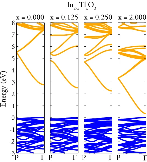
The HSE06 calculated band structures for In2O3,
In1.875Tl0.125O3, In1.75Tl0.25O3, and Tl2O3 are shown in
Figure1. It is immediately obvious that the incorporation of Tl causes the band gap to decrease. This is not unexpected as the band gap of isoelectronic and isostructural Tl2O3is only
0.35 eV, due to in large part to very pronounced relativistic stabilisation of the Tl 6sstates.19The CBM effective masses for In2O3, In1.875Tl0.125O3, In1.75Tl0.25O3, and Tl2O3 were
calculated to be 0.30, 0.29, 0.27, and 0.22me, respectively,
[image:3.612.318.557.472.736.2]indicating that the inclusion of Tl also lowers the effective mass, and should promote higher electron mobility.
FIG. 1. Band structure of In2xTlxO3for x¼0.000, 0.125, 0.250, and 2.000.
Blue and orange denote valence bands and conduction bands. The VBM is set to 0 eV in each case.
A simple band alignment derived from a charge neutrality level (CNL, or branch point energy) approach20 is displayed in Figure 2. This approximate model places the ionization potential of In2O3 at 7.81 eV, which is in good agreement
with recent calculated21and experimental measurements.22It is clear that the incorporation of Tl lowers the position of the CBM relative to the vacuum level, necessarily increasing the distance that the CNL is above the CBM. This result indicates that Tl-doped In2O3should be easier to dopen-type and opens
up the possibility that oxygen vacancies, which are the domi-nant intrinsic defect in In2O3and Tl2O3, might transition from
being relatively deep donors in bulk In2O3(Ref.23) towards
being fully ionized as they are in Tl2O3.
15
As we have now established that Tl incorporation decreases the fundamental band gap of In2O3, it is instructive
to investigate how Tl incorporation affects the optical band gap. Both In2O3 and Tl2O3 possess symmetry disallowed
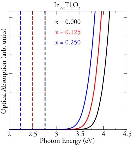
transitions from states within0.8 eV and1.2 eV, respec-tively, of the VBM to the CBM, meaning that their optical band gap is considerably larger than their fundamental band gap. The HSE06 calculated optical absorption spectra for In2O3, In1.875Tl0.125O3, and In1.75Tl0.25O3 are displayed in
Figure 3. Tl-doping up to 12.5% does not affect allowed transitions from VB to CB, meaning that even with a reduced fundamental band gap, the optical band gap remains larger than the threshold for optical transparency of 3.1 eV. This indicates that although the CBM has been lowered, increas-ing the n-type dopability, the doped material is still a TCO.
Very provisional experimental verification of these ideas is provided by the valence band X-ray photoemission spectra shown in Figure4. For nominally undoped In2O3the onset
of the valence band edge is about 2.88 eV below the surface Fermi level, as has been found previously.6,24 The position of the valence band edge is influenced by a number of factors including experimental spectral broadening25and band bend-ing at the surface, leadbend-ing for undoped In2O3to formation of
an electron accumulation layer.7Despite these complications
[image:4.612.317.557.51.248.2]changesin the position of the valence band edge upon alloy-ing with Tl can be regarded as significant. It is therefore interesting to find that the valence band edge moves to lower binding energy with incorporation of Tl, with an onset at 2.49 eV for a surface x value 0.36. Since binding energies are referenced relative to the Fermi energy, which lies close to the CBM, this indicates narrowing of the bandgap in the
FIG. 2. HSE06 calculated optical absorption spectra for In2xTlxO3 for
x¼0.000, 0.125, and 0.250. Dashed lines indicate fundamental band gap, and full lines indicate optical absorption.
FIG. 3. Band alignment of In2xTlxO3 for x¼0.000, 0.125, 0.250, and
2.000 calculated using the CNL alignment method. All energies are given relative to the vacuum level, using the assumption that the CNL sits at
4.5 eV below the vacuum level.20
[image:4.612.327.546.411.725.2] [image:4.612.65.285.495.734.2]surface region probed by XPS assuming that there is no change in the band bending. Somewhat surprisingly however the intensity of the emission from conduction band states close to the Fermi energy decreases slightly with increasing Tl doping. In fact for a sample with nominal bulk composi-tion In1.88Tl0.12O3 it was not possible to locate the Fermi
edge with any confidence. Coupled with the very pronounced surface segregation of Tl found for both samples, these observations suggest that Tl may be partly accommodated at the surface as Tlþ: the propensity of lone pair cations of this sort to segregate to surface sites is well documented.26,27 The Tlþwould effectively act a two electron acceptor, partly compensating the charge carriers arising from oxygen vacan-cies or other native donor defects. Compensation of this sort has been found in Bi-doped PbO2, where Bi acts as an
acceptor rather than as a donor. In the formally related sys-tem Sb-doped SnO2the Sb acts as a donor, as expected from
simple electron counting considerations.27,28Support for the idea of accommodation of a fraction of the Tl in surface sites as Tlþis provided by the observation that the intensity of photoemission in the bandgap region immediately above the extrapolated valence band edge is stronger in the alloy sam-ples than in undoped In2O3: this is where the antibonding
lone pair states are expected.
Overall then it must be acknowledged that even though XPS provides tantalising evidence of bandgap narrowing in In2xTlxO3, the experimental work does highlight obvious
difficulty in incorporating Tl in the bulk of In2O3 and also
suggests that Tl may act to compensate native donors when it segregates to the surface. However the results are suffi-ciently encouraging to warrant investigation of deposition of In2xTlxO3thin films although several safety issues need to
be resolved before we can embark on this work.
Hybrid DFT calculations combined with high resolution XPS measurements have demonstrated that Tl incorporation into In2O3can lead to a significant reduction in the band gap,
arising from pronounced stabilisation of the CBM relative to the vacuum level. Concomitant lowering of the effective mass at the conduction band edge is predicted by the calcula-tions, whilst maintaining optical transparency in the visible region. This effect should in principle make In2O3:Tl a more
efficientn-type TCO even than In2O3. At the same time
low-ering of the CBM relative to the vacuum level will lead to an increase in the work function provided the Fermi level stays close to the CBM, as is found experimentally in the present work. This could lead to improved hole injection in organic light emitting diodes. These issues all warrant further experi-mental investigation, although difficulty in incorporating Tl into the bulk of In2O3may well prove to be problematic.
The work presented here made use of the UCL Legion HPC Facility, the IRIDIS cluster provided by the EPSRC funded Centre for Innovation (EP/K000144/1 and EP/K000136/1), and the HECToR supercomputer through membership of the UK’s HPC Materials Chemistry Consortium, which is funded by EPSRC grant (EP/F067496). The work in Dublin was supported by SFI through the PI programme (PI Grant Nos. 06/IN.1/I92 and 06/IN.1/I92/EC07) and made use of the Kelvin supercom-puter as maintained by TCHPC. X-ray photoelectron
spectroscopy was provided through the EPSRC “Access to Research Equipment Initiative: Cardiff XPS” (Grant No. EP/F019823/1).
1P. D. C. King and T. D. Veal,J. Phys.: Condens. Matter23, 334214 (2011). 2
B. J. Ingram, G. B. Gonzalez, D. R. Kammler, M. I. Bertoni, and T. O. Mason,J. Electroceram.13, 167 (2004).
3
A. Walsh, A. B. Kehoe, D. J. Temple, G. W. Watson, and D. O. Scanlon, Chem. Commun.49, 448 (2013).
4
X. Luo, Y. S. Oh, A. Sirenko, P. Gao, T. A. Tyson, K. Char, and S. W. Cheong,Appl. Phys. Lett.100, 172112 (2012); H. J. Kim, U. Kim, T. H. Kim, J. Kim, H. M. Kim, B. G. Jeon, W. J. Lee, H. S. Mun, K. T. Hong, J. Yu, K. Char, and K. H. Kim,Phys. Rev. B86, 165205 (2012); H. J. Kim, U. Kim, H. M. Kim, T. H. Kim, H. S. Mun, B. G. Jeon, K. T. Hong, W. J. Lee, C. Ju, K. H. Kim, and K. Char, Appl. Phys. Express 5, 061102 (2012); D. O. Scanlon,Phys. Rev. B87, 161201(R) (2013); D. O. Scanlon and G. W. Watson,J. Mater. Chem.22, 25236 (2012).
5
A. Walsh, J. Buckeridge, C. R. A. Catlow, A. J. Jackson, T. W. Keal, M. Miskufova, P. Sherwood, S. A. Shevlin, M. B. Watkins, S. M. Woodley, and A. A. Sokol,Chem. Mater.25, 2924 (2013); S. B. Zhang,J. Phys.: Condens. Matter14, R881 (2002).
6
A. Walsh, J. L. F. Da Silva, S. H. Wei, C. Korber, A. Klein, L. F. J. Piper, A. DeMasi, K. E. Smith, G. Panaccione, P. Torelli, D. J. Payne, A. Bourlange, and R. G. Egdell,Phys. Rev. Lett.100, 167402 (2008). 7P. D. C. King, T. D. Veal, D. J. Payne, A. Bourlange, R. G. Egdell, and
C. F. McConville,Phys. Rev. Lett.101, 116808 (2008). 8
K. H. L. Zhang, V. K. Lazarov, T. D. Veal, F. E. Oropeza, C. F. McConville, R. G. Egdell, and A. Walsh,J. Phys.: Condens. Matter23, 334211 (2011); A. Walsh, C. R. A. Catlow, K. H. L. Zhang, and R. G. Egdell,Phys. Rev. B83, 161202 (2011).
9
D. O. Scanlon and A. Walsh, Appl. Phys. Lett.100, 251911 (2012); N. Feldberg, J. D. Aldous, W. M. Linhart, L. J. Phillips, K. Durose, P. A. Stampe, R. J. Kennedy, D. O. Scanlon, G. Vardar III, R. L. Field, T. Y. Jen, R. S. Goldman, T. D. Veal, and S. M. Durbin,ibid.103, 042109 (2013). 10
M. H. Harunsani, F. E. Oropeza, R. G. Palgrave, and R. G. Egdell,Chem. Mater.22, 1551 (2010).
11G. Kresse and J. Hafner,Phys. Rev. B49, 14251 (1994). 12
G. Kresse and D. Joubert,Phys. Rev. B59, 1758 (1999). 13
A. V. Krukau, O. A. Vydrov, A. F. Izmaylov, and G. E. Scuseria,J. Chem. Phys.125, 224106 (2006).
14M. Burbano, D. O. Scanlon, and G. W. Watson,J. Am. Chem. Soc.133, 15065 (2011); D. O. Scanlon, A. B. Kehoe, G. W. Watson, M. O. Jones, W. I. F. David, D. J. Payne, R. G. Egdell, P. P. Edwards, and A. Walsh, Phys. Rev. Lett.107, 246402 (2011); J. P. Allen, D. O. Scanlon, and G. W. Watson,Phys. Rev. B81, 161103(R) (2010); D. O. Scanlon and G. W. Watson,J. Mater. Chem.21, 3655 (2011).
15
A. B. Kehoe, D. O. Scanlon, and G. W. Watson,Phys. Rev. B83, 233202 (2011).
16P. Agoston, K. Albe, R. M. Nieminen, and M. J. Puska,Phys. Rev. Lett.
103, 245501 (2009). 17
M. Gajdos, K. Hummer, G. Kresse, J. Furthmuller, and F. Bechstedt,Phys. Rev. B73, 045112 (2006).
18B. Adolph, J. Furthmuller, and F. Bechstedt,Phys. Rev. B63, 125108 (2001). 19
P. A. Glans, T. Learmonth, K. E. Smith, J. Guo, A. Walsh, G. W. Watson, F. Terzi, and R. G. Egdell,Phys. Rev. B71, 235109 (2005).
20
A. Schleife, F. Fuchs, C. Rodl, J. Furthmuller, and F. Bechstedt, Appl. Phys. Lett.94, 012104 (2009).
21
A. Walsh and C. R. A. Catlow,J. Mater. Chem.20, 10438 (2010). 22
M. V. Hohmann, P. Agoston, A. Wachau, T. J. M. Bayer, J. Brotz, K. Albe, and A. Klein,J. Phys.: Condens. Matter23, 334203 (2011). 23S. Lany and A. Zunger,Phys. Rev. Lett.106, 069601 (2011). 24
A. Bourlange, D. J. Payne, R. G. Egdell, J. S. Foord, P. P. Edwards, M. O. Jones, A. Schertel, P. J. Dobson, and J. L. Hutchison,Appl. Phys. Lett.92, 092117 (2008).
25P. D. C. King, T. D. Veal, F. Fuchs, C. Y. Wang, D. J. Payne, A. Bourlange, H. L. Zhang, G. R. Bell, V. Cimalla, O. Ambacher, R. G. Egdell, F. Bechstedt, and C. F. McConville,Phys. Rev. B79, 205211 (2009). 26
P. A. Cox, R. G. Egdell, C. Harding, W. R. Patterson, and P. J. Tavener, Surf. Sci.123, 179 (1982); A. Gulino, A. F. Tavener, S. Warren, P. Harris, and R. G. Egdell,Surf. Sci.315, 351 (1994).
27
S. Rothenberg, D. J. Payne, A. Bourlange, and R. G. Egdell,J. Appl. Phys.
102, 113717 (2007).
28P. A. Cox, R. G. Egdell, C. Harding, A. F. Orchard, and W. R. Patterson, Solid State Commun.44, 837 (1982).