I
MODEL
LXS-D SERIES
This manual applies to units
bearing serial no. prefixes A-E
&LAMBDA
INSTRUCTION MANUAL
FOR
REGULATED POWER SUPPLIES
MODEL
LXS-D SERIES
This manual applies to units bearing serial no. prefixes A-E
This manual provides instructions intended for the operation of Lambda power supplies, and is not to be reproduced without the written consent of Lambda Electronics Corp. All information contained herein applies to all LXS-D models unless otherwise specified.
LAM~DA ELECTRONICS CORP. MELVILLE, L.I., N.Y.
TABLE OF CONTENTS
Section
SPECIFICATIONS AND FEATURES
THEORY OF OPERATION
OPERATING INSTRUCTIONS
Basic Mode of Operation
Connections for Operations
Supply Load Connections
Operation After Protective Device Shutdown
MAINTENANCE
General
Trouble Analysis
Checking Transistors and Capacitors
Trouble Chart
Performance Checks
Adjustment of Calibration Control R2
SERVICE
PARTS ORDERING
Page
1
3
3
3
3
4
5
6
6
6
6
7
9
9
9
SPECIFICATIONS AND FEATURES
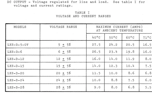
DC OUTPUT - Voltage regulated for line and load. See table I for voltage and current ratings.
TABLE I
VOLTAGE AND CURRENT RANGES
MODELS VOLTAGE RANGE MAXIMUM CURRENT (AMPS)
AT AMBIENT TEMPERATURE
40°C· 50°C 60°C 71°C
LXS-D-5-0V 5
-
+ 5% 27.5 24.2 20.5 16.5LXS-D-6 6
-
+ 5% 26.5 23.4 19.8 16.0LXS-D-12 12
-
+ 5% 16.0 14.0 11.9 8.0LXS-D-15 15
-
+ 5% 14.0 12.3 10.4 7.5LXS-D-20 20
-
+ 5% 11. 5 10.0 8.6 6.8LXS-D-24 24
-
+ 5% 10.0 8. 8 7.5 6.0LXS-D-28 28
-
+ 5% 9.0 8.0 6.8 5.5Current range must be chosen to suit the appropriate maximum ambient temperature. Current ratings apply for entire voltage range.
REGULATED VOLTAGE OUTPUT
Regulation . . . 0.1% line or load with input variations from 105-132 or 132-105 volts AC and load varia-tions from no load to·full load or full load to no load.
Ripple and Noise . . . 1.5 millivolts rms; 5 millivolts peak to peak with either positive or negative terminal
grounded. Temperature
Coefficient . . . Output change in vo~tage 0.03%/oC.
Remote Programming
External Resistor . . . Nominal 1000 ohms/volt output
Programming Voltage . . . . One-to-one voltage change.
Remote Sensing . . . Provision is made for remote sensing to eliminate effect of power output lead re-sistance on DC regulation.
[image:4.624.64.589.70.389.2]AC INPUT - 105-132 VAC at 47-440 Hz. Input Power: 450 Watts*. For operation at 47-53 Hz delete 40°C current rating. For 63-440 Hz consult factory.
*With output loaded to full current rating and input voltag~ 132 volts AC, 60 Hz.
OVERLOAD PROTECTION
Thermal . . . • . . . • • . . • . . Thermostat resets automatically when over-temperature condition is eliminat~d.
Electrical
External . .••...•..• . Automatic electronic current limiting cir-cuit, limits output current to a presetsaf~
value.· Auto~ati~ ~urrent limiting protects the load and power supply when external· overloads and direct shorts occur.
Internal (LXS-D-5-0V,
LXS-D-6 only) . . . . • • . Circuit breaker CBl, provides protection against int~rnal circuit failure.
OVERVOLTAGE PROTECTION - Model LXS-D-5-0V includes a fixed built-in overvoltage protection circuit which prevents damage to the load caused by excessive power supply output voltage. Overvoltage protection firing range is between 6.2' and 7.4 volts D.C.
INPUT AND OUTPUT CONNECTIONS - Terminal blocks on rear of ch~ssis.
OPERATING AMBIENT TEMPERATURE RANGE AND DUTY CYCLE - Continuous duty .from OoC to 71°C ambient.
STORAGE TEMPERATURE (non operat ing)
-VDC Adjust Control - Voltage adjust control permits adjustment of DC output.
PHYSICAL DATA
Size . • . . . • . . 4-15/16" x 7-1/2" x 9-3/8"
Weight . . . 23 Ibs. 'net; 26 Ibs. shipping wt. Finish . . . . • . . • . . . • . • . Gray, FED. STD. 595 No. 26081
MOUNTING - Three surfaces, each with tapped mounting holes can be uti-lized for mounting this unit. All LXS-D power supplies can be mounted with Top, Front, or Left Side facing up. Top, Front, or Left Side must b~ in a horizontal plane. Refer to figure 10 for mounting details.
"V" OPTION - All LXS-D power supplies can be obtained for 205-265 VAC INPUT or 187-242 VAC INPUT. See namepl~te for AC INPUT rating. See schematic diagram for rewiring of AC INPUT. For operation at 47-53Hz, delete 40°C current rating. For 63-440Hz, consult factory.
ACCESSORIES
Rack adapters ...•••.••• Rack adapters LRA-IO, LRA-ll, and LRA-13 used for ruggedized mounting with or without
chassis slides are available.
Overvoltage Protector .. Externally mounted, Overvoltage Protectors LM-OV-l, LM-OV-2, and LM-OV-3 are available .
. Standard Power System .. The LXS-D power supply may be integrated in the Lambda Standard Power System Assembly which provides a pilot light, voltage
cont-rol, fuse, and output metering for the power supply.
THEORY OF OPERATION
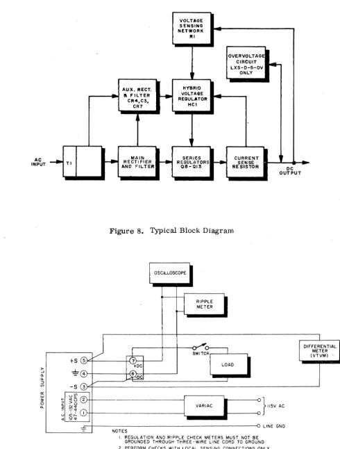
The Lambda power supply consists of an AC input circuit and trans-former; a bias supply consisting of an auxiliary rectifier and filter; and a main regualtor circuit consisting of the main rectifier filter, series regulator transistors, and Hybrid Voltage Regulator. The Hybrid Voltage Regulator (HCl) utilizes thick-film resistors, capacitors, monolithic integrated circuits and power driver transistors in chip form to achieve maximum reliability. The circuit arrangement is shown in block diagram form, Figure 8.
Single phase input power is applied to transformer Tl through terminals land 2.
The main rectifier, a full wave rectifier, provides the power which is filtered by capacitor Cl and then regulated via series regulators Q8-Ql3. Auxiliary rectifiers CR4 and, as applicable, CR7 provide vol-tage filtered by capacitor C3 for regulator control circuits located in HCl.
OV CIRCUIT, FUNCTIONAL DESCRIPTION (LXS-D-5-0V ONLY)
When the power supply output voltage increases above zener break-down voltage of CR9 (approximately 6.2 volts) and gate voltage of SCRl (approximately 0.6 volts), CR9 conducts and current is supplied to the gate of SCRl. SCRl fires causing the power supply output voltage to drop.
OPERATING INSTRUCTIONS
BASIC MODE OF OPERATION
This power supply ope!ates as a constant voltage source provided the load current do~s not exceed the rated value at 40°C. For continuous operation, load current must not exceed the rating for each ambient temperature. When rated load current is exceeded, both voltage and current decrease until voltage reaches zero and the current at short circuit is reduced to a safe value, which is less than the 40°C cutrent rating.
CONNECTIONS FOR OPERATION
Ground Connections. The Lambda power supply can be operated either with negative or positive output terminal grounded. Both positive and negative ground connections are shown in the diagrams for all suggest-ed output connections illustratsuggest-ed in this manual.
Connection Terminals. Make all connections to the supply at the ter-minal block on the rear of the supply. Apply input power to terter-minals 1 and 2; always connect ~he ungrounded (hot) lead to terminal 1.
The supply positive terminal is brought out to terminal
7.
The supply negative terminal is brought out to terminal6.
Recommended wiring of the power supply to the load and selection of wiring isshown in figures 1 through 9. Selection of proper wiring is made on the basis of load requirements. Make all performance checks and mea-surements of current or voltage at the rear output terminals. Connect measuring devices directly to terminals or use the shortest leads possible.
SUPPLY LOAD CONNECTIONS
Connections for Operation as a Constant Voltage Source
The output impedance and regulation of the power supply at the load may change when using the supply as a constant voltage source and con-necting leads of practical length are used. To minimize the effe~t of the output leads on these characteristics, remote sensing is used. Re-commended types of supply-load connections with local or remote sensing are described in the following paragraphs.
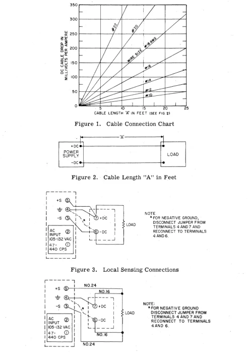
Refer to figure 1 to determine voltage drop for particular cable length, wire size and current conditions. Lead lengths must be measured from supply terminals to load terminals as shown in figure 2.
Two-Wire Connection, Figure
3.
The two-wire connection with local sensing is the connection suitable for applications with relatively constant load.Four-Wire Connection, Figure
4.
The four-wire connection with remotesensing~ provides complete compensation for the DC voltage drops in the connecting cables. Sensing leads should be a twisted pair to minimize AC pick-up. A 2.5 mf elect., capacitor may be required between output terminals and sense terminals to reduce noise pick-up.
Programmed Voltage Connections~ Using External Resistor, Figure
5.
Dis-crete voltage steps can be programmed with a resistance volt~ge divider valued at a nominal 1000 ohms/volt change and a shorting-type switch as shown in figure ,5. When continuous voltage variations are required, use a variable resistor with the same 1000 ohms/volt ratio in place of the resistive voltage divider and short~ng-type switch. Use a low tempera-ture coefficient resistor to assure most stable operation.Before programming, adjust programming resistor for zero resistance and set voltage adjust control to the minimum rated output voltage. Output voltage of programmed supply will nominally be minimum output voltage plus 1 volt per 1000 ohms.
Programmed Voltage Connections Using Programming Voltage, Figure
6.
The power supply voltage output can be programmed with an externally connected programming power supply. The output voltage change of the programmed supply will maintain a one-to-one ratio with the voltage of the programming supply if the output voltage control of the programmed supply is set to minimum output voltage. Output voltage of programmed supply will be minimum output voltage plus voltage of programming
supply.
The programming supply must have a reverse current capability of
1.1 mao minimum.
Alternatively, when supplies with less than 1.1 mao reverse current capability are used, a resistor capable of drawing 1.1 mao at the min-imum programming voltage must be connected across the output terminals of the supply. Th-is programming supply must be rated to handle all excess resistor current at the maximum programming voltage.
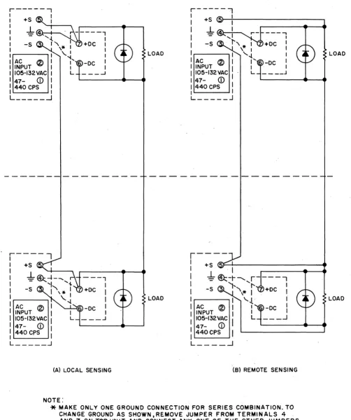
Connections For Series Operation, Figure 7.
The voltage capability of LXS-D power supplies can be extended by series operation. Figure
7
shows the connections for either local or remote sensing in a series connection where the voltage control of each unit functions independently to control the output.A diode, having a current carrying capability equal to or greater than the maximum current rating
of
the supply, must be used and con-. nected as shown in figure 7. The diode blocking voltage should be at least twice the maximum rated output voltage of the supply. See table I of SPECIFICATIONS AND FEATURES for power supply current and voltage ratings.OPERATION AFTER PROTECTIVE DEVICE SHUTDOWN
Thermal Shutdown
The thermostat opens the input circuit only when the temperature of the transistor heat radiator exceeds a maximum safe value. The therm-ostat will automatically reset when the temperature of the heat sink
decreas~s to a safe operating value. After eliminating the cause(s)
for overheating and allowing time for the power supply to cool to a proper temperature, resume operation of the supply.
Overvoltage Shutdown
When the power supply output voltage increases above the overvoltage limit, SCRl will short circuit output of the supply. After eliminating the cause(s) for overvoltage, resume operation of the supply by momen-tarily interrupting the AC input circuit. (refer to TROUBLE SHOOTING CHART)
Circuit Breaker Shutdown (LXS-D-5-0V and LXS-D-6 only)
and power supply will operate in the normal current limiting mode. The circuit breaker will trip when the maximum rated current value for the circuit breaker is exceeded. If CBl trips, check for cause and repair as necessary. To resume operation, place CBI in ON position.
MAINTENANCE
GENERAL
This section describes trouble analysis routine and replacement pro-cedures that are useful for servicing the Lambda LXS-D power supply. A trouble chart is provided as an aid for the troubleshooter. Refer to the section on SPECIFICATIONS AND FEATURES for the minimum performance standards.
,TROUBLE ANALYSIS
Whenever trouble occurs, systematically check primary power lines, external circuit elements, and external wiring for malfunction before trouble shooting th~ equipment. Failures and malfunctions often can be traced to simple causes such as improper jumper and supply-load
connections.
Use the electrical schematic diagram and block diagram, figure
8,
as an aid to locating trouble causes. The schematic diagram contains various circuit voltages that are averages for normal operation~ Mea-sure these voltages using the conditions for meaMea-surement 'specified onth~ schematic diagram. Use measu~ing probes carefully to avoid, causing short circuits and damaging circuit components.
CHECKING TRANSISTORS AND CAPACITORS
Check transistors with an instrument that has a highly limited cur-rent capability. Observe proper polarity to avoid error in meastire-ment. The forward transistor resistance is low but never zero;- back-ward resistance is always higher than the forback-ward resistance.
For good transistors, the forward resistance for any junction is always greater than zero.
Do not assume trouble is eliminated when only one part is replaced. This is especially true when one transistor fails, causing other tran-sistors to fail. Replacing only one transistor and turning power on before checking for additional defective components could damage the replaced component.
When soldering semi-conductor devices, wherever'possible, hold the lead being soldered with a pair of pliers placed between the component and the solder joint to provide an effective heat sink.
TROUBLE CHART
The trouble chart is intended as a guide for locating trouble causes and is used along with the schematic diagram.
The operating conditions assumed for the trouble chart are as follows:
a) AC power of proper voltage and freQuency is preset at input terminals.
b) Either positive or negative terminal is connected to chas sis ground.
c) The power supply is connected for constant voltage with local sensing. See schematic; dotted lines indicate jumpers connected for local sensing operation.
Symptom
1. Zero volts DC output
TROUBLE SHOOTING CHART
Prob able C aus e
Short circuit across out-put of supply.
Open CBl (as applicable).
R5 open, Q5 shorted (as appli cable) .
Open thermostat, Sl.
Series regulator section open.
Current sensing resistor open.
Auxiliary rectifiers CR4, CR7 open (as applicable)
Remedy
Check load and load connections, correct as necessary.
Refer to "Symptoms
3, 4, 5,
an d6."
Check R5 for open, Q5 for short; replace as necessary.
Refer to table I of SPECIFICATIONS AND FEATURES for current ratings at given am-bient temperature. After allowing time for the power supply to cool, resume oper-ation of power supply.
Check HCl pin 10 for correct voltage read-ing (as indicated on schematic diagram).
Check R25-R30 for open, replace as necessary.
Symptom
2. Unable to adjust output volt age.
3. High ripple at line frequency or twice line fre-quency and unreg-ulated DC output.
4.
Same as 3, ex-cept inter-mittent.5. Large spikes at output.
6.
Output voltage too high.7.
Very low out-put voltage on LXS-D-5-0V.TROUBLE·SHOOTING CHART
Probable Cause
Damaged VDC'adjust control.
R2 set too low.
Series regulator sec-tion shorted.
C3 open.
Foreign matter fallen into unit.
Defective rectifiers CRI, CR2 and, as
applicable, CR3, CR5.
RI set too high; open sensing lead.
SCRI fired due to OV condition.
Remedy
Check RI for short or open, replace as necessary.
Refer to ADJUSTMENT OF CALIBRATION CON-TROL R2.
Check Q8-Q13 for short; replace as necessary.
Check C3 for open; replace as required.
Check for loose bench hardware and wire clippings that may have fallen through
cover.
Replace as required.
Check setting of RI; check output connec-tions.
Momentarily interrupt AC input. -If supply operates normally, a transient has occured in line or load, check wiring (switches, etc.) If supply fails to
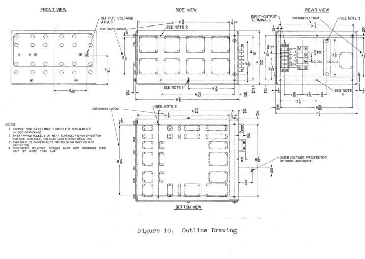
PERFORMANCE CHECKS
Check the ripple and regulation of the power supply using the test connection diagram shown in figure
9.
Use suggested test equipment or equivalent to obtain accurate results. Refer to SPECIFICATIONS AND FEATURES for minimum performance standards.Set the differential meter, DC DVM (John Fluke Model SOlH or equi-valent) to the selected power supply operating voltage. Check the power
supply load regulation accuracy while switching from the load to no-load condition. Long load leads should be a twisted pair to minimize AC pick-up.
Use a Variac to vary the line voltage from 105-132 or 132-105 volts AC and check the power supply line regulation accuracy on the DVM
differential meter.
Use a VTVM, Ballantine 320 or equivalent, to measure rms ripple voltage of the power supply DC output. Use oscilloscope to measure peak-to-peak ripple voltage of the power supply DC output.
ADJUSTMENT OF CALIBRATION CONTROL R2
Whenever QS-Q13, HC1, R25-R30, or R2 are replaced, .and voltage and current indications do not reflect maximum ratings, adjust R2 as
follows. The adjustment procedure requires that the power supply is removed from associated equipment, is at an ambient temperature of 25-30 oC, and is stabilized and not operating.
1. Remov~ AC input power to the supply.
2. Break seal on wiper of R2 from resistor housing and turn to full CW position.
3. Operate power supply for constant voltage with local sensing, connected as shown in figure,3, with no external load.
4. Turn voltage adjust control until minimum rated output voltage is obtained.
5. Apply load so that output current is 110% of 40°C rating for the unit.
6.
Using an oscilloscope, Tektronix 503 or equivalent, observe output voltage while adjustingR2 in CCW direction. Adjust R2 until output ripple increases sharply and oscilloscope pattern changes. .7.
After adjustment is completed, remove AC power input to the supply and use glyptol sealant to seal wiper of R2 to resistor housing.S. After sealing, check setting and repeat adjustment procedure if required.
SERVICE
Please include the power supply model and serial number together with complete details of the problem. On receipt of this information, Lambda will supply service data or advise shipping for factory repair service.
All repa~rs not covered by the warranty will be billed at cost and an estimate forwarded for approval before work is started.
PARTS ORDERING
Standard components and special components used in the Lambda power supply can be obtained from the factory. In case of emergency, criti-cal spare parts are available through any Lambda office.
The following information must be included when ordering parts:
1. Model number and serial number of power supply and purchase date.
2. Lambda part number.
3. Description of part together with circuit designation.
CIRC. DESIG. C1, C2 C3 C4 C5 C6, C7 C8 C9 C10 CB1 CR1, CR2 CR3 CR4 CR5, CR6 CR7 CR8 HC1 Q1 thru Q4 Q5 Q6, Q7 Q8 thru Q13 R1 R2 R3, R4 R5, R7 R8 R9 thru Rll R12 PARTS LIST
The electrical parts located on Lambda models LXS-D-5-0V - LXS-D-28 are listed here. Parts common to a group of models are listed first. Unique parts of individual models within the group are listed separately, by model, immediately following the group common-parts listing. In addition, there are separate listings of parts for the "V" option and LMOV accessory.
COMMON PARTS , COMMON PARTS (Cont.)
MODELS LXS-D-5-0V AND LXS-D-6 MODELS LXS-D-5-0V AND LXS-D-6 (Cont.)
LAMBDA UNIT CIRC. LAMBDA
DESCRIPTION NO. PRICE DESIG. DESCRIPTION NO.
Cap., elect., 60,000 mf CBT-60-036 $10.50 R13 Res., WW, 0.30 ohm DFM-30-053
-10 +100%, 15 vdc .±. 5%, 3w
Cap., elect., 2,100 mf CBS-21-043 3.87 R14 Res., comp., 1,000 ohms DEB-1021
-10 + 100%, 35 vdc ±.10%,'h w
Cap., elect., 3,600 mf CBS-36-044 3.00 R15 Not assigned
-10 + 100%, 20 vdc thru
Cap., mylar, 0.15 mf CGM-15-005 .50 R22
.±. 10%, 200 vdc R23 Res., comp., 33 ohms DEB-3301
Not assigned .±. 10%, 'I. w
Sl Thermostat FKA-155-020
Cap., mylar, 0.033 mf CGL-33-009 .50
.±. 10%, 400 vdc
Cap., mylar, 0.01 mf CGL-10-002 .36
UNIQUE PARTS .±. 10%, 200 vdc
Not assigned MODEL LXS-D-5-0V
Circuit breaker FHC-40-000-2 10.59
Rectifier FBL-00-083 3.57
Cll* Cap., elect., 10 mf CBP-10-027
.±. 20%, 10 vdc
Not assigned CR9 Rectifier, zener diode FBM-Z-140
Rectifier FBL-00-094 .99 R6 Res., comp., 100 ohms DCB-1011
Not assigned .±.10%, % w
SCR1 Rectifier, silicon FBP-00-036
Same as CR4 controlled
Not assigned T1 Transformer ABA-LXS-D-5
Hybrid regulator FBH-24-009 50.00 * Not used on units with serial no. prefix A
Not assigned
Transistor, NPN FBN-LllO 3.25 MODEL LXS-D-6
Not assigned R6 Not assigned
Transistor, NPN FBN-36485 4.13 T1 Transformer ABA-LXS-D-6
COMMON PARTS
Res., var., WW, DNS-22-056 2.50
MODELS LXS-D-12 AND LXS-D-15 2,100 ohms ±. 5%, 2w
Res., Var., WW, DNS-12-087 1.37 C1, Cap., elect., 32,000 mf ·CBT-22-021
1,200 ohms.± 10%, 2w C2 -10+100%,40 vdc
Not assigned C3 Cap., elect., 40 mf CBP-40-014
-7'12 +88'12%, 35 vdc
Res.,comp., 620 ohms DEB-6215 .15 C4 Cap., elect., 2,100 mf CBS-21-043
.±. 5%, Y2W -10 +100%,35 vdc
Not assigned C5 Cap., mylar, 0.15 mf CGM-15-005
Res., center tapped, WW, DFM-20-054 1.50 .±. 10%, 200 vdc
0.2 ohm .±. 5%, 22 W C6 Cap., mylar, 0.1 mf CAM-10-012
.±. 10%, 200 vdc
Not assigned C7 Not assign~d
UNIT PRICE
$ .50
COMMON PARTS (Cant.) COMMON PARTS (Cant.)
MODELS LXS-D-12 AND LXS-D-15 (Cant.) MODELS LXS-D-20 - LXS-D-28 (Cant.)
CIRC. LAMBDA UNIT CIRC. LAMBDA UNIT
DESIG. DESCRIPTION NO. PRICE DESIG. DESCRIPTION NO. PRICE
C8 Cap., mylar, 0.033 mf CGL-33-009 $ .50 C8 Cap., mylar, 0.033 mf CGL-33-009 $ .50
..±.. 10%, 400 vdc ..±.. 10%, 400 vdc
C9 Cap., mylar, 1 mf CBN-10-009 1.33 C9 Not assigned
±"'20%, 3·5 vdc C10 Cap., mylar, 470 pf CGJ-47-002 .32
C10 Cap., mylar, 470 pf CGJ-47-002 .32 ..±.. 10%, 200 vdc
..±.. 10%, 200 vdc Cll, Not assigned
C11, Not assigned C12
C12 C13 Cap., elect., 2 mf CBN-20-024 1.20
C13 Same as C9
CR1 Rectifier FBL-00-083 3.57 -10+50%, 100 vdc
thru C14, Not assigned
CR3 C15
CR4 Rectifier FBL-00-030 1.40 C16 Cap., elect., 10 mf CBP-10-078 1.19
CR5 Same as CR1 -10+50%, 50 vdc
HC1 Hybrid Regulator FBH-24-018 50.00 C17 Not assigned
Q1 Not assigned thru
thru C24
Q7 C25 Same as C6
Q8 Transistor, NPN FBN-36485 4.13 CR1 Rectifier FBL-00-083 3.57
thru thru
Q13 CR3
R1 Res., var., ww, 3,300 DNS-33-057 2.50 CR4 Rectifier FBL-00-030 1.40
ohms..±.. 5%,2 w CR5 Same as CR1
R2 Res., var, ww, 1,200 DNS-12-087 1.37 CR7 Not assigned
..±.. 10%, 2w CR8 Same as CR4
R3, Not assigned HC1 Hybrid regulator FBH-24-010 50.00
R4 Q1 Not assigned
R5* Res., camp., 47 ohms DEB-4701 .12 thru
±. 10%, 1f2 w Q7
R6 Not assigned Q8 Transistor, NPN FBN-36220 2.85
R7 Res., camp., 1,800 ohms DGB-1821 .18 thru
±.10%,lw Q13
R8 Not assigned R2 Res., var., ww, DNR-20-048 1.80
thru 200 ohms, ±. 10%, 2W
R16, R3, Not assigned
R18 R4
thru R5* Res., ww, 1,200 ohms DFS-12-016 .93
R22 ..±..3% 3 w
R23 Res., camp., 33 ohms DEB-3301 .12 R6, Not assigned
"±"10%, 1/2 w R8
R24 Not assigned thru
R25 Res., ww, 0.22 ohm DFM-22-045 1.00 R15
thru ±. 5%, 5w R16 Res., center tapped, ww, DFM-20-054 1.50
R30 0.2 ohm ±. 5%, 22 w
Sl Thermostat FKA-155-020 2.85 R18 Not assigned
* On units with serial no prefixes A & B, R5 is thru
180 ohms, DEB-1811. R22
UNIQUE PARTS R23 ..±.. 10%, Res., camp., 33 ohms 1f2 w DEB-3301 .12
MODEL LXS-D-12 R24 Res., ww, 1,500 ohms DFS-15-045 .70
R17 Not assigned ±.3%, 3 w
T1 Transformer ABA-LXS-D-12 53.67 R25 thru ..±..5%,5w Res., ww, 0.39 ohm DFM-39-046 1.81
MODEL LXS-D-15 R30
R17 Res., film, 2,700 ohms DCS-27-020 .25 Sl Thermogtat FKA-155-020 2.85
±. 5%, 1/2 w * On units with serial no. prefixes A & B, R5 is
T1 Transformer ABA-LXS-D-15 54."21 1,500 ohms, DFS-15-045, $.50
COMMON PARTS UNIQUE PARTS
MODELS LXS-D-20 - LXS-D-28 MODEL LXS-D-20
C3 Cap., elect., 80 mf CBP-80-077 1.62 C1, Cap., elect., 22,000 mf CBT-22-021 12.12
-10 + 75%, 20 vdc C2 -10 + 100%,40 vdc
C4 Cap., elect., 1,100 mf CBS-ll-042 3.67 CR6 Rectifier, zener diode FBM-ZI43 .45
-10 +100%,60 vdc Rl Res., var., ww, 4,500ohms DNS-45-050 3.00
C5 Cap., mylar, 0.15 mf CGM-15-005 .50 ±. 5%, 2w
±. 10%,200 vdc R7 Res., camp., 2,200 DGB-2221 .12
C6 Cap., mylar, 0.1 mf CAM-I0-012 .65 ohms..±.. 10%, 1 w
..±..10 %,200 vdc R17 Not assigned
C7 Not assigned Tl Transformer ABA-LXS-D-20 54.06
UNIQUE PARTS (Cont.) PARTS FOR OVERVOLTAGE ACCESSORY MODELS
MODEL LXS-D-24 LMOV-1, LMOV-2, LMOV-3 (Cont.)
COMMON PARTS (Cont.)
CIRC. LAMBDA UNIT CIRC. LAMBDA UNIT
DESIG. DESCRIPTION NO. PRICE DESIG. DESCRIPTION NO. PRICE
C1. Cap., elect., 13,000 mf CBT-13-023 $ 12.39 R3 Res., film, 200 ohms DCR-20-010 $ .20
C2 -10 + 100%, 60 vdc .±. 5%, Y. w
CR6 Rectifier, zener diode FBM-Z143 .45 R4 Res., thermistor, DKR-43-004 1.52
R1 Res., var., WW, DNS-90-058 2.75 425 ohms,.±. 5%,1 Iii W
9,000 ohms.±. 5%, 2 W R5, Res., comp., 1,200 DEB-1221 .12
R7 Res., comp., 2,200 ohms DGB-2221 .12. R6 ohms.±. 10%, 'h w
.±.10%, 1 w R8 Res., comp., 15,000 DEB-1531 .12
R17 Not assigned . ohms.±. 10%, 'h w
T1 Transformer ABA-LXS-D-24 53.04 RIO Same as R5
SCR1 Rectifier, silicon FBP-00-009 6.00
MODEL LXS-D-28 controlled
C1, Cap'., elect., 13,000 mf CBT-13-023 12.39
C2 -10 +100%,60 vdc UNIQUE PARTS
CR6 Rectifier, zener diode FBM-ZI44 .81
MODEL LMOV-1
R1 Res., var., WW, DNS-90-058 2.75
9,000 ohms.±. 5%, 2 W Q2 Transistor, PNP FBN-L103 1.50
R7 Res., comp., 2,700 ohms DGB-2721 .09 R1 Res., var., WW, DNS-20-034 3.00
.±.10%, 1 W 2,000 ohms.±. 10%, 1 W
R17 Res., film, 5,100 ohms DCS-51-002 .25 R2 Res., film, 560 ohms DCR-56·002 .65
.±. 5%, 'h W .±. 2%, 'h W
T1 Transformer ABA-LXS-D-28 53.91 R7 Res., comp., 33 ohms DCB-3305 .15
.±. 5%, % W
PARTS FOR "V" OPTION R9 Not assigned
On all LXS-D models with suffix "V",
MODEL LMOV-2 capacitor C8 and transformer T1 change.
Part no .. change for C8 is listed here. For Q2 Transistor, PNP FBN-L103 1.50
transformer T1 used on these models, Rl Res., var., WW, DNS-50·036 3.15
see standard LXS-D model parts list 5,000 ohms.±. 10%, 1 W
for the standard transformer part no. R2 Res., film, 1,470 ohms DCS-15-031 .30
and add suffix "G"* to the part no. Price .±.1 %, 'h W
for T1 does not change R7 Res., comp., 33 ohms DCB-3305 .15
* Suffix "V" on units with serial no. prefixes .±. 5%, % W
A-C. R9 Not assigned
ALL MODELS MODEL LMOV-3
C8 Cap., paper, 0.01 mf CAL-10-021 1.77 Q2 Transistor, PNP FBN-L114 3.50
.±.10%, 1000 vdc R1 Res., var., WW, DNT-20-010 2.85
PARTS FOR OVERVOLTAGE ACCESSORY MODELS R2 Res., film, 4,700 ohms 20,000 ohms,.±. 10%, 1 W DCS-47-028 .30
LMOV-1, LMOV-2, LMOV-3 .±. 2%, 'h W
COMMON PARTS R7 .±. 5%, % Res., comp., 39 ohms DCB-3905 .15
W
C1 Cap., mylar, 0,01 mf CGL-10-008 .50 R9 Res., comp., 22 ohms DEB-2201 .12
.±. 20%, 80 vdc .±. 10%, 'h W
Q1 Transistor, NPN FBN-:L102 2.40
350r---~---~,_----,_~,__,---~
300r---+---A---¥---1----~~
~ 250r---+---,~~--~--+---~---~
~~ Oo~
0<1
a: a: 200 r---+-f---¥---;
Ow wOo .J(/)
~lb 15 0 r---tl----+---I---j.<'----+----7""'-t---~
u~
g:J
.J [image:17.615.58.551.22.723.2]~ 100r---~~--~~~~~--+---~~----~
Figure
1.
Cable Connection Chart
. I ''AI ~I
-!-DC POWER
LOAD SUPPLY
-DC
Figure 2. Cable Length "A" in Feet
,---,
I
+S I
..J....
-S
AC I
INPUT I
105-132 VAC I
47-
CD
I440 CPS I L--.-_----'
I
L _ _ _ _ _ -.J- - - - I
I
I
I I
I
LOAD
NOTE
*
FOR NEGATIVE GROUND, DISCONNECT JUMPER FROM TERMINALS4 AND 7 AND RECONNECT TO TERMINALS 4 AND6.Figure 3. Local Sensing Connections
,---,
I I NO.24
+S " i } - - - - , - - - ,
I NO.16
I ..J....
I 'I,
I -S 3 1"\
*
II I \ I I ''j-..
I AC M\
I INPUT 1.61 I I I 105-132 VAC I ~ I 47-
CD:
: 440 CPS
I
L _ _ _ _ _ -.J NO.24
LOAD
NOTE:
*
FOR NEGATIV E GROUND DISCONNECT JUMPER FROM TERMINALS 4 AND 7 AND RECONNECT TO TERMINALS 4AND 6.r - - - 1.----I-LJV\N-J\NvLllJ\NJ\Nv~
I
i"S I
I
-S
AC I
INPUT I 105-132 VAC : 47- CD I 440 CPS
I
L _ _ _ _ _ ..J-
----,
I
I
I
I I
LOAD
NOTE;
=
-S
AC ® I
INPUT I 105-132 VAC : 47- CD I
440 CPS
I
L _ _ _ _ _ ..J*
FOR NEGATIVE GROUND, DISCONNECT JUMPER FROM TERMINALS 4 AND 7 AND(A) LOCAL SENSING RECONNECT TO TERMINALS (B) REMOTE SENSING 4AND6
Figure 5. Programmed Voltage,with External Resistor
PROGRAMMING PROGRAMMING
VOLTAGE VOLTAGE
r-~:-f
'I,
I'
-S
.---_ _ ---, I
AC
®
IINPUT 1 105-132 VAC : 47- CD 1 440 CPS
I
L _ _ _ _ _ ..J
r---~
i"S
G5 :
-.l I
_
4~r--'--S 'I,
1
'*
\ I ILOAD
NOTE:
AC ® I
INPUT I 105-132 VAC : 47- CD I
440 CPS
I
L _ _ _ _ _ ..J*
FOR NEGATIVE GROUND, DISCONNECT JUMPERFROM TERMINALS 4 AND 7 AND RECONNECT
'i--I
I
L.... _ _ _ .-I
(A) LOCAL SENSING TO TERINALS 4 AND 6. (B) REMOTE SENSING
Figure 6. Programmed Voltage, with External
Programming Voltage Source
LOAD
[image:18.612.61.556.68.757.2]r---,
+S I I
---,
... -1.. I
-S
,"'\*:
+DC :.---~ I \., I I AC , " . . . . , INPUT (Z) 1 : 6 -DC I 105-132VAC 1 L _ _ _ ...J 47-
<D
I440 CPS I
'---' I
L _____ ~
+S
AC
®
IINPUT I
105-132 VAC I 47-
<D
I440 CPS I
L _____ ..J
---,
1+DC I
I
1
1 I
L.. _ _ _ oJ
(A) LOCAL SENSING
LOAD
LOAD
r---,
+S ~~I---~
1
..L
(4)...;I----...,..I
-S t'\ I
\* I
.---~ 1 '-t AC (Z) I I ....
INPUT I I
- - - - , I +DC I I
I
-DC I
I _ _ _ _ J
105-132 VAC I L..
47-
<D
L...-_ _ _ ... _ ... 440 CPS :L.. _ _ _ _ _ J
r----1 +S I . I
I
-!-
@):;:-t--..r- -- -.,
I
'1..."
II -S
",*
I +DC I.I I " 1 r 1
I ... 1
AC
®
I I, -DC 1I INPUT I
I '05-132VAC
I
L - - _...147-
<D
L...-_ _ _ ... _ _ ~: 440CPS
I
L _ _ _ _ ...J,
(8) REMOTE SENSING
NOTE: .
*
MAKE ONLY ONE GROUND CONNECTION FOR SERIES COMBINATION. TO CHANGE GROUND AS SHOWN,RE.MOVE JUMPER FROM TERMINALS 4 AND 7 ON TOP UNIT AND CONNECT ANY ONE OF THE OTHER JUMPERSAS SHOWN IN DOTTED LINE. - - - .'
Figure 7. Series Connection
LOAD
[image:19.613.54.556.40.640.2]AC INPUT
>-.J
a. a.
:::>
U>
a:
w
3
o
a.
---.
TI+5 5
~4
-5
CD
lOU>
:; e;2
~~
- <t (i)
" I <{),..
Q<t
~
VOLTAGE SENSING NETWORK
ftl
OVERVOLTAGE CIRCUIT
f4-LXS-D-5-0V
•
ONLYAUX. RECT. HYBRID 8 FILTER
r--
VOLTAGE--CR4,C3, REGULATOR
CR7 HCI
,
I---
RECTIFIER MAINr--
REGULATORS SERIESr--
CURRENT SENSE --AND FILTER Q8-Q13 RE SISTOR DCOUTPUT
Figure 8. Typical Block Diagram
I
OSCILLOSCOPERIPPLE METER
~
~
SWITCH I+DC LOAD
~
I
VARIACI
:}115VAC LINE GND NOTESI. REGULATION AND RIPPLE CHECK METERS MUST NOT BE GROUNDED THROUGH THREE·WIRE LINE CORD TO GROUND 2 PERFORM CHECKS WITH LOCAL SENSING CONNECTIONS ONLY
I DIFFERENTIAL
[image:20.621.66.557.60.706.2]METER (VTVM)
FRONT VIEW
I
0 0 0
I 0 0
0 0 0 0 0
® ®® ®
0 0 0 0 0
0 0 0 0 0
® ®
~3..L,~ 64
/
0
f
0
0
ADJ
CUSTO
1
I
"6
']
SIDE VIEW REAR VIEW
t
I
SEE NOTE II I 4 3 2 J-7 J i'--L
13
I
is n + 14 I "-SEE NOTE - J..si--o • 611. I--~ 64 64 8 1--1.!.§1,-'-II.9. -1--!2- 2 8
~ 64 64 32 16 16
1---~9
t
3 * - - - - 1CUSTOMERS CUTOUT
---t
EE NOTE 2 621 :--~ . ~ ~ 64 ;ll 664 33.. , ,!---~ 3 64 7 64 l!. 7-2' ---~
NOTES
I. PROVIDE 5/16 DIA. CLEARANCE HOLES FOR SCREW HEADS ON SIDE OF PACKAGE.
2. 8-32 TAPPED HOLES, 6 ON REAR SURFACE,4 EACH ON BOTTOM AND SIDE SURFACES, FOR CUSTOMER CHASSIS MOUNTING, 3.' TWO NO. 6-32 TAPPEO HOLES FOR MOUNTING OVERVOlTAGE
PROTECTOR.
4. CUSTOMERS MOUNTING SCREWS MUST NOT PROTRUDE INTO UNIT BY MORE THAN 3/B ':
6~
- - - - \ - I - 8e
p-"-o .0'0 , I
bd
Q .. --.d
F'l
P1
h,J
bd
Figure 10.
g,'
,.:a'"
g:': '
',:JjI
'0 ( J ' - ' ' ' O ~"-"Cl
b o._ .. ->J
~~~:~
I:(L,~,..d
P-"--'l
6..._,_d
BOTTOM VIEW
Outline Drawing
OVERVOLTAGE PROTECTOR
[image:21.796.42.759.53.561.2]Q9 THRU QI3 R9B THRU RIIB 0.1 FBN-364B5 IIW WW ,_ _ _ _ _ _ _ _ _ _ "..,;i}.ii,:. _____ ,
A21 /'<12.9V) I 12.BV I FBN-36485 Q8 R9A 1 I
I
L
A23
CR7 CR4 FBL-00-094 FBL-OO
094
~--~--~~~--+-~~----~----~~~ 0.1 IVDCI 5.0V
AS R23 Ae IIW, WW (6.0V)
r=..:....:c*"4>---.A9 33 .-_----,R2 (NOTE 7)
RI3 0.3
H-""VVIr-" 3W WW RI4 IK C9 0.01 200V MYLAR 1.2K 2W
WW RI 2.2K :!:IO% 2W WW 1 CR9 FBM-ZI40 (NOTE II)
+V
25.4V All
C2 + (24.4V) ~~~~t.L~to""~---'"'t---1f'---~~
C4 3600
20V + FBL-00-083
(NOTE 7) Ale 10 II ELECT. C5 0.15 200V MYLAR 60,000 15V ELECT (2)
AI9 HCI SCRI.~"f--"
FBP-00-036
NOTES:
C3 2,100 +
35V ELECT.
I. RESISTORS ARE COMP. 1/2W WITH VALUES IN OHMS, UNLESS OTHERWISE NOTED.
2. RESISTOR TOLERANCES: COMPo ±IO%, FILM ±I%, WIREWOUND ±5%, UNLESS OTHERWISE NOTED. 3. CAPACITOR VALUES ARE IN MICROFARADS. 4. CAPACITOR TOLERANCES: MYLAR ±IO%,
ELECTROLYTIC -10 +100%.
5. DESIGNATIONS ARE LAMBDA PART NUMBERS. 6. SYMBOLS:
t INDICATES CLOCKWISE ROTATION OF SHAFT.
~ INDICATES CONNECTION TO CHASSIS.
- INDICATES TERM. ON PRINTED CIRCUIT BOARD. DINDICATES ACTUAL UNIT MARKING.
7. CONDITIONS FOR CIRCUIT POINT MEASUREMENTS: INPUT: 115VAC, 60Hz. RATED VOLTAGE NO LOAD. INDICATED VOLTAGES ARE TYPICAL VALUES AND ARE D.C. UNLESS OTHERWISE NOTED, D. C. MEASUREMENTS TAKEN WITH 20,000 OHMS/V VOLTMETER BETWEEN -V (TERM.4) AND INDICATED POINTS UNLESS OTHERWISE NOTED. VOLTAGES IN PARENTHESIS APPLY ONLY TO MODEL LXS-D-6. A SINGLE
R7 620 ±5%
FBH-24-009
IB 16
'-4.6v
AI4
B. FOR 47-53Hz DELETE 40°C CURRENT RATING FOR 63-440 Hz INPUT, CONSULT FACTORY. 9. COAT MOUNTING SURFACE OF QBTHRU QI3
WITH DOW CORNING NO. 340 SILICONE GREASE.
(NOTE III
SI
10. CB IS O.OIMF,±IO%,IOOOV, PAPER ON UNITS WITH "V" OPTION.
II. ON MODEL LXS-D-6, R6, SCRI,CR9 AND CII ARE NOT USED.
12. CII NOT USED ON SERIAL NO. PREFIX A.
13. ON UNITS WITH "V" OPTION, TI HAS TAPPED PRIMARY. "V" OpTION UNITS CAN BE WIRED FOR
IB7-242V INPUT (USING TAP), OR
R6 100
1/4W
(NOTE III
CB 0.033 400V MYLAR
O.OV
-v
-S
} 105-132 VAC 47-440 Hz (NOTES 8 a 13)
SCHEMATIC DIAGRAM REGULATED POWER SUPPLY
FOR 205- 265V (US I NG EN TI RE 'F--O=-R"""'-'W=-I R=-I=-N=-G=-O=-F=-=-PO--W-E=-R--SU=-P--P--L.:--Y--=T=-O:-1 PRIMARY). ON SERIAL NO.
PREFIXES A-C, "V" OPTION UNITSj LOAD REFER TO SUPPLY-TO-LOAD TI PRIMARY IS NOT TAPPED. AC WIRING DIAGRAMS.
INPUT IS 205-265V. DOTTED CONNECTIONS SHOWN ON 14. ON UNITS WITH SERIAL NO TBI INDICATE JUMPERS IN PLACE PREFIXES A-D A TERMINAL FOR LOCAL SENSING CONNECTION. BOARD IS USEblN PLACE OF THE
P. C. BOARD.
THIS SCHEMATIC APPLIES TO UNITS BEARING SERIAL NO. PREFIXES A - E
&.LA~BDA
E LECTROtiIiCS. CORP. MELVILLE, NEW YORK
Q9 THRU QI3 R26 THRU R30 FBN-36220 5~~~W (NOTE 7)
r---Q--- - --
-'II\IIr--l
C I I I
(NaTE 15) T ,-"1"""" __ .... ________ ... ~~~
__
£--.-.~__
~ ~__
~:______
~__
-+~R~2~5 __ -4I~ ____ ~ ________ ~~~ ____ ~ ____ --HI 0.39 +V
I
I
L
!
)EI
~~3 5W, WWR7 2.2K IW (NOTE II -..---+---. RI 9K :!:5% RI7 2W 5.1K,5% WW
16T"-'-I~:=---~2t-;l--~.-l--:--~F~IL~M~~ (NOTE 12)
(NOTE
II)
AllAIS 20 FBH-24-010 HCI
C4 1,100 60V ELECT.
C5 +
0.15 200V MYLAR
+
A22~ __ 1~6 ____________ ~1~8 __ ~IIj-I1~L-::~--~ R2 R24 1.5K±3% 3W,WW CI3 2,I00V -10+50% ELECT. NOTES:
I. RESISTORS ARE COMPo 1/2W WITH VALUES IN OHMS, UNLESS OTHERWISE NOTED.
2. RESISTOR TOLERANCES: COMPo ±IO%, FILM ±I%, WIREWOUND ±5%, UNLESS OTHERWISE NOTED. 3. CAPACITOR VALUES ARE IN MICROFARADS. 4. CAPACITOR TOLERANCES: MYLAR £10%,
ELECTROLYTIC -10 +100%.
5. DESIGNATIONS ARE LAMBDA PART NUMBERS .. 6. SYMBOLS:
t INDICATES CLOCKWISE ROTATION OF SHAFT.
~ INDICATES CONNECTION TO CHASSIS.
-&-INDICATES TERMINAL ON PRINTED CIRCUIT BOARD. DINDICATES ACTUAL UNIT MARKING.
7. CONDITIONS FOR CIRCUIT POINT MEASUREMENTS: INPUT: 115VAC, 60Hz. RATED VOLTAGE NO LOAD. INDICATED VOLTAGES ARE TYPICAL VALUES AND ARE D.C. UNLESS OTHERWISE NOTED, D. C. MEASUREMENTS TAKEN WITH 20,000 OHMS/V . VOLTMETER BETWEEN -V (TERM.4) AND INDICATED POINTS UNLESS OTHERWISE NOTED. SEE TABLE I FOR VOLTAGE VALUES. AIO +C1610 50\1,-10+50% ELECT. 200,2W WW RI6 0.05,22W, WW
8. FOR 47-53Hz DELETE 40°C CURRENT RATING FOR 63-440 Hz INPUT~ CONSULT FACTORY. 9. COAT MOUNTING SURFACE OF Q8 THRU QI3
WITH DOW CORNING NO. 340 SILICONE GREASE. C8 0.033, 400V
MYLAR (NOTE 10)
10. C8 IS O.OIMF±IO%,IOOOV, PAPER ON UNITS WITH "V" OPTION.
II. ON MODEL LXS-D-28 R7 IS 2.7K. RI7 IS REPLACED BY A JUMPER ON LXS-D-20,-24.
12. ON MODEL. LXS-D-20 RI IS 4.5K, CI AND C2 ARE. 22,000 MFD, 40V.
13. ON UNITS BEARING SERIAL NO. PREFIXES A 8 B R5 IS 1.5K.
14. ON MODEL LXS-D-28, CR6 IS FBM-ZI44.
15. ON UNITS WITH 'V' OPTION, TI HAS TAPPED PRIMARY."V"·OPTION UNITS CAN BE WIRED FOR 187-242V INPUT (USING TAP), OR
FOR 205-265V (USI~!l ENTIRE PRIMARY). ON SERIAL NO. PREFIXES A-C, V· OPTION UNITS; TI PRIMARY IS
NOT TAPPED. AC INPUT IS 205-265'1. r:F='=O='=R.:..cW"'-I='=R""IN"':G-=-O-=-F=-=P-=-OW=ER=-=S""'UP::":P=-=-t.:""'y-:"f::"::O"'" 16. ON UNITS WITH SERIAL NO. PREFIXES
A-D, A TERMINAL BOARD IS USED IN PLACE -OF THE' P. C. BOARD.
LOAD REFER TO SUPPLY-TO-LOAD WIRING DIAGRAMS.
DOTTED CONNECTIONS SHOWN ON TBI I NDICATE JUMPERS IN PLACE FOR LOCAL SENSING CONNECTION.
(O.OV) O.OV
-V
} 105-132 VAC 47-440 Hz (NOTES 8 815)
TABLE I
SCHEMATIC VOLTAGE VALUES MODEL (VAe) A I(V~) VDC) (VOC) C 0
LXS-D-20 26 15 35 40 LXS-D-24 32 15 42 43 LXS-D-28 36 15 48 47
SCHEMATIC DIAGRAM REGULATED POWER SUPPLY
MODELS LXS-D-20 LXS-D~24 LXS-D-28 E (VDC) 32 34 35 F (veC) 20.3 24.2 28.3
I
THIS SCHEMATIC APPLIES TO UNITSI
BEARING SERIAL NO. PREFIXES A-E&LA:M:DDA
ELECTRONICS CORP. MELVILLE, NEW YORK
Q9 THRU QI3 R26 THRU R30 FBN-364B5 5?;l~w
(NO
JgV7)
r---<Jr--- - --
--'VV'o.---l
(29V)
W
I(NOTE 14) TI (NOTE 7) r-~~--~~~~--~ h--~:~~--~---+~~--~~~--+---~~----~~~~ / I I R25 I
+V
I
1
I I I
L I
I I I BVAC I I
1
I I II I 5V
I
I (21.4Vl" A22 20 I
I 6.6VAC (NOTE : (6.2VAC)
•
7)•
I
~ AI
NOTES:
R7 I.BK
AI4
I. RESISTORS ARE COMPo 1/2W WITH VALUES IN OHMS, UNLESS OTHERWISE NOTED.
2. RESISTOR TOLERANCES: COMPo ±IO%, FILM ±I%, WIREWOUND ±5%, UNLESS OTHERWISE NOTED. 3. CAPACITOR VALUES ARE IN MICROFARADS. 4. CAPACITOR TOLERANCES: MYLAR ±IO%,
ELECTROLYTIC -10 +100%.
5. DESIGNATIONS ARE LAMBDA PART NUMBERS. 6. SYMBOLS:
t
INDICATES CLOCKWISE ROTATION OF SHAFT.~ INDICATES CONNECTION TO CHASSIS.
-&-INDICATES TERMINAL ON PRINTED CIRCUIT BOARD. DINDICATES ACTUAL UNIT MARKING.
7. CONDITIONS FOR CIRCUIT POINT MEASUREMENTS: INPUT: 115VAC, 60Hz. RATED VOLTAGE NO LOAD. INDICATED VOLTAGES ARE TYPICAL VALUES AND ARE D.C. UNLESS OTHERWISE NOTED, D. C. MEASUREMENTS TAKEN WITH 20,000 OHMS IV VOLTMETER BETWEEN -V (TERM.4) AND INDICATED POINTS UNLESS OTHERWISE NOTED. VOLTAGES IN PARENTHESIS APPLY TO MODEL LXS-D-15.
I 0.22 12.0V
I R23 5W,WW (l5.0V)
__ -I 33 (NOTE 7)
IVDC I
16 R2 1.2K 2W WW C9 1 ... 35V
<:0% AI2
~",--t---i I-'+--e-..
~i~ TANT. AI3 10 II
HCI 12 FBH-24-018
IB 14 A2 A3
CIO
i'bCffJ
yl--_ _ --...JMYLAR
RI7 2.7K,5%
FILM (NOTE II)
8. FOR 47-53Hz DELETE 40°C CURRENT RATING FOR 63-440 Hz INPUT, CONSULT FACTORY. 9. COAT MOUNTING SURFACE OF Q8 THRU QI3
WITH DOW CORNING NO. 340 SILICONE GREASE. RI 3.3K :!:5% 2W WW (NOTE 12)
All
SI
C4 + 2)00
35V ELECT.
+ C5 +
0.15 200V MYLAR CI3 1,35V 20% TANT. CB 0.033 400V MYLAR (O.OV) O.OV -V -S
} 105-132 VAC 47-440 Hz (NOTES 8 a 14)
10. CBIS O.OIMF±IO%,IOOOV,PAPERONUNITSWITH"V"OPTION.
II.. RI7 IS REPLACED BY A JUMPER ON MODEL LXS-D-12. 12. ON .MODEL LXS-D-15, RI IS 9K.
13. ON UNITS BEARING SERIAL NO. PREFIXES A a B R5 IS IBO.
SCHEMATIC DIAGRAM REGULATED POWER SUPPLY
14. ON UNITS WITH "v" OPTION, T I ,HAS TAPPED PRIMARY. "V"OPTION UNITS CAN BE WI RED FOR
IB7-242V INPUT (USING TAP), r-FO-R-W-IR_I_N_G_O_F-po_W-ER-S_UP_P-L.:_Y_T_O---' OR FOR 205-265V
(USING ENTIRE PRIMARY). ON LOAD REFER TO SUPPLY-TO-LOAD WIRING DIAGRAMS.
SERIAL NO. PREFIXES A-C, "V" DOTTED CONNECTIONS SHOWN ON OPTION UNITS; TI PRIMARY IS NOT TBI INDICATE JUMPERS IN PLACE TAPPED. AC INPUT IS 205-265V. FOR LOCAL SENSING CONNECTION. 15. ON UNITS WITH SERIAL NO.
PREFIXES A-D, A TERMINAL BOARD IS USED IN PLACE OF THE P.C.BOARD.
~TH~I~S~S~C~H~E~M"AT~IAC~A~P~P~L~IE~S~T~O~UN~I~TS~-' BEARING SERIAL NO. PREFIXES A-E
£LA:M:BDA
ELECTRONICS CORP. MELVILLE, NEW YORK
We warrant each instrument manufactured by us, and sold by us or our authorized agents, to be free from defects in material and workmanship, and that it will perform within applicable specifications for a period of five years after original shipment. Our obligation under this guarantee is limited to repairing or replacing any instrument or part thereof, (except tubes and fuses) which shall, within five years after delivery to the original purchaser, be returned to us with transportation charges prepaid, prove after our examination to be thus defective.
We reserve the right to discontinue instruments without notice, and to make modifications in design at any time without incurring any obligation to make such modifications to instruments previously sold.
LAMBDA
E L E e T RON I e s c 0 R P. 515 BROAD HOLLOW ROAD. MELVILLE, L. I., NEW YORK· 516 MYRTLE 4-4200A
(v'~
SUBSIDIARY