486
ACKNOWLEDGEMENTS
CP/M is a registered trademark of Digital Research, Inc.
XENIX is a trademark of Microsoft Inc.
UNIX is a trademark of Bell Laboratories
FEDERAL COMMUNICATIIONS COMMISSION NOTICE
WARNING
This equipment generates, uses and can radiate radio frequency energy and, if not installed and used in accordance with the instructions manual, may cause interference to radio communications.
It has been tested and found to comply with the limits for a Class A computing device pursuant to Subpart J of Part 15 of FCC Rules, which are designed to provide reasonable protection against such interference when operated in a commercial environment.
About This Manual
This manual is written for a system programmer or analyst
PAGE 1-1 1-1 1-3 1-3 1-3 1-3 1-4 1-4 2-1 2-1 2-3 2-5 2-7 3-1 3-1 3-1 3-4 4-1 4-1 4-1 4-1 4-3 4-3 4-4 4-4 4-4 4-4 5-1 5-1 5-1 5-3 5-3 5-4 5-6 5-7 5-12 5-13 5-23 5-24 5-24 SUBJECT
1. SY~EII OVERVIEW
FEATURES AND CAPABILITIES SYSTEM SOFTWARE
OPERATING SYSTEMS SYSTEM MONITOR DIAGNOSTICS OPI'IONS
RELATED DOCUMENTS
2. SPECIFICATIONS
SYSTEM SPECIFICATIONS POWER SU PPL Y
FLOPPY DISK DRIVE HARD DISK DRIVE
3. SYSTEM ARCBITEC'roRE INTRODUCTION
BUS STRUCTURE MEMORY ARBITRATION
Contents
4. GENERAL SYSTEM FUNcrIONAL DESCRIPrION
INTRODUCTION CPU BOARD
80186 MICROPROCESSOR MEMORY DEVICES
MEMORY MANAGEMENT UNIT (MMU) FLOPPY DISK DRIVE
WORKNET
Z-80A I/O PROCESSOR HARD DISK CONTROLLER BOARD
5. SUBSYSTEM FUNCTIONS
INTRODUCT ION
CENTRAL PROCESSING UNIT (CPU) HARDWARE OVERVIEW 80186 MICROPROCESSOR ARCHITECTURE
Addressing Modes
Direct Memory Access (DMA) Operation Programmable Timer Operation
Interrupt Control Operation MEMORY ADDRESSING
MEMORY MANAGEMENT UNIT SYSTEM CONTROL PORT
TABLE OF CONrEftS
PAGE SUBJECT
5-25 Z-80A I/O CONTROLLER 5-25 Functional Description 5-26 Z-80A I/O Processor Memory 5-27 80186/Z-80A Comrnunnications 5-28 Host/Controller Communication 5-28 Controller Initialization 5-29 Channel Initialization 5-29 Channel Transmit Operation 5-29 Channel TTY Receive Operation
5-29 Channel Ring Buffered Receive Operation 5-30 Modem Status Operation
5-30 REGISTER DEFINITIONS
5-30 Initialization Register 5-31 Control Registers
5-32 Communication Channel Registers 5-36 HARD DISK CONTROLLER HARDWARE OVERVIEW 5-36 INTRODUCTION
5-36 FUNCTIONAL DESCRIPTION 5-36 Disk Drive Description 5-36 Head Selection
5-39 Formatting Guidelines 6-1 6. FIRMWARE IN'rERFACB 6-1 INTRODUCTION
6-1 SYSTEM MONITOR 6-3 Monitor Location 6-4 Debugger Program
6-5 Entering the Debugger Program
6-5 Executing a Debugger Command (An example) 6-12 486 Monitor's System Call Interface 6-18 Power-up Test
6-19 Power-up Test Error Reporting Scheme 6-19 Power-up Test Descriptions
A-I APPENDIX A. 486 CPU JUMPlCR:mG SPECIFICATIONS
B-1 APPENDIX B. PORT CONNECTIONS
ILLUS'l'RATIONS
1-2 Figure 1-1 Altos Model 486 Computer System 3-2 Figure 3-1 Bus Architecture
4-2 Figure 4-1 System Block Diagram 5-2 Figure 5-1 CPU Board Block Diagram
5-8 Figure 5-2 Master/Slave PIC Configuration 5-9 Figure 5-3 Interrupt Request
5-37 Figure 5-4 Hard Disk Controller Board Circuitry 5-40 Figure 5-5 Sector Format
PAGE SUBJECT 5-5 5-5 5-6 5-8 5-10 5-11 5-12 5-13 5-14 5-22 5-23 5-23 5-24 5-25 5-25 5-25 5-26 5-26 5-26 5-28 5-40 5-41 6-3 6-4 6-6 6-13 6-16 6-17 6-18
Table 5-1 Table 5-2 Table 5-3 Table 5-4 Table 5-5 Table 5-6 Tabl e 5-7 Table 5-8 Table 5-9 Table 5-10 Table 5-11 Table 5-12 Table 5-13 Table 5-14 Table 5-15 Table 5-16 Table 5-17 Table 5-18 Table 5-19 Table 5-20 Table 5-21 Table 5-22 Table 6-1 Table 6-2 Table 6-3 Table 6-4 Table 6-5 Table 6-6 Table 6-7
TABLE OF CONrEftS
TABLES
Chip Select Register Offsets DMA Register Offsets
Timer Control Register Offsets
Interrupt Controller Register Offsets System Maskable Interrupts
Master PIC Register Offsets
80186 Microprocessor Predefined Types and Default Priority
System Memory Map
Memory Management Relocation Register Violation Port Bits
Control Port Address Offsets Control Bits
PIA Port Address Offsets
Floppy Disk Control Port Address Offsets Floppy Disk Controller Port Address Off sets
Z80 Port Assignments SIOA Port Address Offsets SlOB Port Address Offsets
Z-8~A Memory Addressing
Internal Hard Disk Connectors Disk Data Format
Conversion from Byte Offset to Sector Number
Monitor Memory Map
Debugger Support Commands Debugger's Command Syntax Monitor System Calls
System Overview
1
PAGE SUBJECT
1-1 FEATURES AND CAPABILITIES 1-3 SYSTEM SOFTWARE
1-3 Operating Systems
1-3 XENIX
1-3 Concurrent CP/M 1-3 System Monitor 1-3 Diagnostics
1-4 OPTIONS
1-4 RELATED DOCUMENTS
ILLUSTRATIONS
FEA~RES AND CAPABILITIES
The Altos 486 is a general purpose l6-bit microcomputer system with a 1 Mbyte floppy disk and 20 Mbyte hard disk storage
capacity in a desktop design. See Figure 1-1. The 486 supports up to four users and a serial printer. The WorkNet port lets you network the 486 system with up to 30 other Altos computer systems
(such as the 186, 586/986, 586T/986T, and the 68000).
The 486 combines the low cost data sharing and communications capability of an intelligent terminal with the computer power necessary to tackle sophisticated business and scientific
problems. The adjustable, low-glare CRT offers a high-resolution display. The adjustable, low-profile keyboard offers 105 keys in the format of a dedicated word processor.
The 486 system provides the following features:
o The Intel 80186 microprocessor with expanded instruction set, built-in direct memory access channels and an interrupt controller and operates at 8Mhz.
o Z-80A I/O processor for high speed data transfer.
o 512 Kbytes of standard main memory; expandable to 896 Kbytes.
o 5-1/4 inch, double-sided, double density floppy disks with 1 Mbyte storage capacity.
o Network communications using the WorkNet interface.
o Five RS232 serial ports.
o Optional 20 Mbyte add-on hard disk for a total of 40 Mbytes of hard disk storage capacity.
SYSTEM SOFTWARE
The 486 uses several software programs to help run the system. These are the operating system, utilities, diagnostics, and the monitor programs. Applications and languages are not discussed in this manual.
OPERATING SYSTEMS
The 486 system supports two multiuser operating systems: XENIX and Concurrent CP/M. These are described below.
XENIX Operating System
This multiuser system complements a large number of applications such as office automation, database management, and communica-tions. It is the Microsoft l6-bit microcomputer implementation of the UNIX operating system developed by Bell Laboratories.
The XENIX operating system supports program development and many software applications. XENIX features a hierarchial file system, compatibility between file, device, and interprocess I/O,
asynchronous processing, a command language interpreter, a large number of subsystems and utilities, excellent file security, user-friendly menus, flexible memory use and compatiblity with a large number of high level languages.
Concurrent CP/M Operating System
Concurrent CP/M (Control Program for Microprocessors) is a multiuser operating system for l6-bit microcomputers. CP/M pro-vides record and file locking with password protection for use in business settings where data base integrity is essential. CP/M also features extensive error handling and reporting, real-time capabilities, and data and time stamps and files.
SYSTEM MONITOR
The system monitor programs and modules reside permanently in the PROMs of the 486 and provide initial system checks and exercise initial coordination and control of the system. The Monitor includes an extensive set of power-up tests used to identify hardware faults in the system, and a debugger program to help find problems in users' programs.
DIAGNOSTICS
The diagnostics programs for the 486 are contained in a separate diskette supplied with the system. These SDX (system diagnostics executive) programs help you isolate problems in system
OPTIONS
Listed below are the options for the 486 System which are available through upgrade kits (U/K).
o An additional 384 Kbytes of RAM for a total of 896 Kbytes of main memory.
NOTE
The standard system is configured with 512 Kbytes of memory. 256 Kbytes are on the CPU board and the other 256 Kbytes are on a pair of memory boards (128 Kbytes each). The memory upgrade kit provides a 512 Kbyte board which is then exchanged with one of the
existing 128 Kbyte memory boards.
o An optional 20 Mbyte add-on hard disk drive unit. RELATED DOCUMENTS
The following Altos publications on the Model 486 Computer System may be referenced to supplement your overall
understanding.
690-15889-001 Setting Up Your 486 Workstation 690-15927-001 Altos 486 SOX Diagnostic Manual 690-15683-001 486 Maintenance Manual
690-15998-001 486 Illustrated Parts List Manual
The Setting Up and Diagnostic Manuals are shipped with the
system. The Maintenance Manual and Illustrated Parts List Manual can be purchased.
Specifications
2
PAGE SUBJECT
2-1 SYSTEM SPECIFICATIONS 2-1 DESCRIPTION
2-1 Rear Panel Connectors and Controls
2-2 POWER REQUIREMENTS 2-2 AC Power
2-2 Heat Dissipation
2-2 CPU OVERALL DIMENSIONS 2-2 ENVIRONMENTAL REQUIREMENTS 2-2 Ambient Temperature
2-2 Relative humidity
2-3 SPECIFICATIONS 2-3 Microprocessor
2-3 Memory
2-3 OTHER SYSTEM SPECIFICATIONS 2-3 POWER SUPPLY SPECIFICATIONS 2-5 FLOPPY DISK DRIVE
2-5 POWER REQUIREMENTS 2-5 DC Power
2-5 Heat Dissipation
2-5 OVERALL DIMENSIONS
2-5 ENVIRONMENTAL REQUIREMENTS 2-5 Operating Temperature
2-5 Non-operating Temperature
2-6 PERFORMANCE SPECIFICATIONS 2-7 HARD DISK DRIVE
2-7 POWER REQUIREMENTS 2-7 DC Power
2-7 AC Power
2-7 Heat Dissipation
2-7 OVERALL DIMENSIONS
2-7 ENVIRONMENTAL REQUIREMENTS 2-7 Operating Temperature
2-7 Non-operating Temperature
SYSTEM SPECIFICATIONS
The following specifications describe the overall dimensions, power, environmental, and performance requirements for the 486 Computer System.
DESCRIPTION
Central Processor (CPU) Floppy Disk Drive Hard Disk Drive WorkNet
Rear Panel Connectors and Controls
AC Power ON/OFF Switch AC Power Input Receptacle AC Fuse Holder
System Reset Button
WorkNet is a local area network capable of supporting up to 30 other Altos computers.
Serial RS232 Ports support asynchronous terminals and printers.
POWER REQUIREMENTS
AC Power
Volts Hertz
Amperes (Maximum) Fuse Type
Fuse Size
Heat Dissipation
Watts
BTU per/Hour
CPU OVERALL DIMENSIONS
Height (inches) Width (inches) Length (inches)
115 60 3
4A - 250V 3AG 180 614 230 50 2
2A - 250V 3AG
Weight (Free standing weight) (pounds)
3.5 17 15 20
ENVIRONMENTAL REQUIREMENTS
To ensure best performance from the 486 System, avoid extremes in temperature or humidity. These conditions are likely causes of floppy and hard disk drive malfunctions. For further information about environmental constraints, refer to the ENVIRONMENTAL
REQUIREMENTS for specific components. It is recommended that you position the 486 System so that disk drives are maintained in a horizontal position.
o 0
Ambient Temperature 59 to 90 F (15 to 32 C)
Relative Humidity 20 to 80 (percent) Temperature
(Maximum wet bulb Non-condensing
Degree Farenheit) 78
MICROPROCESSOR>
Intel - ae186
Address/Data Bus (bits) Processor Speed (Megahertz) DMA Channels
Programmable Interrupt Controller Programmable l6-bit Timers
Zilog - zae
Address Bus (bits) Data Bus (bi ts)
Processor Speed (Megahertz)
MEMORY
Standard Maximum
OTHER SYSTEM SPECIFICATIONS
Electrostatic Discharge Dissipation 10 KV (with no hard errors) 3eePf
Agency Approvals
FCC, Class A, UL, CSA Designed to meet VDE, lEe
PCMER SUPPLY SPECIFICATIONS
o Output Voltages and Maximum Rated Loads
Output 1: +5.ev at 15.0 A
1 16
a
2
1 3
1 16 8 4
512 Kbytes 896 KBytes
Output 2: +12 V at 4.e A (surging to 7 A for Ie sec to start disk)
Output 3: -12 V at e.5 A
Continuous Output Power is 153 watts
0 Overall Regulation (from all causes)
Output 1: ± 3% max at 75% load ± 25% load change Output 2: ± 5% max at 6e% load ± 40% load change Output 3: ± 5% max at 6e% load ± 4e% load change
0 Noise and Ripple
o Input Voltage (at all rated load conditions)
u.s.:
95 VAC to 130 VAC single phaseEurope: 190 VAC to 260 VAC single phase
o Efficiency at maximum continuous output power and nominal line input:
70% min; forced air cooling available, approximately 30 cfm.
o Overvoltage protection threshold Output 1: 6.25 V ± 0.75 V
o Temperature Range
o to 50 degrees C ambient
o Mean Time Between Failures 20,000 hours (continuous)
o Safety and Emissions Requirements UL and CSA mandatory
VDE approvable
FLOPPY DISK DRIVE POWER REQUIREMENTS DC Power
Volts
Amperes (typical) Volts
Amperes (typical Seeking) Heat Dissipation
Watts OVERALL (Except Height Width Length (Front Height Width
Continuous Seek (typical) Standby (typical)
Motor off (typical)
DIMENSIONS
for front panel) (inches) (inches) ( inches) Panel) (inches) (inches)
Total overall Weight (pounds)
ENVIRONMENTAL REQUIREMENTS
+5.0 0.6 +12.0 0.7 11.4 9.0 5.6 1.62 5.75 8.0 1.65 5.83 2.9
o 0
Operating Temperature 41 to 109.4 F (5 to 43 C) Relative humidity
(percent non-condensing)
(Maximum wet bulb temperature)
20 to 80 850F (290C)
o
Non-operating Temperature -4 to 125 F (-20 to
o
PERFORMANCE SPECIFICATIONS
Memory capacity
Unformatted
Number of:
Disk (Megabytes) Track (Kilobytes)
Double Density
1 6.25
Cylinders
sa
Head/Cylinder 2
Total Tracks (S0 per side) 160
Transfer Rate (Kilobits/sec) 250
Rotational Latency (milliseconds average) 100
Access Time
Track to Track (ms) Average (ms)
Motor Starting Time (ms) Settling Time (ms)
Head loading Time (ms)
Encoding Method Index
Rotational Speed (rpm)
Disk Diameter (inches)
Track Density (Tracks per inches)
2-6
3 94 250 15 50
MFM
1
300
5.250
HARD DISK DRIVE
POWER REQUIREMENTS
DC Power
Volts
Steady State: (percent) Amperes (typical)
(Maximum)
Ripple (Maximum percent allowed with equivalent resistive load) Start Surge: (Maximum percent)
Amperes (Maximum) (10 Seconds typical)
Volts (±5 percent) Amperes (typical)
(Maximum)
Ripple (Maximum percent allowed with equivalent resistive load)
AC Power
None required
Heat Dissipation
watts (typical) (Maximum)
OVERALL DIMENSIONS
Height (inches) Width (inches) Length (inches) Weight (pounds)
ENVIRONMENTAL REQUIREMENTS
+12 ±5 1 1.2 1 ±10 2.5 +5 0.4 0.5 2 14 17 1.63 5.88 8.0 4.5
o 0
Operating Temperature 40 to 122 F (4 to 50 C)
Relative humidity
(percent non-condensing) 8 to 80 (Maximum wet bulb temperature) 780F (26oC)
o 0
Non-operating Temperature -40 to 135 F (-40 to 57 C)
PERFORMANCE SPECIFICATIONS Memory Capacity:
Unformatted
Drive (Megabytes) Surface (Megabytes) Track (Kilobytes) Cylinder (Kilobytes) Formatted
Number of:
Drive (Megabytes) Surface (Megabytes) Track (Kilobytes) Sector (bytes) Sector/track
Cylinders Head/Cylinder Data Tracks Surfaces Disks
Transfer rate (Megabits/sec.) Access Time
25.5 6.38 10.416 41.664 20 10 8 512 16 612 4 2448 4 2 5.0
Average Latency (ms) 8.33 Seek Time (including settling time)
Single Track (ms) 15
Average (ms) 85
Maximum (ms) 190
Rotational Speed (rpm) Recording Density
Areal (TPI x BPI) (Mbi ts/sq. in. ) Linear (MFM)
Radial (Tracks per inch) Disk Diameter (inches)
PAGE SUBJECT 3-1 INTRODUCTION 3-1 BUS STRUCTURE
System Architecture
3
3-4 MEMORY ARBITRATION
ILLUSTRATIONS
INTRODUCTION
This chapter describes the architecture of the 486 Computer System through a discussion of the bus structure and memory arbitration unit.
BUS STRUCTURE
The CPU is made up of various physical data and address buses that determine the general architecture of the system. Refer to Figure 3-1.
The major buses are the XLA Bus, MP (Mapped Address) Bus, AD (Address) Bus, BD (Buffered Data) Bus, ZD~-7 Bus, LA (Logical Address) Bus, MD Bus,and Z8~ Address Bus.
The AD bus is a multiplexed 16-bit address/data bus from the
w
I
to.)
245
lS373
186
GRANT
20
XlA 12-19
lS245
14
16
BO BUS
I I
8
o
MAP
2148
lS 245
16
16
LS245
I/O
DEVICES
Figure 3-1
XlA BUS
MAIN MEMORY
MO BUS
XLAO
CENTRAL ARBITER
16
LS 245
Bus Architecture
ZOO-07
The 8~186 requires a 2~-bit address to access all the possible locations in main memory; a 16-bit address can only access 65,536 bytes of memory. The processor creates this 2~-bit address by appending four low order zeros (A0 through A3) to the 16-bit segment address (which specifies a 64K segment of memory) and combining this with a 16-bit offset address (which specifies a location within the segment). This 2~-bit bus is called the logical address (LA) bus.
The LA Bus is created from the AD Bus when the addresses are 1 atched at ALE time and hel d for the entire bus cycl e. The boot and diagnostic PROM are addressed via the LA bus. When the LA bus is buffered, the XLA bus is developed.
The XLA bus provides virtual memory capability through relocation registers residing between the bus and the main memory. This means that if the data ,during a DMA transfer, is not in physical memory location it will be transferred into memory from the disk by the relocation registers addressing space process.
The CPU board design is divided into two major hardware sections, the 8~186 section and the Z80 section. The XLA Bus connects these two major sections together so that either processor can access the main memory.
The BD Bus is within the 8~186 section, it is the (Buffered) Bus which is created from the multiplexed AD Bus. The BD Bus is an I/O bus. All devices which are in the I/O space of the 80186 processor send and receive data on this bus.
The Mapped Address Bus is created through the Memory Management Unit (MMU). One function of the MMU is to create page addressing to memory. Another function of the Memory Management Unit is to protect the operating system from normal user access.
Within the Z8~ section is the ZD~-7 (Data) Bus which is used by the Z80 Microprocessor to transfer eight data bits from the SIO ports to main memory and the 186 through the MD (Memory Data bus) •
MEMORY ARBITRATION
These are all the buses for the 486 system. You will note that both the Z8~ and 8~186 processors require main memory access. To allow both the Z8~ and 8~186 buses to share main memory, a cen-tral arbitration unit is used. This arbitration unit controls access to main memory.
The central arbitration unit is a three way arbiter - arbitrating requests between the 186 and Z8~ and a refresh cycle. When a memory cycle has been allowed access to the bus, that
request will be the only one serviced on the bus. A requesting memory cycle cannot interrupt a currently executing cycle.
A refresh cycle must take place at lease every 15.6 us to
PAGE SUBJECT 4-1 INTRODUCTION 4-1 CPU BOARD
General System
4
Functional Description
4-1 80186 Microprocessor 4-3 Memory Devices
4-3 Memory Management Unit (MMU) 4-4 Floppy Disk Drive
4-4 WorkNet
4-4 Z-80A I/O Processor 4-4 HARD DISK CONTROLLER BOARD
ILLUSTRATION
INTRODU C'l' ION
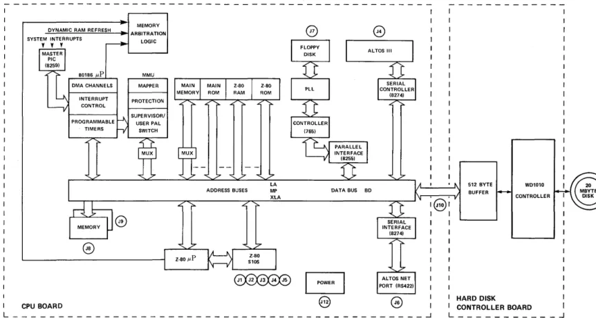
This chapter provides a general description of the 486 system. Figure 4-1 shows a block diagram of the main subsystems which make up the 486. These include the CPU board and the hard disk
controller board which are briefly described below.
CPU BOARD
The CPU board is a multi-functional subsystem that contains the main processor, the I/O processor, the floppy disk drive
controller, 256 Kbytes of main memory, the memory management unit, the memory arbitration logic and the I/O ports for all peripheral interfacing.
8~186 MICROPROCESSOR
The 486 Computer System is designed around the Intel 80186
•
IN
L_
MEMORY DYNAMIC RAM REFRESH .1 ARBITRATION
LOGIC
o
CPU BOARD
0)
~
c=:J
e
Figure 4-1 Syste. Block Diagraa
G
_ _ -1512 BYTE BUFFER
WD1010
CONTROLLER
HARD DISK
CONTROLLER BOARD
The basic features of the 8~186 Microprocessor are as follows: o 16-bit address/data bus
o 8 Mhz clock
o Two independent DMA channels o Programmable Interrupt Controller o Programmable 16-bit timers
In addition, it can address up to I megabyte of memory in banks of 64 Kbytes and over 65,~~~ I/O ports. The CPU performs 8 and 16-bit arithmetic functions in binary or decimal.
The 8~186's internal programmable interrupt control (PIC) acts as a slave to the master external PIC. It is through this
master/slave setup that the microprocessor services system and internal inter r upt s.
The two DMA (Direct Memory Access) channels handle requests from the disk drives and WorkNet port. One channel is for the hard and floppy disks DMA requests; the other is for networking.
MEMORY DEVICES
The system provides four separate memory components to handle the various memory requirements of the system. These are the "main" memory, the system PROM, Z-8~A RAM, and z-8~A ROM.
The standard main memory contains 512 Kbytes of dynamic RAM which is upgradeable to 896 Kbytes. 256 Kbytes are on the CPU board; the remainder are on two memory cards. The PROM contains the power-up tests, the debugger and various boot device drivers. The Z-8~A processing circuitry has 4K of ROM and 2K of RAM for
I/O. The ROM contains the control program and the static RAM performs temporary storage and data buffering.
MEMORY MANAGEMENT UNIT (MMU)
The MMU creates page memory addressing and contains a mapper and protection circuitry. The MMU circuitry is also responsible for switching the system between user and the protected supervisor mode. In user mode, the system executes the shell or application
programs, such as a word processing or an accounting program, for example. In the supervisor mode, monitor programs can be run.
In addition, I/O operations can only take place in the supervisor mode, and for operating systems like XENIX, the kernel must run
FLOPPY DISK DRIVE
The floppy disk circuitry is controlled through the 765 chip and interrupts the microprocessor via the 8255 parallel interface port. Control and read/write signals to and from the disk drive are handled through connector J7 on the CPU. The PLL (Phase Lock Loop) aids the 765 in recovering MFM (Modified Frequency
Modulation) data.
WORKNET
WorkNet enables the 486 to be connected to a network of other Altos computers using synchronous data link control (SDLC). WorkNet conforms to an RS422 electrical standard.
To implement WorkNet, the 486 systems dedicates one of its two DMA channels for this function. A circuit then generates 800 KHz for the network baud rate.
Z-80A I/O PROCESSOR
The Z-80A I/O processor runs a control program that resides in a PROM that is local to the Z-80A. It also uses a small amount of static RAM for temporary storage and buffering. The I/O
processor communicates with the central processor via system memory locations and interrupts. It supports five RS232 channels.
The Z-80A 64K of memory space is divided into two halves. The upper 32K is mapped into the system memory and the lower 32K is mapped into the local PROM and static RAM. The Z-80A can access
the full 512 Kbytes of memory but must do so in blocks of 32 Kbytes each.
BARD DISI COJrmOLLER BOARD
The other major subsystem of the 486 is the Hard Disk Controller unit. The main component on the board is the WD10l0 Winchester chip. The WD10l0 Winchester drive controller chip controls the Hard Disk Drive. Read/write instructions from the
micro-processor enter the Hard Disk Controller board through the J10 connector. The command is then sent to the WD10l0 Controller which controls and monitors a 512 byte buffer used to hold read or write data. One hard disk sector 512 bytes of information. Data is transferred to and from the 20 Mbyte disk drive.
Subsystem Functions
5
PAGE SUBJECT 5-1 INTRODUCTION
5-1 CENTRAL PROCESSING UNIT (CPU) HARDWARE OVERVIEW 5-3 8~186 MICROPROCESSOR ARCHITECTURE
5-3 Addressing Modes
5-4 Direct Memory Access (DMA) Operation 5-6 Programmable Timer Operation
5-7 Interrupt Control Operation 5-12 MEMORY ADDRESSING
5-13 MEMORY MANAGEMENT UNIT 5-23 SYSTEM CONTROL PORT
5-24 FLOPPY DISK CONTROLLER OPERATION 5-24 Programming
5-25 Z-8~A I/O CONTROLLER 5-25 Functional Description 5-26 Z-8~A I/O Processor Memory 5-27 8~186/Z-8~A Communnications 5-28 Host/Controller Communication 5-28 Controller Initialization 5-29 Channel Initialization 5-29 Channel Transmit Operation 5-29 Channel TTY Receive Operation
5-29 Channel Ring Buffered Receive Operation 5-3~ Modern Status Operation
5-3~ REGISTER DEFINITIONS
5-3~ Initialization Register 5-31 Control Registers
5-32 Communication Channel Registers 5-36 HARD DISK CONTROLLER HARDWARE OVERVIEW 5-36 INTRODUCTION
5-36 FUNCTIONAL DESCRIPTION 5-36 Disk Drive Description 5-36 Head Selection
ILLUSTRATIONS
PAGE SUBJECT
5-2 Figure 5-1 CPU Board Block Diagram
5-8 Figure 5-2 Master/Slave PIC Configuration 5-9 Figure 5-3 Interrupt Request
5-37 Figure 5-4 Hard Disk Controller Board Circuitry 5-4~ Figure 5-5 Sector Format
5-5 5-5 5-6 5-8 5-1~ 5-11 5-12 5-13 5-14 5-22 5-23 5-23 5-24 5-25 5-25 5-25 5-26 5-26 5-26 5-28 5-4~
Table 5-1 Table 5-2 Table 5-3 Table 5-4 Table 5-5 Table 5-6 Table 5-7 Table 5-8 Table 5-9 Table 5-1~
Table 5-11 Table 5-12 Table 5-13 Table 5-14 Table 5-15 Table 5-16 Table 5-17 Table 5-18 Table 5-19 Table 5-2~ Table 5-21
TABLES
Chip Select Register Offsets DMA Register Offsets
Timer Control Register Offsets
Interrupt Controller Register Offsets System Maskable Interrupts
Master PIC Register Offsets
8~186 Microprocessor Predefined Types and Default Priority
System Memory Map
Memory Management Relocation Register Violation Port Bits
Control Por t Regi ster Off se ts Control Bits
PIA Port Address Offsets
Floppy Disk Control Register Offsets Floppy Disk Controller Register Offsets
Z8~ Port Assignments SIOA Regi ster Off se ts SlOB Register Offsets Z-8~A Memory Addressing
ItnRODUClION
This chapter discusses the subsystem functions of the 486 system that are of interest to a system programmer. First an overview of the function is provided, then any programmable characteris-tics are discussed followed by addressing and register informa-tion for that funcinforma-tion. As identified in the previous chapter, the main subsystems of the 486 are the CPU board and the Hard Disk Controller board.
CEftRAL PROCESSIS UNIT (CPU) HARDWARE OVERVIEW
The Central Processing Unit (CPU) printed circuit board performs most of the major functions for the 486 system. Refer to Figure 5-1.
The CPU printed circuit board is designed around two major sections of hardware, the 80186 section and the Z-80A section. Within the 186 section are the 186 microprocessor, the floppy disk controller, the boot ROM, the main memory, the memory management unit, the parallel interface controller (8255), and
U1 I N
BD BUS
16 LA BUS
16
A AD
80186
~LS245
16 14 D A
ROM
12
EXPANSION ~
MEMORY
Figure 5-1
.' ---r"---'
Jl J2
CPO Board Block Diagraa
16
Z-80 ADDRESS BUS
The Z-8~A section contains an intelligent serial I/O controller circuitry that provides high speed data transfer to and from the user terminals. Within the Z-8~A section is the Z-8~A micro-processor, three Z-8~A SIO controllers for five channels, two timer devices and a small amount of RAM and ROM.
8~186 MICROPROCESSOR ARCHITECTURE
This section describes the architecture of the 8~186 microproces-sor within the 486 system, specifically the addressing modes, the OMA function and programmable timers.
Addressing Modes
There are three addressing schemes done through the 8~186 in the 486 system: 1) operand addressing, 2) external port or register addressing, and 3) main memory addressing. Memory addressing is discussed later in this chapter.
Operand Addressing
The 8~186 Microprocessor has eight operand addressing modes. Two addressing modes are provided for instructions that operate on internal register or immediate operands and six addressing modes are provided to specify the location of an operand in a memory segment.
A memory operand address consists of two 16-bit components: a segment base and an offset. The segment base is supplied by a 16-bit segment register either implicity chosen by the addressing mode or explicitly chosen by a segment override prefix. The offset is calculated by summing any combination of the following three address elements.
The displacement (an 8- or 16-bit immediate value contained in the instruction)
The base (contents of either the BX or BP base registers) The index (contents of either the SI or 01 index registers)
For more information on operand addressing modes, refer to the data book.
Port and Register Addressing
To obtain the physical address for a port or an external
register, the offset address is added to the base address. The base address refers to a particular address range in the I/O space. For example, if the base address were programmed to start at 1000 and if the floppy status register were being addressed, the offset address, 280 (hex), would be added to the base address, and the result would be 1280 (hex).
NOTE
The default base address in this system is 1000.
The starting address is defined by the PACS register of the 80186 as programmed by the user. For more information on programming the PACS register, refer to the data book.
Pheripheral chip select lines, PCS0* through PCS3*, on the 80186 chip are used to select this starting address range block in the I/O space, PCS0* enables block 1000, PCS1* enables block 2000 and so forth. See the internal PCS register offsets in Table 5-1. An MPCS register determines the mode of operation of the
peripheral chip selects. Refer to the data book for more information on this function.
NOTE
Do not confuse a register or port address offset with a memory offset. A memory offset is used to construct the 20 bit address. Refer to discussions on Bus Structure in Chapter 3 and Memory Addressing later in this chapter.
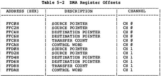
Direct Memory Access (DMA) Operation
Direct Memory Access (DMA) can be instructed, by the Hard Disk Drive Controller printed circuit board, the Floppy Disk Drive Controller chip or the WorkNet, to access the full contents of main memory. Data can be transferred directly from memory to
I/O, memory to memory, or I/O to I/O, without the intervention of the microprocessor. This leaves the mircroprocessor free for other tasks.
The 80186 microprocessor provides two independent high-speed DMA channels. Each channel has six registers in the control block that define that channel's specific operation, see Table 5-1. The control registers consist of a bit source pointer, a 20-bit destination pointer, a 16-20-bit transfer counter and a 16-20-bit control word. Data may be transferred in eight bit or sixteen bit transfers.
Data transfers may be either source or destination synchronized, that is, either the source of the data or the destination of the data may request the data transfer. In addition, DMA transfers may be unsynchronized, that is, transfers take place continually until the correct number of transfers has occurred.
To perform a DMA channel transfer, the channel program provides information that describes the operation by loading values into channel registers. DMA cycles can run in either Supervisor or User state and must be permitted to run without triggering access protection mechanism.
Table 5-1 Chip Select Register Offset
1
ADDRESS (HEX)1
DESCRIPTION1
1---1---1
1
A0H1
UPPER MEM CS1
1
A2H1
LOWER MEM CS1
1
A4H1
PACS REGISTER1
1
A6H1
MID RANGE MEM CS1
1
A8H1
MPCS REGISTER1
1
1
1
Table 5-2 DMA Register Offsets
ADDRESS (HEX) DESCRIPTION 1 CHANNEL 1
FFC0H FFC2H FFC4H FFC6H FFC8H FFCAH FFD0H FFD2H FFD4H FFD6H FFD8H FFDAH
---1---1
SOURCE POINTER SOURCE POINTER DESTINATION POINTER DESTINATION POINTER TRANSFER COUNT CONTROL WORD SOURCE POINTER SOURCE POINTER DESTINATION POINTER DESTINATION POINTER TRANSFER COUNT CONTROL WORD
1 1
1 CH 0 1 1 CH 0 1 1 CH 0 1 1 CH 0 1 1 CH 0 1 1 CH 0 1 1 CH 1 1 1 CH 1 1 1 CH 1 1 1 CH 1 1 1 CH 1 1 1 CH 1 1
Programmable Timer Operation
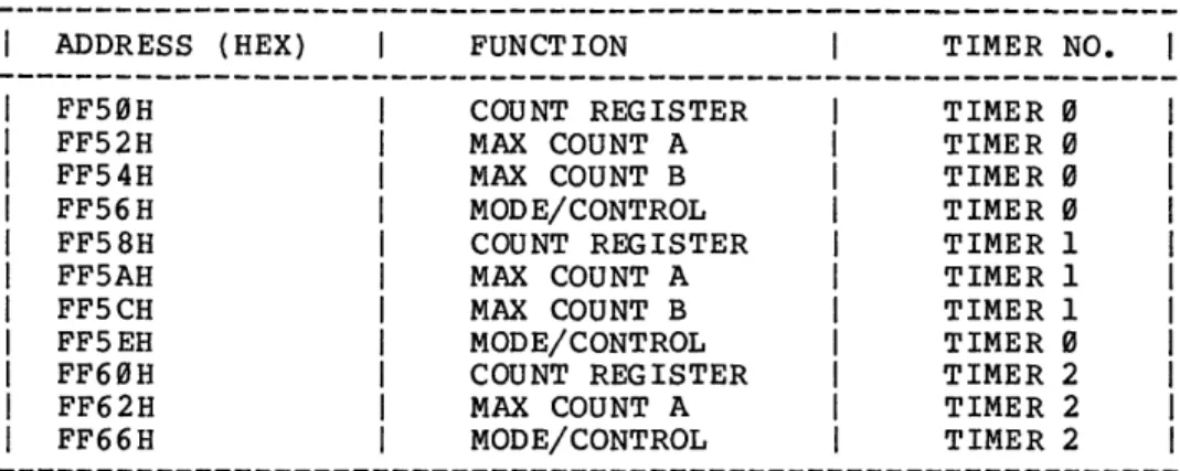
There are three internal l6-bit programmable timers in the 8~186 microprocessor, although only two are pinned out. The other timer is for real time applications and generating delayed
signals. One of the two pinned out timers is used for generating a baud clock signal at 1.2288 Mhz. The other pinned out timer is used for the system clock.
The timers are controlled by eleven l6-bit registers in the internal peripheral control block, see Table 5-3. The count register contains the current value of the timer. It can be read or written at any time independent of whether the timer is run-ning or not. The value of the register will be incremented for each timer event. Each of the timers is equipped with a MAX COUNT register, which defines the maximum count the timer will reach. After reaching the MAX COUNT register value, the timer count value will reset to zero during that same clock, i.e., the maximum count value is never stored in the count register itself. The timers have several programmable options:
o All three timers can be set tc halt or continue on a terminal count.
o Timers ~ and 1 can select between internal and external clocks, alternate between MAX COUNT registers and be set to retrigger on external events.
o The timers may be programmed to cause an interrupt on terminal count.
Table 5-3 Timer Control Register Offsets
ADDRESS (HEX)
FF5~H FF52H FF54H FF56H FF58H FF5AH FF5CH FF5EH FF6~H FF62H FF66H FUNCTION
COUNT REGISTER MAX COUNT A MAX COUNT B MOD E/ CONTROL COUNT REGISTER MAX COUNT A MAX COUNT B MODE/CONTROL COUNT REG ISTER MAX COUNT A MODE/CONTROL
5-6
TIMER NO. TIMER ~
TIMER ~
TIMER ~
TIMER ~
TIMER 1 TIMER 1 TIMER 1 TIMER ~
Interrupt Control Operation
Internal and external interrupts provide a means of stopping the normal processing flow in order to handle unexpected or difficult situations.
The system operates in the RMX Mode and requires an external master Programmable Interrupt Controller (PIC), the Intel 8259, to handle and service interrupts. As stated earlier, the 8~186
contains a built-in PIC which acts as a slave to the external PIC. The internal 8~186 resources will be monitored through the internal interrupt controller. See Figure 5-2 for a block
diagram of the master/slave PIC setup.
When an internal interrupt takes place, the internal slave Interrupt Controller, residing in the 8~186 Microprocessor, resolves priorities and generates an internal interrupt request to the external master PIC. Internal interrupts are from Timers and DMA channels and can be disabled by their own control regis-ters or by mask bits within the interrupt controller. There are 15 registers in the internal peripheral control block, see Table
5-4@
The external master PIC resolves priorities among all the
external interrupt sources and issues an interrupt to the 8~186
Microprocessor. The 8~186 Microprocessor then causes an
interrupt acknowledge cycle to take place. After the interrupt condition is serviced the system continues with the user program.
Five pins on the 8~186 are dedicated for the interrupt function:
NMI - Non-Maskable Interrupt is typically used for parity errors or a reset.
INT~
-
Input is used as the 186cre
interrupt. INTI-
Input is used as a slave select input. INT2 - Output is used as an acknowledge output.INT3 - Output is to the PIC.
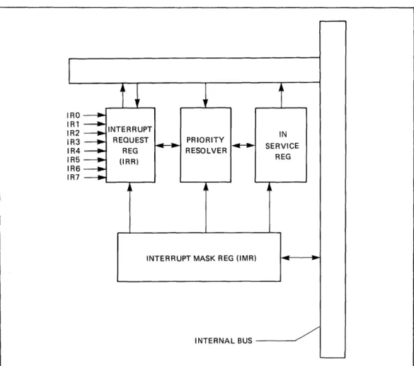
There are eight different levels of system interrupts,
Interrupt Request Register (IRR) and In-Service Register (ISR) The interrupts at the IR input lines are handled by two registers in cascade, the interrupt Request Register (IRR) and the
in-Service Register (ISR). The IRR is used to store all the interrupt levels which are requesting service, and the ISR is used to store all the interrupt levels which are being serviced.
8259A MASTER
..
INTA-
IRO80186 INT. IN INT
•
..
IR7
-80186 CAS2
~
-INT 0
-
~iNf1
-
-
SLAVE SELECT DECODER PAL INT 2-INT 3 80186 SLAVE INTERRUPT OUTPUT
Figure 5-2. Master/Slave PIC Configuration
Table 5-4 Interrupt Controller Register Offsets
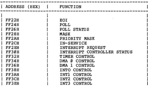
ADDRESS (HEX)
FF22H FF24H FF26H FF28H FF2AH FF2CH FF2EH FF30H FF32H FF34H FF36H FF38H FF3AH FF3CH FF3EH FUNCTION EOI POLL
POLL STATUS MASK
PRIORITY MASK IN-SERVICE
INTERRUPT REQUEST
INTERRUPT CONTROLLER STATUS TIMER CONTROL
DMA 0 CONTROL DMA I CONTROL INTO CONTROL INTI CONTROL INT2 CONTROL INT3 CONTROL
REG (lRR)
PRIORITY RESOLVER
INTERRUPT MASK REG (lMR)
IN
SERVICE REG
INTERNAL BUS
~
Prior ity Resol ver
This logic block determines the user-defined priorities of the bits set in the IRR. The highest priority is selected and
strobed into the corresponding bit of the ISR during INTA* pulse.
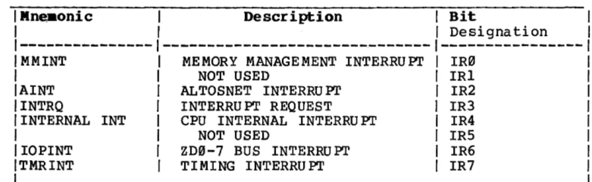
The Interrupt Mask Register (IMR) allows the user to prevent (mask) an interrupt. During a particular application, if the parity failure interrupt occurs, it can be ignored. The mask allows the user to state at a given time which of those inter-rupts, listed in Table 5-5 is going to be accepted.
Table 5-5 Systea Maskable Interrupts
IMn~aonic 1 Description 1 Bit
1 I I Designation
1---·---
1---1 MMINT 1 MEMORY MANAGEMENT INTERRUPI' I IR0
1 I NOT USED I IRl
IAINT 1 ALTOSNET INTERRUPI' I IR2 1 INTRQ I INTERRU PT REQUEST I IR3
IINTERNAL INT 1 CPU INTERNAL INTERRUPI' 1 IR4
I 1 NOT USED 1 IR5
1 IOPINT I ZD0-7 BUS INTERRUPI' I IR6
ITMRINT I TIMING INTERRU PI' I IR7
1---Master PIC Operation
When the Altos 486 Computer System is powered up, the CPU loads the initialization command word and operation command word into the PIC's internal registers, see Table 5-6. The initialization command word provides the starting address of the service
routines, while the operation command word provides the mode of operation. This mode is described below:
Fully Nested Mode - After the initialization sequence IR0 has the highest priority and IR7 the lowest.
This mode permits the PIC to operate as described above. The commands initially entered in the PIC internal registers are instructions which include what mode to enter and use. The
initial command instructions can be permanently loaded in the PIC internal registers so that it will always operate in the same mode, or the loading instructions can be modified as conditions change by reprogramming the device.
Every interrupt is assigned a type code that identifies it. A table containing up to 256 pointers defines the proper interrupt
service routine for each interrupt. Table 5-7 shows the 80186 Microprocessor predefined types and default priorities.
The Microprocessor then multiplies the 8-bit vector by four which becomes the address in a vector table. The significant five bits of the vector are user-programmable while the lower three bits are generated by the priority logic. These bits represent the encoding of the priority level requesting service. The
significant five bits of the vector are progammed by writing to the interrupt vector register at offset 20H.
Table 5-6 Master PIC Register Offsets
I Address (HEX) I Function I Type I
1---1---1---1
I 2C0 H I READ OR WRITE I CONTROL I
I 2C2H I READ OR WRITE I CONTROL I
I I I I
Table 5-7
I I
IInterrupt Name I
1---IDivide Error I Exception ISingle step I Interrupt INMI
IBreakpoint I Interrupt IINTO Detected I Overflow I Exception IArray Bounds I Exception IUnused-Opcode I Exception IESC Opcode
I Exception I ITimer 0 interrupti ITimer 1 interrupti ITimer 2 interrupti
IReserved I
IDMA 0 interrupt I IDMA 1 interrupt I IINTO interrupt I I INTI interrupt I IINT2 interrupt I IINT3 interrupt I
80186 Microprocessor Predefined Types and Default Priority
Vector I Default I Related Type I Priority I Instructions
---
---0 *1 DIV ,1DIV
1 12**2 All
2 1 All
3 *1 INT
4 *1 INTO
5 *1 BOUND
6 *1 Undefined
Opcodes
7 *1*** ESC Opcodes
8 2A****
18 2B****
19 2C****
9 3
10 4
11 5
12 6
13 7
14 8
NOTES:
*1. These are generated as the result of an instruction execution.
**2. Generated by the Single-Step flag bit TF in the status word. Once this bit is set, an internal single step
interrupt will occur after the next instruction
has been executed. The interrupt clears the TF bit and uses an internally supplied vector of 1. The IRET instruction is used to set the TF bit and transfer control to the next instruction to be single-stepped.
****3. All three timers constitute one source of request to the interrupt controller. Among the timer interrupts,
priority 2A is higher priority than 2B and 2B is higher than 2C. Each Timer interrupt has a separate
vector type number.
4. Default priorities for the interrupt sources are used only if you do not program each source into
a unique priority level.
***5. The escape opcode (part of the instruction word that designates the function performed by a given instruction) will cause a trap only if the proper bit is set in the peripheral control block relocation register.
MEMORY ADDRESSING
Memory is addressed by a two component address, consisting of a l6-bit base segment and a l6-bit offset value, derived from a combination of pointer registers, instruction pointer, and immediate values.
The l6-bit base values are contained in the one of four internal segment registers. The physical address is calculated by
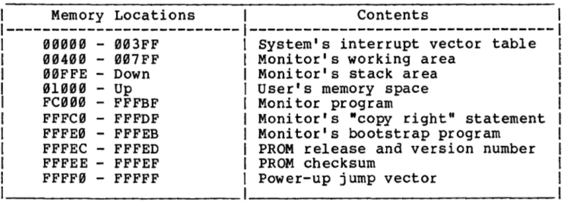
shifting the base value LEFT by four bits and adding the l6-bit offset value to yield a 20-bit physical address. This allows the 80186 to access up to 1 Mbyte of physical main memory, if it were available for the system. With expansion memory, the 486 system can hold up to 896 Kbytes of main memory. 512 Kbytes is contained in the standard configuration. Table 5-8 shows a memory map of the system.
Table 5-8 System Memory Map
Memory Locations 1 Contents
---1---
eeeee ee4ee eeFFE eleee FCeee FFFCe FFFEe FFFEC FFFEE FFFFe - rtH'3FF ee7FF Down - Up - FFFBF - FFFDF - FFFEB FFFED FFFEF - FFFFFMEMORY MANAGEMENT UNIT
System's interrupt vector table Monitor's working area
Monitor's stack area User's memory space Monitor program
Monitor's "copy right" statement Monitor's bootstrap program PROM release and version number PROM checksum
Power-up jump vector
The MMU (memory management unit) performs memory mapping and management, and provides access protection and violation detection for the mapped locations.
Memory Mapping
The MMU changes the upper eight bits of the XLA bus, generates four attribute protection bits to the BD bus, then combines these bits with the remaining lower bits from the XLA bus to produce the mapped address bus to main memory.
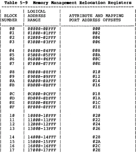
The translation of the XLA bus to the MP bus is controlled by a "mapper" in the MMU circuitry. The mapper is a collection of 256 relocation registers, see Table 5-9. Each register maps a 4K byte page of main memory. This gives a possible total of I Mbyte of memory.
Memory mapping is important in a multi-user environment because it keeps different users' programs from interfering with the operating system and with each other. Allocation of memory for each user is performed by the operating system.
Protection Function
Memory protecton allows several different programs ("tasks" or "processes") to use the same physical memory without interfering with the operating system and other user programs. Before
running a particular program, the CPU sets up the MMO to map the logical address space of the CPU into the physical memory
reserved for that program.
determined by the map. This is done through the protection attribute bits discussed later in this section.
Two type s of maps reside in the MMU, one for the oper ating system and one for user programs. In user mode, a user map is selected and the processor may not execute priviledged I/O. These are instructions whose execution could compromise the integrity of the operating system.
The set of priviledged instructions only includes I/O
instructions. The operating system always changes the CPU to be in user mode before transferring control to a user program. Therefore, if the MMU maps are accessed by I/O instructions, a user program cannot access the maps. Of course, all other I/O must also be done by the operating system, since only it can execute I/O instruction~
Table 5-9 Memory Manageaent Re1ocation Registers
I LOGICAL
I BLOCK ADDRESS ATTRIBUTE AND MAPPING NUMBER RANGE PORT ADDRESS OFFSETS
00 00000-00FFF 000
01 01000-01FFF 002
02 02000-02FFF 004
03 03000-03FFF 006
04 04000-04FFF 008
05 05000-05FFF 00A
06 06000-06FFF 00C
07 07000-07 FFF 00E
08 08000-08FFF 010
09 09000-09FFF 012
0A 0A000-0AFFF 014
0B 0B000-0BFFF 016
0C 0C000-0CFFF 018
0D 0D000-0DFFF 01A
0E 0E000-0EFFF 01C
0F 0F000-0FFFF 01E
10 10000-10FFF 020
11 11000-11FFF 022
12 12000-12FFF 024
13 13000-13FFF 026
14 14000-14FFF 028
15 15000-15FFF 02A
16 16000-16FFF 02C
17 17000-17FFF 02E
Table 5-9 (Cont'd): Memory Management Relocation Registers
LOGICAL
1
BLOCK ADDRESS 1 ATTRIBUTE AND MAPPING
NUMBER 1 RANGE 1 PORT ADDRESS OFFSETS
---1---1---18 1 18000-18FFF 1 030 19 1 19000-19FFF I 032 lA I lA000-1AFFF 1 034
IB IB000-1BFFF I 036
1
lC lC000-1CFFF I 038
ID ID000-1DFFF 1 03A
IE lE000-1EFFF I 03B
IF IF000-1FFFF I 03E
1
20 20000-20FFF 1 040
21 21000-21FFF I 042
22 22000-22FFF I 044
23 23000-23FFF 1 046
24 24000-24FFF 048
25 25000-25FFF 04A
26 26000-26FFF 04C
27 27000-27FFF 04E
28 28000-28FFF 050
29 29000-29FFF 052
2A 2A000-2AFFF 054
2B 2B000-2BFFF 056
2C 2C000-2CFFF 058
2D 2D000-2DFFF 05A
2E 2E000-2EFFF 05C
2F 2F000-2FFFF 05E
30 30000-30FFF 060
31 31000-31FFF 062
32 32000-32FFF 064
33 33000-33FFF 066
34 34000-34FFF 068
35 35000-35FFF 06A
36 36000-36FFF 06C
37 37000-37FFF 06E
38 38000-38FFF 070
39 39000-39FFF 072
3A 3A000-3AFFF 074
Table 5-9 (Cont'd): Meaory Management Relocation Registers
I LOGICAL I
BLOCK I ADDRESS / ATTRIBUTE AND MAPPING NUMBER / RANGE I PORT ADDRESS OFFSETS
---/---
---3C I 3C000-3CFFF 078
3D 3D000-3DFFF 07A
3E 3E000-3EFFF 07C
3F 3F000-3FFFF 07E
40 40000-40FFF 080
41 41000-41FFF 082
42 42000-42FFF 084
43 43000-43FFF 086
44 44000-44FFF 088
45 45000-45FFF 08A
46 46000-46FFF 08C
47 47000-47FFF 08E
48 48000-48FFF 090
49 49000-49FFF 092
4A 4A000-4AFFF 094
4B 4B000-4BFFF 096
4C 4C000-4CFFF 098
4D 4D000-4DFFF 09A
4E 4E000-4EFFF 09C
4F 4F000-4FFFF 09E
50 50000-50FFF 0A0
51 51000-51FFF 0A2
52 52000-52FFF 0A4
53 53000-53FFF 0A6
54 54000-54FFF 0A8
55 55000-55FFF 0AA
56 56000-56FFF 0AC
57 57000-57FFF 0AE
58 58000-58FFF 0B0
59 59000-59FFF 0B2
SA 5A000-5AFFF 0B4
5B 5B000-5BFFF 0B6
5C 5C000-5CFFF 0B8
5D 5D000-5DFFF 0BA
5E 5E000-5EFFF 0BC
SF 5F000-5FFFF 0BE
Table 5-9 (Cont'd): Memory Management Relocation Registers
LOGICAL
BLOCK ADDRESS ATTRIBUTE AND MAPPING NUMBER RANGE PORT ADDRESS OFFSETS ---
---
---60 60000-60FFF 0C0
61 61000-61FFF 0C2
62 62000-62FFF 0C4
63 63000-63FFF 0C6
64 64000-64FFF 0C8
65 65000-65FFF 0CA
66 66000-66FFF 0CC
67 67000-67FFF 0CE
68 68000-68FFF 0D0
69 69000-69FFF 0D2
6A 6A000-6AFFF 0D4
6B 6B000-6BFFF 0D6
6C 6C000-6CFFF 0D8
6D 6D000-6DFFF 0DA
6E 6E000-6EFFF 0DC
6F 6F000-6FFFF 0DE
70 70000-70FFF 0E0
71 71000-71FFF 0E2
72 72000-72FFF 0E4
73 73000-73FFF 0E6
74 74000-74FFF 0E8
75 75000-75FFF 0EA
76 76000-76FFF 0EC
77 77000-77FFF 0EE
78 78000-78FFF 0F0
79 79000-79FFF 0F2
7A 7A000-7AFFF 0F4
7B 7B000-7BFFF 0F6
7C 7C000-7CFFF 0F8
7D 7D000-7DFFF 0FA
7E 7E000-7EFFF 0FC
Table 5-9 Memory Management Relocation Registers
1
LOGICALI BLOCK
1
ADDRESS ATTRIBUTE AND MAPPING1
NUMBER1
RANGE PORT ADDRESS OFFSETS---1---
---80
1
80000- 80FFF 10081
1
81000-81FFF 10282
1
82000- 82FFF 10483
1
83000-83FFF 1061
84
1
84000-84FFF 10885
1
85000- 85FFF 10A86
1
86000-86FFF 10C87 87000-B7FFF 10E
8B B8000-BBFFF 110
B9 89000-B9FFF 112
BA 8A000-BAFFF 114
BB BB000-BBFFF 116
BC 8C000-BCFFF lIB
8D BD000-BDFFF llA
BE BE000-BEFFF llC
8F BF000-BFFFF lIE
90 90000-90FFF 120
91 91000-91FFF 122
92 92000-92FFF 124
93 93000-93FFF 126
94 94000-94FFF 12B
95 95000-95FFF 12A
96 96000-96FFF 12C
97 97000-97FFF 12E
9B 9B000-9BFFF 130
99 99000-99FFF 132
9A 9A000-9AFFF 134
9B 9B000-9BFFF 136
9C 9C000-9CFFF 13B
9D 9D000-9DFFF 13A
9E 9E000-9EFFF 13C
9F 9F000-9FFFF 13E
Table 5-9 (Cont'd): Memory Management Relocation Registers
---I LOGICAL
I BLOCK I ADDRESS ATTRIBUTE AND MAPPING
I NUMBER I RANGE PORT ADDRESS OFFSETS
---
---
---A0 A0000-A0FFF 140
Al AI000-AIFFF 142
A2 A2000-A2FFF 144
A3 A3000-A3FFF 146
A4 A4000-A4FFF 148
AS A5000-A5FFF 14A
A6 A6000-A6FFF 14C
A7 A7000-A7FFF 14E
A8 A8000-A8FFF 150
A9 A9000-A9FFF 152
AA AA000-AAFFF 154
AB AB000-ABFFF 156
AC AC000-ACFFF 158
AD AD000-ADFFF 15A
AE AE000-AEFFF 15C
AF AF000-AFFFF 15E
B0 B0000-B0FFF 160
Bl BI000-BIFFF 162
B2 B2000-B2FFF 164
B3 B3000-B3FFF 166
B4 B4000-B4FFF 168
B5 B5000-B5FFF 16A
B6 B6000-B6FFF 16C
B7 B7000-B7FFF 16E
B8 B8000-B8FFF 170
B9 B9000-B9FFF 172
BA BA000-BAFFF 174
BB BB000-BBFFF 176
BC BC000-BCFFF 178
BD BD000-BDFFF 17A
BE BE000-BEFFF 17C
BF BF000-BFFFF 17E
---Table 5-9 (Cont'd): Keaory Manage_ent Relocation Registers
I LOGICAL
1
BLOCK I ADDRESS ATTRIBUTE AND MAPPING
1
NUMBER RANGE I PORT ADDRESS OFFSETS I---
---1---1
C0 C0000-C0FFF I 180
1
Cl C1000-C1FFF I 182
1
C2 C2000-C2FFF I 184
1
C3 C3000-C3FFF I 186
1
I
C4 C4000-C4FFF 188 I
CS CS000-CSFFF 18A I
C6 C6000-C6FFF 18C I
C7 C7000-C7FFF 18E I
I
C8 C8000-C8FFF 190
C9 C9000-C9FFF 192
CA CA000-CAFFF 194
CB CB000-CBFFF 196
CC CC000-CCFFF 198
CD CD000-CDFFF 19A
CE CE000-CEFFF 19C
CF CF000-CFFFF 19E
D0 D0000-D0FFF 1A0
Dl D1000-D1FFF lA2
D2 D2000-D2FFF 1A4
D3 D3000-D3FFF 1A6
D4 D4000-D4FFF 1A8
DS DS000-DSFFF 1AA
D6 D6000-D6FFF lAC
D7 D7000-D7FFF 1AE
D8 D8000-D8FFF 1B0
D9 D9000-D9FFF lB2
DA DA000-DAFFF 1B4
DB DB000-DBFFF lB6
DC DC000-DCFFF lB6
DD DD000-DDFFF 1BA
DE DE000-DEFFF lBC
DF DF000-DFFFF lBE
Table 5-9 (Cont'd): Memory Mana.gement Relocation Registers
1
LOO I CAL1
1
BLOCK ADDRESS ATTRIBUTE AND MAPPING1
1
NUMBER RANGE PORT ADDRESS OFFSETS1
---
--- ---1
E0 E0000-E0FFF lC0
1
El El000-ElFFF lC2
1
E2 E2000-E2FFF lC4
1
E3 E3000-E3FFF lC6
1
E4 E4000-E4FFF lC8
E5 E5000-E5FFF lCA
E6 E6000-E6FFF ICC
E7 E7000-E7FFF ICE
E8 E8000-E8FFF lD0
E9 E9000-E9FFF lD2
EA EA000-EAFFF lD4
EB EB000-EBFFF lD6
EC EC000-ECFFF lD8
ED ED000-EDFFF IDA
EE EE000-EEFFF lDC
EF EF000-EFFFF IDE
F0 F0000-F0FFF lE0
Fl F1000-FlFFF lE2
F2 F2000-F2FFF lE4
F3 F3000-F3FFF lE6
F4 F4000-F4FFF lE8
F5 F5000-F5FFF lEA
F6 F6000-F6FFF lEC
F7 F7000-F7FFF lEE
F8 F8000-F8FFF lF0
F9 F9000-F9FFF lF2
FA FA000-FAFFF lF4
FB FB000-FBFFF lF6
FC FC000-FCFFF lF8
FD FD000-FDFFF lFA
FE FE000-FEFFF lFC
Protection Bits
Four bits from the mapper contain the protection code that are sent via the BD Bus to the MMU. These bits are called ALLOWSYWR, ALLOWUSRWR, ALLOWUSRACC and BOSPACE. The first three bits allow
system write access, user write access, or user read access to the given 4K page. The last bit is used for a stack warning indicator. If an access takes place within 128 bytes above the bottom of a page so marked then a stack warning is given to the CPU.
The "allow" bits are set by the operating system. When the system is in user mode, the user may be allowed read and write access or neither depending on the accessed page. When the system is in supervisor mode, write access may be denied on some pages.
Violation Detection
The bits in the violation port are defined in Table 5-10. All of these violations are latched and can be read via the Violation Port address offset 2F0 through 2FE. When these violations are detected, they cause an NMI to the processor.
After a violation has occurred, further violations will not pro-duce non-maskable interrupts until the current violation has been cleared. Violations can be cleared by performing an I/O instruction to the control port register 296H.
Normally, only one violation bit will be set in the violation port if an error occurs. However, if another violation occurs before the first violation has been cleared, then the new lation will be detected and latched so that more than one vio-lation bit could be set. No information is given about which violation occurred first. In addition, only the address of the first violation is latched.
I BIT
1
2 3
4
5-15
Table 5-10 Violation Port Bits
NAME
user Access Violation (read/write/op code fetch) User Write Violation System Write Violation parity Error
End of Stack Warning Not Used
SYSTEM CONTROL PORT
The system control decoder port (See Table 5-11) is a decoder PAL (Programable Array Logic) chip which performs some important tasks for the system. This port does the following:
1) Enables the output of an MMU PAL (through the "read
violation" command) so that memory cycles can take place.
2) Clocks a flip flop to enable the system to read critical control bits, (See Tables 5-11 and 5-12) at ~l~ control bits register.
3) Sets up a timer interrupt to the external PIC, See Table 5-11 for register information.
Table 5-11 Control Port Address Offsets
I
ADDRESS (HEX)1
FUNCT ION1
1---1
1
292H1
READ VIOLATION PORT1
I 296H 1 CONTROL BITS REG 1
1
298H1
CLRTlMER INT1
1---1---1
Table 5-12 Control Bits
1 BIT NO. I FUNCl' ION 1 3 Clear Parity Error*
1 4 Req ue st User Mode
I 7 Clear Violation Port*
1 14 Clear Memory Management Unit* 1
1---1
1 *Active low. 1
8255A PERIPHERAL INTERFACE ADAPTER (PIA)
The 8255A is a three-port general-purpose I/O device that performs the following functions.
1) Interfaces the floppy drive circuitry to the data and LA buses.
2) Provides a non-maskable interrupt (channel attention) signal to the Z-80A I/O processor.
3) Supplies maskable interrupts to the 80186 section from various sources.
There are three types of registers within the 8255A, data,
Table 5-13 PIA Port Address Offsets
ADDRESS (HEX) I FUNCTION
---_._---2D0 I PORT A READ OR WRITE 2D2 I PORT B READ OR WRITE 2D4 I PORT C READ OR WRITE 2D6 I CONTROL/BIT SET REGISTER
Three basic modes of operation may be selected under program control mode 0--basic I/O; mode l--strobed I/O; mode
2--bidirectional bus. Port C, under modes 1 and 2 operation, provide control (handshaking) signals for asynchronous operation. Modes 1 and 2 are also supported by interrupt I/O capability.
FLOPPY DISK CONTROLLER OPERATION
The Floppy Disk Controller (FDC) is an LSI chip, the uPD765, which contains the circuitry for interfacing a processor to the disk drive. In this application, it supports a single double-sided, double-density (MFM) 5-1/4 inch drive. The FDC has a buil t-in data separator.
The FDC shares one of the two DMA channels with the Hard Disk Controller board. Thus the processor need only load the command into the FDC, after which the data transfer occurs under control of the FDC and the 80186. The FDC is capable of multisector transfers.
Fifteen commands can be executed by the FDC, including the basic read, write, scan, format, seek, recalibrate, sense status, and their variations. Details of each command are found in the manufacturer's data handbook.
Programming
Two internal registers in the FDC may be accessed by_ the 80186 a status register and a data register See Table 5-14 and 5-15. The 8-bit status register may be read at any time. The data register actually consists of a stack of 8-bit registers, only one of which can be latched to the bus at one time.
The track stepping rate, head load time, and head unload time, are not programmable in this application but are hardwired into the controller circuitry.
Table 5-14 Floppy Disk Control Port Address Offsets
1
ADDRESS (HEX) FUNCTION---1 280H MAIN STATUS REG
1 282H COMMAND/DATA REG
Table 5-15 Floppy Disk Controller Port Address Offsets
1 ADDRESS (HEX) FUNCl'ION
---1 2E0H DACK PORT
Z-80A I/O CONTROLLER
This section describes the function of the Z-80A I/O controller and how it communicates with the 80186 processor.
Functional Description
The Z-80A microprocessor performs I/O processing for the five RS232 channels (four user ports and a serial printer port). The I/O processing circuitry includes three Z-80A SIO (serial input/ output) devices, two 8253 counters, 4K of RAM and a control ROM for the processor. The 4K of RAM is used for temporary storage and buffering. See Tables 5-16, 5-17 and 5-18.
Table 5-16 Z-SIA Port Assignaents
Z-80 ADDRESS 1 ASSIGNMENT 1
---1---1
00H - 03H 1 SI00 104H - 07H 1 SIOI 1
08H - 0BH 1 SI02 1
0CH 1 RDPERR 1
10H - 13H 1 TMRI 1
14H - 17H 1 TMR2 1
18H 1 CONTROL LATCH 1
lCH 1 ADR LATCH 1
Table

![Crystal structure of 2 [(3S,4S) 4 (anthracen 9 yl) 1 (4 methoxyphenyl) 2 oxoazetidin 3 yl] 2 aza 2H phenalene 1,3 dione unknown solvate](data:image/gif;base64,R0lGODlhAQABAIAAAP///wAAACH5BAEAAAAALAAAAAABAAEAAAICRAEAOw==)