Characterization of graphene-silicon Schottky barrier diodes using impedance
spectroscopy
Chanyoung Yim, Niall McEvoy, and Georg S. Duesberg
Citation: Applied Physics Letters 103, 193106 (2013); doi: 10.1063/1.4829140
View online: http://dx.doi.org/10.1063/1.4829140
View Table of Contents: http://scitation.aip.org/content/aip/journal/apl/103/19?ver=pdfcov
Published by the AIP Publishing
Articles you may be interested in
Schottky barrier inhomogeneity for graphene/Si-nanowire arrays/n-type Si Schottky diodes Appl. Phys. Lett. 104, 133506 (2014); 10.1063/1.4870258
Impedance characterization of AlGaN/GaN Schottky diodes with metal contacts Appl. Phys. Lett. 102, 141607 (2013); 10.1063/1.4801643
Gate tunable graphene-silicon Ohmic/Schottky contacts Appl. Phys. Lett. 101, 223113 (2012); 10.1063/1.4768921
Modified, semiconducting graphene in contact with a metal: Characterization of the Schottky diode Appl. Phys. Lett. 97, 163101 (2010); 10.1063/1.3495777
Characterization of graphene-silicon Schottky barrier diodes using
impedance spectroscopy
Chanyoung Yim,1,2Niall McEvoy,2and Georg S. Duesberg1,2,a) 1
School of Chemistry, Trinity College Dublin, Dublin 2, Dublin, Ireland
2
Centre for Research on Adaptive Nanostructures and Nanodevices (CRANN), Trinity College Dublin, Dublin 2, Dublin, Ireland
(Received 9 August 2013; accepted 17 October 2013; published online 5 November 2013)
We investigate the interface characteristics of graphene-silicon Schottky barrier diodes using dc current-voltage measurements and ac impedance spectroscopy (IS). Diode parameters, including the ideality factor and the Schottky barrier height (SBH), are extracted from the experimental data. In particular, IS makes it possible not only to define the influence of additional capacitive components due to the metal electrode contact area of the device by using a proper equivalent circuit model for the analysis but also to extract a more reliable SBH value. Therefore, we expect that IS could be widely utilized for research on the interfaces of various graphene-based devices.
VC 2013 AIP Publishing LLC. [http://dx.doi.org/10.1063/1.4829140]
Graphene is considered one of the most promising can-didates for future semiconductor industry applications because of its extraordinary properties.1–3 Thus far, it has drawn enormous attention from various research fields and intensive studies on its characteristics have been performed.4–7 Based on its unique electrical properties, a number of works on electronic device applications8–12have been carried out. Furthermore, its high conductivity makes it suitable for replacing traditional metal electrodes in diodes, which results in the formation of a Schottky contact with various semiconducting materials.13,14 In particular, the graphene-semiconductor Schottky contact structure has recently been employed in graphene-based devices such as solar cells,15–17 barristors,18 and sensors.19 Therefore, the investigation of Schottky contacts between graphene and semiconductors, which is the simplest but one of the most widely used structures in graphene-based devices, can be considered an important topic in graphene device application research. It is therefore essential to define the electrical char-acteristics of graphene-semiconductor interfaces in order to comprehensively understand the current transport mecha-nism at the interface.
In this work, we fabricated graphene-silicon (G-Si) Schottky barrier diode (SBD) devices and characterized the interface between graphene and silicon electrically using dc current-voltage (J-V) measurements and ac impedance spec-troscopy (IS) analysis. IS has primarily been used to study the charge carrier transport mechanism in organic semiconductor devices and solar cells,20,21and measured impedance spectra can be electrically interpreted with a proper equivalent circuit model. Recently, we developed an extended equivalent circuit model for the electrical characterization of Schottky contacts between various conductive carbon thin films and silicon.22 In general, diode parameters, such as the ideality factor and the Schottky barrier height (SBH), are extracted through tradi-tional current-voltage (J-V) and/or capacitance-voltage (C-V) measurement methods. It is difficult to obtain reliable
junction capacitance values from SBD devices using the tradi-tional C-Vmethod, particularly when the devices have a se-ries resistance. It has been shown that the existence of sese-ries resistance in a diode device can cause considerable errors in calculation of the diode parameters,23,24but, in practice, it is not possible to make a SBD device without any series resist-ance. Here, we used IS to obtain capacitance values at the junction as this gives more reliable values than the traditional
C-Vmethod, particularly for microscopic systems with vary-ing series resistances. IS has recently been applied to the anal-ysis of the metal-semiconducting nanowire contact and the interface of carbon-silicon SBD devices with series resist-ance.22,25In this study, IS was employed for the investigation of the interface of G-Si SBD devices for an accurate analysis of the Schottky junction and to extract information about the interface between silicon and graphene.
A thermally grown silicon dioxide (SiO2) layer (150 nm)
on an n-type silicon (n-Si) wafer with a dopant (phosphorus) concentration of 51014cm3 and h100i orientation was used as a substrate for the device. A part of the SiO2 layer
was completely removed by a wet etching process with 3% diluted hydrofluoric acid (HF) for 10 min, followed by rinsing with deionized water and drying. Using a shadow mask, tita-nium (Ti) and gold (Au) metal electrodes (Ti/Au¼20/80 nm) were sputtered on the top center of the remaining SiO2layer
and the exposed n-Si area, respectively, and a good ohmic contact was achieved between Ti and n-Si. Graphene was produced using chemical vapor deposition (CVD) on copper (Cu) foils as described in detail in our previous work.26The graphene was then transferred onto the pre-patterned sub-strate, directly after removing the native oxide layer from the exposed silicon surface with HF, in order to form a direct contact between the graphene and the silicon. One end of the graphene lies on the n-Si surface without touching the metal electrode deposited on the n-Si, and the other end sits on the gold pad on the SiO2layer which insulates a direct contact
between the metal electrode and the Si substrate.
Raman spectra were obtained with a Witec Alpha 300 R microscope, using an excitation wavelength of 532 nm. J-V a)
Electronic mail: duesberg@tcd.ie
measurements were carried out on a Suss probe station con-nected with a Keithley 2612A source meter. The metal elec-trode on the SiO2 layer was positively biased, and the
electrode on the n-Si substrate was negatively biased. IS data were recorded by a Gamry Reference 600 potentiostat, and GamryEchem Analyst software was used for the data analy-sis. All the electrical measurements were performed under ambient conditions.
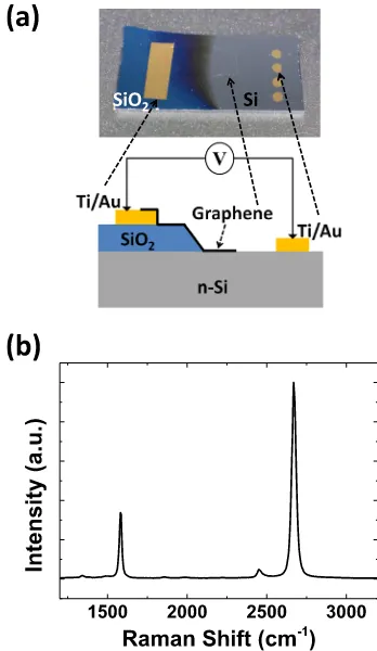
A photograph of the fabricated G-Si SBD device and its schematic diagram are depicted in Fig.1(a). The device has an effective interface area of0.2 cm2as measured by opti-cal microscopy. Fig.1(b) shows a Raman spectrum of the graphene on the SiO2part of the device which was obtained
by averaging over 6400 scans taken over a 2020lm area. It has a large 2D (at 2670 cm1) to G (at 1580 cm1) peak in-tensity ratio (I2D/IG) which is approximately 3, clearly
indi-cating that the graphene has a monolayer thickness. There is a negligible D-peak contribution underlining the high quality of the graphene. More details on the Raman data are given in the supplementary material.34
The dark current-voltage measurement data of the gra-phene/n-Si (G/n-Si) SBD device are plotted in Fig. 2(a), which shows typical rectifying behavior. The relationship between the current density (J) of the diode and the voltage drop across the junction (VD) of the Schottky junction can be
described using thermionic emission theory and it is given by the following equation:27
J¼Js exp
qVD
nkBT 1
; (1)
whereJS is the reverse saturation current density, n is the
ideality factor,kBis the Boltzmann constant,qis the
elemen-tary charge, andTis the absolute temperature in Kelvin. The reverse saturation current density (JS) can be expressed as
Js¼AT2exp q/B
kBT
; (2)
where A** is the effective Richardson constant for n-Si and
uBis the effective barrier height at zero bias. When
consider-ing the effect of the series resistance (RS) of the system, which
can stem from the resistance of the graphene and Si substrate, the contact resistances to the metal electrodes and interface states at the junction,VDof the Eq.(1)can be replaced with
the combination of the total voltage drop, V, of the system and the voltage drop due toRS. Thus,VD¼VJRS, and for
VD>3kBT/q, Eq.(1)becomes
J¼Jsexp
qðVJRsÞ
nkBT
: (3)
Cheung and Cheung outlined the extraction of diode parame-ters, like the ideality factor and the barrier height, using the
J-Vmeasurement data from a SBD device with series resist-ance.28Applying this method to our measurement data gives the values of n¼1.38 and quB¼0.69 eV. In general, the
ideality factor higher than the unity observed in real SBDs can be attributed to several factors such as the image force lowering effect, additional thermally assisted carrier tunneling
at the junction, bias dependent SBHs, and Schottky barrier inhomogeneity in the junction area.29,30 In the case of G-Si SBDs, it is known that charge puddles can be formed uninten-tionally during the graphene synthesis or transfer process, which causes Schottky barrier inhomogeneity at the interface. These factors can be quantified by calculating the flat band barrier height (uBF), where the influence of such factors on
the evaluation ofJ-Vdata does not exist, so it can be used as a fundamental value for the comparison between experimental and theoretical data.31,32uBFcan be calculated by using
/BF¼n/B ðn1Þ
kBT
q
ln Nc
Nd
; (4)
whereNcis the effective density of states in the conduction
band and Ndis the carrier density. Using this equation, the
calculated value of quBF is found to be 0.84 eV, which is
larger thanquBfrom theJ-Vmeasurement data.
Impedance spectra of the G/n-Si SBD device were obtained in the frequency range of 0.1 Hz to 1 MHz with an ac voltage of 10 mV under various dc biases (from 0.6 to
þ0.6 volts with a step of 0.1 V) at room temperature. Figs.
2(b)and2(c)show Cole-Cole impedance plots of the G/n-Si SBD under forward, zero, and reverse dc bias. The radius of the semicircles, which is related to the total impedance of the device, increases as the dc bias decreases in the forward bias region while it shows a clear upsurge in diameter in the zero and reverse bias regions. This means the impedance value of the device is dependent on the applied dc bias and it has a much larger value under reverse bias than forward bias. The
FIG. 1. (a) A photograph of the G/n-Si SBD device (top) and its schematic diagram (bottom). (b) Average Raman spectrum of high quality graphene on the SiO2layer of the device.
[image:3.612.349.523.53.353.2]nearly semi-circular shape of the impedance spectra over the whole dc bias range indicates that the Schottky junction can be expressed using an equivalent circuit model which is composed of a combination of resistance and capacitance (RC) networks.33 A typical equivalent circuit model of a Schottky junction consists of a parallel connected RC net-work and a series resistance which is serially connected to the RC network. The RC network represents the space charge region and the series resistance accounts for the con-tact and bulk resistance of the device, respectively, showing a perfect semi-circular Cole-Cole impedance plot. However, the plots of Figs. 2(b) and 2(c) do not have perfect semi-circular shapes. This implies that there is more than one RC component in the system where the contact area of each metal electrode can cause extra capacitive components in the
device. Therefore, a more complex equivalent circuit model was used for the analysis of the impedance spectra,22where the influence of the contacts between the Au pad and the gra-phene sheet and the Ti/Au electrode and the n-Si substrate are taken into account. The equivalent circuit model is pre-sented in Fig.3(a). It has three RC pairs in series connected with a series resistance (RS) and a parasitic inductance (L).
C1, C2, and C3 are the capacitances related to the
Au-graphene, graphene-Si, and Si-Ti interfaces, respectively, with corresponding shunt resistancesR1,R2, andR3. In
gen-eral, the ac impedance (Z) is expressed by
ZðxÞ ¼Z0ðxÞ jZ00ðxÞ; (5)
where xis the frequency, Z0 andZ00 are the magnitudes of the real and imaginary parts of the impedance, respec-tively.33For mathematical analysis of the equivalent circuit model in Fig.3(a),Z0andZ00can be expressed as
Z0ðxÞ ¼ R1
1þ ðxR1C1Þ 2þ
R2
1þ ðxR2C2Þ 2
þ R3
1þ ðxR3C3Þ
2þRs; (6)
Z00ðxÞ ¼ xR
2 1C1
1þ ðxR1C1Þ 2þ
xR2 2C2
1þ ðxR2C2Þ 2
þ xR
2 3C3
1þ ðxR3C3Þ
2xL: (7)
The fitted curves, with experimental data obtained under var-ious dc biases using these equations, are depicted in Figs.
3(b)–3(e), showing a good fit with each other. The resistance and capacitance values extracted from the best fit of the ex-perimental impedance data are plotted in Figs.4(a)and4(b)
with a semi-logarithmic scale for the G/n-Si SBD device. While the series resistance, RS, is constant over the whole
bias region with an average value of 13060.7X,R2shows
a significant change as the dc bias varies from the forward to reverse region. It has very high values compared to the other resistances in the reverse dc bias region, and it can be con-ceived that the R2C2 component of the equivalent circuit
model is related to the Schottky barrier at the G/n-Si inter-face because R2suppresses the current flow at the junction
under reverse dc bias. When a forward dc bias is applied, it suddenly drops dramatically with increasing bias voltage. This can be explained by considering that more current can flow through the Schottky junction since the barrier is low-ered by the forward bias, leading to a drop in the junction re-sistance. The other RC network components (R1C1 and
R3C3) of the model, related to the Au-graphene contact
(R1C1) and the Ti-Si contact (R3C3), respectively, show
rela-tively small variation over the whole dc bias region with an averaged contact resistance value of 404677Xfor R1and
88620XforR3. In the ideal case, the interfaces at the
Au-graphene and Si-Ti contacts should not be influenced by the external bias, however, imperfect surface conditions, like possible defects at the interfaces, can give rise to such varia-tion in a practical case. Even though the detailed mechanism which causes the bias dependent behavior at the metal
[image:4.612.357.560.280.399.2]electrode contact area of the device is not clearly verified, IS makes it possible to separate the effect of each electrode con-tact from the whole capacitive component of the device and quantify it using the proper equivalent circuit model.
Using the depletion capacitance (C2) of the Schottky
junction, a Mott-Schottky plot (1/C2 vs. V) can be estab-lished and information on the built-in potential (Vbi) and the
SBH (quB) of the device at the junction can be derived. 27
The Mott-Schottky plot of the G/n-Si SBD is shown in Fig.
4(c). The Vbi can be determined by linear extrapolation of
the intercept with the x axis (dc bias), giving values of
Vbi¼0.54 V and a calculated value of quB¼0.82 eV. The
value of SBH obtained from the Mott-Schottky plot is not fully consistent with the value from the previous J-V data (quB¼0.69 eV), showing an increase of 0.13 eV. This
dis-crepancy may stem from the possible presence of a thin insu-lating layer at the G-Si interface and/or Schottky barrier inhomogeneity.17,24,30 The value of SBH from the Mott-Schottky plot is in excellent agreement with the above calcu-lated flat band barrier height (quBF¼0.84 eV), underlining
the fact that IS results in a more accurate parameter extrac-tion on the SBH of the device than the dcJ-Vmeasurement method. However, it should be noted that while a dc J-V
measurement method is mainly utilized to define the current transport mechanism at the junction and the ideality factor representing the performance of diodes, an ac IS measure-ment method has merit for the characterization of the space
charge region at the junction and it can localize the effect of metal electrode contacts from the system; therefore, they are complementary for the study of the interface of SBDs.
In summary, G/n-Si SBDs were fabricated and investi-gated using dcJ-Vand ac IS measurements. An ideality factor of 1.38 and a SBH of 0.82 eV were extracted from the experi-mental data. In our work, we utilized the IS method to obtain
FIG. 3. (a) Equivalent circuit model of the G/n-Si SBD for the IS analysis whereR1C1,R2C2, andR3C3represent the RC networks related to the
inter-faces of Au-graphene, graphene-Si, and Si-Ti, respectively.RSis the series
resistance andLrepresents a parasitic inductance associated with the electri-cal leads. Cole-Cole plots and corresponding fit from the equivalent circuit model on the G/n-Si SBD under dc bias of (a)þ0.4 V, (b) 0.0 V, (c)
[image:5.612.326.549.49.608.2]0.3 V, and (d)0.5 V.
FIG. 4. Semi-logarithmic plots of (a) resistance and (b) capacitance values for dc bias voltages in the range ofþ0.6 V to0.6 V achieved from the best fit of the IS of the G/n-Si SBD using the equivalent circuit model of Fig. 3(a). (c) The Mott-Schottky plot (1/C2vs.V) of the G/n-Si SBD withC2
val-ues extracted from the simulated results using the equivalent circuit model of Fig.3(a).
[image:5.612.56.293.391.692.2]a more reliable SBH value using a proper equivalent circuit model for the analysis. It is expected that this kind of approach to the investigation of graphene-based nanoscale devices will allow the interface of the devices to be inter-preted in a more comprehensive and detailed way. This is of particular importance because most graphene SBDs are not completely free from the effect of metal electrode contacts and also the graphene-semiconductor interfaces may not be ideal. Thus, this study will facilitate graphene-based device developments, particularly for diodes, sensors, and solar cells.
This work was supported by the SFI under Contract Nos. 08/CE/I1432 and PI_10/IN.1/I3030 (PICA). C.Y. acknowledges the Embark Initiative via an Irish Research Council scholarship.
1
K. S. Novoselov, A. K. Geim, S. V. Morozov, D. Jiang, Y. Zhang, S. V. Dubonos, I. V. Grigorieva, and A. A. Firsov,Science306, 666 (2004).
2A. K. Geim and K. S. Novoselov,Nature Mater.6, 183 (2007).
3A. H. Castro Neto, F. Guinea, N. M. R. Peres, K. S. Novoselov, and A. K.
Geim,Rev. Mod. Phys.81, 109 (2009).
4
M. Ishigami, J. H. Chen, W. G. Cullen, M. S. Fuhrer, and E. D. Williams, Nano Lett.7, 1643 (2007).
5B. Das, R. Voggu, C. S. Rout, and C. N. R. Rao,Chem. Commun.
2008, 5155.
6
M. Terrones, A. R. Botello-Mendez, J. Campos-Delgado, F. Lopez-Urias, Y. I. Vega-Cantu, F. J. Rodriguez-Macias, A. L. Elias, E. Munoz-Sandoval, A. G. Cano-Marquez, J.-C. Charlier, and H. Terrones, Nanotoday5, 351 (2010).
7
J. Krupka and W. Strupinski,Appl. Phys. Lett.96, 082101 (2010).
8F. Xia, D. B. Farmer, Y.-m. Lin, and P. Avouris, Nano Lett. 10, 715
(2010).
9
T. Feng, D. Xie, Y. Lin, Y. Zang, T. Ren, R. Song, H. Zhao, H. Tian, X. Li, H. Zhu, and L. Liu,Appl. Phys. Lett.99, 233505 (2011).
10F. Chen, Q. Qing, J. Xia, J. Li, and N. Tao,J. Am. Chem. Soc.131, 9908
(2009).
11
G. P. Keeley, A. O’Neill, N. McEvoy, N. Peltekis, J. N. Coleman, and G. S. Duesberg,J. Mater. Chem.20, 7864 (2010).
12G. P. Keeley, A. O’Neill, M. Holzinger, S. Cosnier, J. N. Coleman, and G.
S. Duesberg,Phys. Chem. Chem. Phys.13, 7747 (2011).
13
S. Tongay, M. Lemaitre, T. Schumann, K. Berke, B. R. Appleton, B. Gila, and A. F. Hebard,Appl. Phys. Lett.99, 102102 (2011).
14C.-C. Chen, M. Aykol, C.-C. Chang, A. F. J. Levi, and S. B. Cronin,Nano
Lett.11, 1863 (2011).
15
X. Li, H. Zhu, K. Wang, A. Cao, J. Wei, C. Li, Y. Jia, Z. Li, X. Li, and D. Wu,Adv. Mater.22, 2743 (2010).
16
L. Lancellotti, T. Polichetti, F. Ricciardella, O. Tari, S. Gnanapragasam, S. Daliento, and G. Di Francia,Thin Solid Films522, 390 (2012).
17
X. Miao, S. Tongay, M. K. Petterson, K. Berke, A. G. Rinzler, B. R. Appleton, and A. F. Hebard,Nano Lett.12, 2745 (2012).
18H. Yang, J. Heo, S. Park, H. J. Song, D. H. Seo, K.-E. Byun, P. Kim, I.
Yoo, H.-J. Chung, and K. Kim,Science336, 1140 (2012).
19
H.-Y. Kim, K. Lee, N. McEvoy, C. Yim, and G. S. Duesberg,Nano Lett. 13, 2182 (2013).
20C. Jonda and A. B. R. Mayer,Chem. Mater.
11, 2429 (1999).
21
W. Huang, J. Peng, L. Wang, J. Wang, and Y. Cao,Appl. Phys. Lett.92, 013308 (2008).
22C. Yim, N. McEvoy, H.-Y. Kim, E. Rezvani, and G. S. Duesberg,ACS
Appl. Mater. Interfaces5, 6951 (2013).
23
A. S. Kavasoglu, N. Kavasoglu, and S. Oktik, Solid-State Electron.52, 990 (2008).
24S. Tongay, M. Lemaitre, X. Miao, B. Gila, B. R. Appleton, and A. F.
Hebard,Phys. Rev. X2, 011002 (2012).
25
J. Huh, J. Na, J. S. Ha, S. Kim, and G. T. Kim, ACS Appl. Mater. Interfaces3, 3097 (2011).
26S. Kumar, N. McEvoy, H.-Y. Kim, K. Lee, N. Peltekis, E. Rezvani, H.
Nolan, A. Weidlich, R. Daly, and G. S. Duesberg,Phys. Status Solidi B 248, 2604 (2011).
27
S. M. Sze and K. K. Ng,Physics of Semiconductor Devices, 3rd ed. (John Wiley & Sons, Inc., Hoboken, New Jersey, 2007), p. 134.
28S. K. Cheung and N. W. Cheung,Appl. Phys. Lett.
49, 85 (1986).
29
R. T. Tung,Mater. Sci. Eng. R35, 1 (2001).
30
J. H. Werner and H. H. Guttler,J. Appl. Phys.69, 1522 (1991).
31J. H. Werner and H. H. Guttler,J. Appl. Phys.73, 1315 (1993). 32
S. Tongay, T. Schumann, and A. F. Hebard,Appl. Phys. Lett.95, 222103 (2009).
33
J. R. Macdonald and W. B. Johnson, inImpedance Spectroscopy: Theory, Experiment, and Applications, edited by E. Barsoukov and J. R. Macdonald (John Wiley & Sons, Inc., Hoboken, New Jersey, 2005), p. 1.
34