Circuits and Systems, 2010, 1, 59-64
doi:10.4236/cs.2010.12010 Published Online October 2010 (http://www.SciRP.org/journal/cs)
Pulse Skipping Modulated Buck Converter - Modeling and
Simulation
Ramamurthy Srinivasan, Vanaja Ranjan P.
Department of EEE, College of Engineering, Guindy, Anna University, Chennai, India E-mail: [email protected]
Received August 23,2010; revised September 19,2010; accepted September 25,2010
Abstract
Modeling and simulation results of a pulse skipping modulated buck converter for applications involving a source with widely varying voltage conditions with loads requiring constant voltage from full load down to no load is presented. The pulses applied to the switch are blocked or released on output voltage crossing a predetermined value. The regulator worked satisfactorily over a wide input voltage range with good transient response but with higher ripple content. Input current spectrum indicates a good EMI performance with crowding of components at audio frequency range for the selected switching frequency.
Keywords:DC/DC Converter, Pulse Skipping Modulation, Buck Regulator, Modulation Factor,
Electromagnetic Interference
1. Introduction
DC-to-DC buck converters are direct converters em-ployed for stepping down DC voltage to a desired lower level. These are employed, due to their inherent high efficiency, in places where losses due to their linear counterparts are not tolerated. A buck regulator is a suitably controlled buck converter that can maintain its output voltage at the desired level during constant load with varying input voltage conditions, constant input voltage with varying load conditions or both. A voltage mode PWM controller, in which the duty cycle is altered, based on error between set voltage and measured output voltage such that the output voltage of the converter is very nearly equal to the desired value is well documented and widely used [1-4]. These converters are mostly based on circuits in which a pulse width modulated (PWM) signal is filtered with an LC network [5-7]. Apart from maintaining the line and load regulations low, it is also desirable to retain the losses low especially in applica-tions involving energy limited sources. It is required that the efficiency is kept high throughout the operating range. Efficiency of PWM switching regulators is in general high compared to linear regulators but not constant over the entire load range. Efficiency of a PWM regulator at light loads is significantly less compared to that at near full load conditions. The problem is pronounced at low voltage portable applications. Various topologies and
methods of control were suggested and synchronous buck topology with ZVS technique is suggested for minimizing switching losses [8-10]. The low side MOS-FET device with integrated Schottky diode can further improve the efficiency of synchronous converter even though there is slight increase in ON resistance [11].
The converter, which operates with high efficiency at light loads during stand by mode, in which portable equipment operate most of the time when not in use, de-manded considerable attention of the researchers and several techniques including improved controllers with digital PWM, PFM with reduced switching and conduc-tion losses were proposed [12-14]. Pulse Skipping Mo- dulated Converters operate with higher efficiency at light loads with reduced switching loss due to pulse skipping [15]. A pulse skipping modulated DC-DC converter is studied in this paper for its performance under varied supply and load conditions.
2. Pulse Skipping Modulated Buck
Converter
2.1. Description
A pulse skipping modulated buck converter is shown in
RAMAMURTHY S. ET AL. 60
40kHz V1
0/1V +
-Vref L
C +
-Vin R
40kHz V1
0/1V +
-Vref L
C +
-Vin R
[image:2.595.65.280.75.235.2]PSM Control
Figure 1. Pulse skipping modulated buck converter.
frequency is well below the switching frequency. The feedback circuit consists of a PSM control logic, which allows the pulse generated by the clock if actual voltage is below the reference voltage and skips pulses if the actual voltage exceeds the reference voltage vref. The
clock pulse generated is a constant frequency constant width (CFCW) pulse [16]. MOSFET switch is ON when the clock pulse is applied over a fixed duration of time equal to duty cycle of the clock and the inductor current rises linearly. The switch is OFF for the remaining pe-riod of the cycle and the current drops to a lower value but higher than the initial value of the cycle. It drops to a value lower than the initial value if the next pulse is skipped and so on. Thus by alternately permitting p pulses and skipping q pulses the output voltage is main-tained at a value close to reference value. The waveforms are shown in Figure 2.
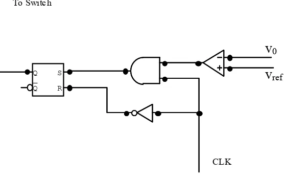
[image:2.595.103.499.346.479.2]As shown in Figure 3, a comparator compares v0 and vref and its output is ANDed with CLK. Output of AND gate sets RS flip flop which is reset at the falling edge of the clock as shown through a NOT gate. Pulse Output of the flip-flop is used to drive the converter switch. On vref > v0 comparator output is HIGH and AND gate output sets flip flop every time CLK goes HIGH and is reset at the falling edge. Hence clock pulses are applied
Figure 2. Waveforms of output voltage, Inductor current and gate pulses for a PSM converter.
S R Q _
Q S
R Q _ Q
To Switch
CLK
v
0v
refFigure 3. PSM control logic.
[image:2.595.151.430.522.695.2]RAMAMURTHY S. ET AL.
to the switch. This is known as charging period. On vrefd < v0 comparator output is LOW and AND gate out put is LOW irrespective of the clock and hence the flip flop is not set and clock pulses are not applied to the switch or pulses are skipped. This is known as skipping period.
3. Modeling of PSM converter
Let for p cycles the clock pulses are applied and for q cycles the pulses are skipped for a particular load resis-tance R and input voltage Vin. The duration pT is known as charging period and the duration qT is known as skip ping period. During the charging period, in each cycle the switch is ON for duration equal to D and during the skipping period the switch is OFF throughout as the pulses are not applied and skipped.
The converter is modeled [16] using state space aver-aging method and the state space equations, assuming continuous conduction mode, are obtained as shown be-low.
During charging period,
1 1
1
0
in
x A x B v t DT
y C x
(1) 2 2 2 in
x A x B v DT t T
y C x
(2)
During skipping period,
2 2
2
0
in
x A x B v t T
y C x
(3) where, 1 2 1 0 1 1 L
A A A
C RC , L C i x v
,y v 0,
1 1 0 B L
, B20 C
0 1
After State Space Averaging,
in
p
x Ax BDv
p q
(4)
Defining Modulation Factor M,
q M
p q
Then Equation (4) becomes
1
inxAx M DBv (5) Hence the average output voltage is given by
0 1 in
V M Dv (6)
M, the modulation factor is a measure of the number of skipping. When vin goes higher for the same V0with
constant D, M increases increasing the number of skipped pulses to maintain the voltage. Similarly when load decreases M increases decreasing the number of switching. When no pulses are skipped then M is zero and the equation reduces to that of a buck converter without feedback at steady state.
4. Simulation
Simulation of the PSM DC-DC buck converter was car-ried out with the following parameters. vin = 12 V to 20
V, V0 = 5 V, L = 150 H, C = 20 F, f = 40 KHz.
Pulses are skipped to regulate the output voltage with increase in input voltage as shown in Figure 4.
Input voltage is stepped from 12 V to 20 V and the output voltage is plotted. Output voltage waveform for a constant load with a step increase in input voltage is shown in Figure 5.
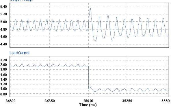
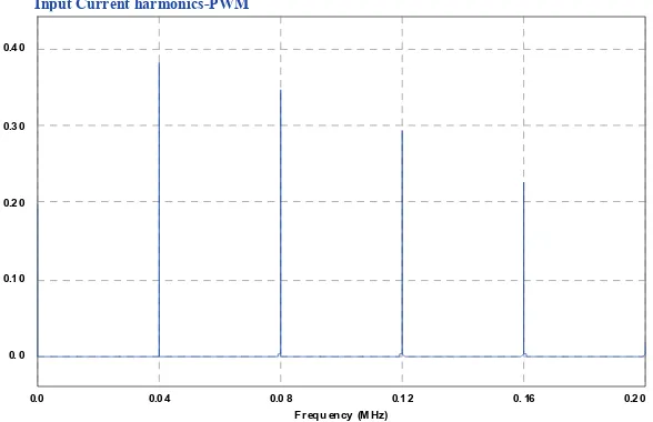
Response showed that PSM converter can accept wide variations in input voltage and its response speed was good as seen from step response and the output voltage was regulated over the entire range. Modulation Factor increases with increase in voltage increasing the pulses skipped Load was decreased by a step and the output voltage is shown in Figure 6. Pulses skipped increased, as load was decreased to regulate the voltage. The ripple of the output voltage was higher as input voltage was increased. A similar response was observed when the load was decreased. Input current harmonic spectrum of the PSM converter is shown in Figure 7. Spectrum of the converter with PWM control is also shown in Figure 8
for comparison purpose for the same input voltage and load.
In the case of PSM converter harmonic components are spread over a wide band of frequencies lowering the average value of the peaks of currents. Individual peaks are smaller than those of PWM converter. Hence PSM converter has better EMI performance. Due to reduction in average frequency with pulse skipping at light loads there may be components entering into audio frequency range which may result in audible noise interference, which can be avoided by selecting the switching fre-quency high.
5. Conclusions
RAMAMURTHY S. ET AL. 62
0.0 2.00 4.00 6.00 8.00
1 0.00 Puls es App lied to Swit ch
498 .50 499.0 0 499.5 0 5 00.0 0 5 00.50 5 01.00 5 01.50 50 2.00 T ime (ms )
1 0.00 1 2.00 1 4.00 1 6.00 1 8.00 2 0.00
[image:4.595.156.445.79.257.2]Sup ply Vo ltag e
Figure 4. Increased pulse skipping with input voltage increase.
495 .00 50 0.00 505.0 0 510 .00
Time (ms ) 2.00
4.00 6.00 8.00 1 0.00
[image:4.595.151.445.290.481.2]V0 fo r Vin = 12V an d 2 0V. Vref = 5V
Figure 5. Output voltage for step increase in input voltage.
4.40 4.60 4.80 5.00 5.20 5.40
Output V ol tage
345.00 347.50 350. 00 352.50 355.00
Ti me (ms) 0.80
1.00 1.20 1.40 1.60 1.80 2.00 2.20
Load Current
Figure 6. Output voltage for step decrease in load current.
Output Voltage
[image:4.595.150.446.518.703.2]RAMAMURTHY S. ET AL. 63
0.0 0.04 0.08 0.12 0.16 0.20
Frequency (MHz) 0.0
0.10 0.20 0.30 0.40
[image:5.595.145.444.85.270.2]Input Current Harmonics
Figure 7. Input current harmonic spectrum – PSM converter.
0.0 0.0 4 0.0 8 0.1 2 0. 16 0.2 0
F req u en cy (M Hz) 0. 0
0.1 0 0.2 0 0.3 0 0.4 0
In p ut Cu rre nt Harmo ni cs - PWM
Figure 8. Input current harmonic spectrum – PWM converter.
range of input voltage intended for operation. Input cur-rent harmonic spectrum was studied and compared with that of PWM controlled Converter. PSM converter has a well spread out spectrum, with individual component peak values less in amplitude, making its EMI perform-ance better than that of PWM controlled converter. But there are frequency components entering into audio fre-quency range due to the average frefre-quency of switching being lower with pulse skipping, if the switching fre-quency is selected to be just above the audio range.
6. References
[1] R. W. Erickson and D. Maksimovic, “Fundamentals of Power Electronics,” 2nd Edition, Kluwer Academic Pub- lishers,Dordrecht.
[2] A. J. Forsyth and S. V. Mollow, “Modelling and Control of DC-DC Converters,” IEE Power Engineering Journal, Vol. 12, No. 5, October 1998, pp. 229-236.
[3] J. G. Kassakian, M. F. Schlecht and G. C. Verghese, “Principles of Power Electronics,” Addison-Wesley, Reading, June 1992.
[4] B. Arbetter, R. Erickson and D. Maksimovic, “DC-DC Converter Design for Battery-Operated Systems,” IEEE PESC’95. Vol. 1, June 1995, pp. 103-109.
[5] A. J. Stratakos, S. R. Sanders and R. W. Broderson, “A Low-Voltage CMOS DC–DC Converter for a Portable Battery-Operated System,” Proceedings of Power Elec- tronics Specialists Conference, Taiwan, Vol. 1, June 1994, pp. 619-626.
[6] G. Y. Wei and M. Horowitz, “A Fully Digital, Energy- Efficient Adaptive Power-Supply Regulator,” IEEE Journal of Solid-State Circuits, Vol. 35, April 2000, pp.
[image:5.595.145.439.306.496.2]RAMAMURTHY S. ET AL. 64
520-528.
[7] A. P. Dancy, R. Amirtharajah and A. P. Chandrakasan, “High-Efficiency Multiple-Output DC–DC Conversion for Low-Voltage Systems,” IEEE Transactions on VLSI, Vol. 8, June 2000, pp. 252-263.
[8] A. V. Peterchev and S. R. Sanders, “Digital Loss – Minimizing Multi-Mode Synchronous Buck Converter Control,” 35th Annual IEEE Power Electronics Specia- lists Conference, Vol. 6, Aachen, 2004, pp. 3694-3699. [9] S. Pattnaik, A. K. Panda, K. Aroul and K. K. Mahapatra,
“A Novel Zero Voltage Transition Synchronous Buck Converter for Portable Application,” International Jour- nal of Electrical, Computer, and Systems Engineering, Vol. 2, No. 2, 2008, pp. 115-120.
[10] A. Consoli, F. Gennaro, C. Cavallaro and A. Testa, “A Comparative Study of Different Buck Topologies for High-Efficiency Low-Voltage Applications,” Proceed- ings on Power Power Electronics Specialist Conference, 1999, pp. 60-65.
[11] D. Calafut, “Trench Power MOSFET Lowside Switch with Optimized Integrated Schottky Diode,” Proceedings of the 16th International Symposium on Power Semicon- ductor Devices and ICs (ISPSD’04), 24-27 May 2004, pp. 397-400.
[12] K. M. Smith and K. M. Smedly, “A Comparison of Voltage-Mode Soft Switching Methods for PWM Converters,” IEEE Transactions on Power Electronics, Vol. 12, No. 2, 1997, pp. 376-386.
[13] X. W. Zhou, M. Donati, L. Amoroso and F. C. Lee, “Improved Light-Load Efficiency for Synchronous Rec- tifier Voltage Regulator Module,” IEEE Transactions on Power Electronics, Vol. 15, No. 5, September 2000, pp. 826-834.
[14] C.-L. Chen, W.-L. Hsieh, W.-J. L. K.-H. Chen and C.-S. Wang, “A New PWM/PFM Control Technique for Improving Efficiency over Wide Load Range,” 15th IEEE International Conference on Electronics, Circuits and Systems, Malta, 2008, pp. 962-965.
[15] P. Luo, L. Y. Luo, Z. J. Li, et al., “Skip Cycle Modulation in Switching DC-DC Converter,” Interna- tional Conference on Communications, Circuits, and Systems, Chengdu, June 2002, pp. 1716-1719.
[16] P. Luo, B. Zhang, S.-P. Wang and F. Yong, “Modeling and Analysis of Pulse Skip Modulation,” Journal of Electronic Science and Technology of China (Chinese), Vol. 4, No. 1, March 2006.
[17] A. Farhadi and A. Jalilian, “Modeling, Simulation and Reduction Techniques of Electromagnetic Conducted Emission Due to Operation of Power Electronic Conver- ters,” International Conference on Renewable Energy and Power Quality (ICREPQ’07), Sevilla, March 2007. [18] F. Lin and D. Y. Chen, “Reduction of Power Supply EMI