IEEE
Proof
design and reliability of the assembly, with a fully bondwireless8
approach using cylindrical copper bumps. Advanced numerical
9
structural simulation techniques are also applied to assess the
10
influence of interconnect characteristics (material, size, and shape)
11
and try to determine an optimum solution for reducing the stress
12
and creep strain development in the solder joint. Preliminary
13
experimental tests of the power module are also carried out at
14
different switching frequency and loads to prove the validity of
15
the proposed solution in terms of electromagnetic performance.
16
Index Terms—Copper bump, flip-chip, power electronics
pack-17
aging, solder joint, thermomechanical stress.
18
I. INTRODUCTION 19
T
HIS paper addresses the reliable integration of a half-20bridge switch (HBS) based on last generation 70-μm-21
thin 600-V/200-A insulated-gate bipolar transistors (IGBTs) 22
and diodes; in particular, it advances the state of the art as 23
regards a recently presented packaging concept, which targets 24
the optimization from an application point of view [1]. In 25
the application, two transistors with antiparallel diodes need 26
to be connected in series (high-side and low-side switch) to 27
build a half-bridge power switch (HBS) configuration, as ex-28
tensively required, for instance, by synchronous rectified dc–dc 29
converters and by dc–ac converters (i.e., inverters). During 30
operation within such power converter topologies, load current 31
commutations always take place between high-side transistor 32
and low-side diode (Cell-P) and, vice versa, between low-side 33
transistor and high-side diode (Cell-N). Current commutation 34
between antiparallel transistor–diode pairs only takes place 35
at zero voltage in the case of synchronous rectified dc–dc 36
converters, and at zero current in the case of inverters, and 37
is thus, by definition, noncritical in both cases (i.e., it does 38
not imply power dissipation or potentially destructive voltage 39
Manuscript received October 29, 2013; revised April 5, 2014; accepted May 21, 2014. Paper 2013-PEDCC-710.R1, presented at the 2012 IEEE Energy Conversion Congress and Exposition, Raleigh, NC, USA, September 15–20, and approved for publication in the IEEE TRANSACTIONS ON INDUSTRY
APPLICATIONSby the Power Electronic Devices and Components Committee of the IEEE Industry Applications Society.
The authors are with the Power Electronics Machines and Control Group, The University of Nottingham, Nottingham, NG7 2RD, U.K. (e-mail: [email protected]; [email protected]; alberto.castellazzi@ nottingham.ac.uk; [email protected]).
Color versions of one or more of the figures in this paper are available online at http://ieeexplore.ieee.org.
Digital Object Identifier 10.1109/TIA.2014.2334734
low-side basic switches, but rather the positive and negative43 switching cells, i.e., the high-side transistor/low-side diode44 and the low-side transistor/high-side diode pairs, respectively45 (the terminology positive and negative cell is derived from46 the sign of the load current during inverter operation). Based47 on these considerations, this paper presents an advanced and48 application-driven integration approach of a half-bridge power49 switch. In particular, in trying to optimize the switching and50 thermal performance of the HBS, the assembly is designed51 to construct with post (power bump) bondwireless sandwich52 packaging technology, which enables high power density levels,53 with double-sided cooling and reduced stray inductance. In54 the preliminary test, bondwires are still used here only for the55 transistor drive interconnection (i.e., gate and emitter) to use the56 existing substrate at this stage. However, the power and drive57 loops are clearly separated, and the driving loops are kept very58
small. 59
The use of thin devices in the switch implementation offers60 not only superior electrical but also thermal performance, as61 compared with thicker ones, and brings along increased power62 density figures [3]. Consequently, here, the main focus is63 on developing interconnect solutions, which can improve the64 thermomechanical performance of the assembled switch during65 fabrication and operation, preventing the benefits of thin device66 technology from being penalized at the packaging level. 67
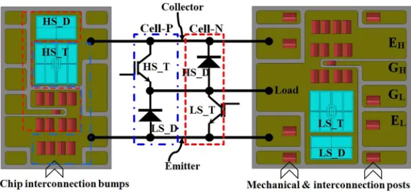
II. SWITCHASSEMBLY 68
The devices used for the switch assemblies are shown in69 Fig. 1:10×9.5×0.07mm3IGBTs and9.5×5.5×0.07mm370 diodes, where the top metallization is treated with NiP/Ag71 finish being solderable. To achieve optimum performance in72 the application, packaging needs to target the integration of the73 positive and negative cells in the HBS (see Fig. 1); this can74 be achieved by having the devices in the same cell soldered75 on separate substrates, which are then mounted, one on top of76 the other, by means of interconnect posts (bumps), as shown in77 Fig. 2. This results in a low stray inductance and double-sided78 cooled power switch, where all devices have their backside in79 direct contact with a cooling surface [1]. Here, both the top and80 bottom substrates are direct bonded copper (DBC) consisting81 of a 1-mm-thick aluminum nitride tile sandwiched by 0.3-mm-82
thick copper on both sides. 83
The chips are soldered to the DBC substrates with 0.1-mm-84 thick Sn–3.5Ag solder alloy. The bumps are Cu with an outside85
IEEE
[image:2.594.150.449.68.209.2]Proof
Fig. 1. Schematic of half-bridge power switch and the corresponding structural view.
Fig. 2. Stacked assembly of substrate–chip–bump–substrate for the HBS. (a) Overall view. (b) Open view.
diameter of 2 mm and length of 3 mm. They are soldered 86
to the front sides of the chips with Sn–3.5Ag solder of 0.1– 87
0.4 mm in thickness, following the shape of the bumps. Due to 88
the reduced thickness of the devices in this case, it is important 89
to understand the effects of different interconnection geome-90
tries, sizes, materials, and shapes to yield optimum reliability. 91
In particular, we report on a comparison of five hollow cylinder 92
(0.5, 0.375, 0.25, 0.125, and 0.0625 mm in wall thickness) 93
copper bumps with solid ones as the interconnect solution (see 94
Fig. 3). 95
III. FE MODELING ANDSIMULATION 96
The developed switch model was characterized electromag-97
netically and electrothermally, employing structural numerical 98
analysis tools [13], and tested for functional performance. 99
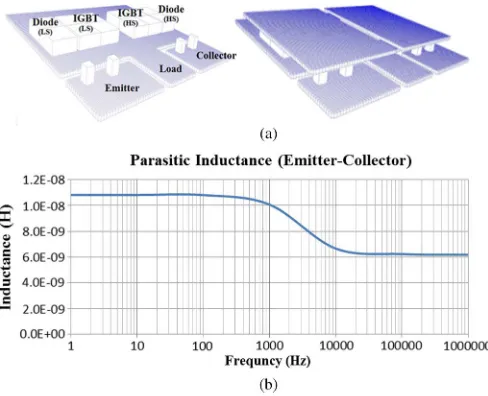
Fig. 4(a) shows the 3-D model mesh for the electromagnetic 100
characterization of the assembly, which was performed with 101
FastHenry [14]. As for the model in Fig. 4, it has been assumed 102
[image:2.594.287.545.241.546.2]that the paths through the chips, solders, and bumps were 103
Fig. 3. Meshing systems used to discretize the assemblies with (a) solid bumps and (b) 0.5-mm-thick hollow bumps.
considered as 5×5×2 mm3 copper filament cubes, which104
carry uniform current and are connected together as a block105 (i.e., two for diode and four for IGBT). The model also uses106 a copper conducting material with an electrical conductivity107 of 59–600–000 S/m. The extraction was taken on a single108 path, while the unnecessary paths were being excluded, so that109 they do not contribute to the measuring path. The values of110 parasitic inductance between all terminal pairs [collector (C),111 emitter (E), and load (L)] were extracted and provided very112 encouraging indications. For instance, the estimated parasitic113 inductance between collector and emitter was less than 7 nH114
above 10 kHz (see Fig. 4). 115
IEEE
[image:3.594.40.284.68.266.2]Proof
Fig. 4. (a) Three-dimensional model for electromagnetic characterization of the module; (b) extracted parasitic inductance.
with thermal cycling [4]. Finite element (FE) thermal and 119
thermomechanical modeling and simulations have been carried 120
out to compare the maximum junction temperature of the 121
chips and the maximum residual stress/creep stain develop-122
ments in the solder joints in the three assembles constructed 123
using the three different bumps. The modeling and simulation 124
were done using commercial FE analysis software ABAQUS 125
6.10-2 and its graphic user interface Complete Abacus 126
Environment. Fig. 3 presents an overview of the meshing AQ2 127
systems consisting of 153–134 and 143–690 C3D8 and C3D6 128
linear brick elements and triangular prism elements to discretize 129
the assembly with solid and 0.5-mm-thick hollow cylinder 130
bumps. Here, the largest element is 1×1×0.45 mm3, and
131
the smallest element is 0.5×0.25×0.025 mm3. In
addi-132
tion, S4 shell elements of 0.5 mm × 0.5 mm or 0.5 mm 133
× 0.25 mm, in size, were also used to discretize the NiP 134
(nickel–phosphorus) finish on the surfaces of the substrates 135
and the Al metallization on two sides of the chips and in-136
cluded in the thermomechanical modeling and simulation. For 137
both diodes and IGBTs, the top side was treated with a gal-138
vanic process consisting of a 3.2 μm/500 nm/300 nm-thick 139
AlSiCu/NiP/Pd solderable metallization, and the back side 140
consists of a1 μm/300nm/300 nm-thick AlTi/Ni/Ag metal-141
lization. However, in the present model, they were assumed 142
as a layer of 3.2-μm-thick Al on the top side and a layer of 143
1-μm-thick Al on the back side of the chips. This is based on the 144
fact that most of the NiP/Pd and Ni/Ag layers would react with 145
the liquid Sn–3.5Ag solder to form intermetallic compounds 146
(IMCs) embedded within the matrix of the solder during the 147
reflow process, and such IMCs were neglected. 148
As shown in Fig. 5, the assembly was first subjected to 149
a predefined temperature profile to simulate the stress and 150
strain development during the reflow process. In this stage, all 151
the solder joints were deactivated, and thus, strain/stress did 152
not develop in them until solidification of the molten solder 153
occurred. Then, power losses of the IGBTs and diodes (see 154
Fig. 6) were taken as heating sources to simulate the thermal 155
performance of the assembly during a realistic mission pro-156
[image:3.594.308.545.69.236.2]Fig. 5. Temperature profile representative of the reflow process.
Fig. 6. Power losses of one IGBT and one diode during a mission profile derived from a real system operation.
Fig. 7. Boundary condition of heat exchange applied in the thermal simulation during the mission profile.
file, and the heat exchange boundary condition, as described157 in Fig. 7, was applied to both the top and bottom cooling158 surfaces of the assembly. The heat exchange coefficient of159 5000 W·m−2·K−1 is a typical value for using a forced-160
convection cooling in power electronics. The temperature field161 obtained from the thermal simulation was used as inputs to sim-162 ulate the further development of stress/strain in the assembly163
during the mission profile. 164
IEEE
Proof
TABLE I
THERMAL ANDMECHANICALPROPERTIES OFSi, AlN CERAMIC LE,AND
NiP FINISH
Fig. 8. Simulated results of temperature distribution in the assembly for 0.5-mm-thick hollow bumps: (a) whole assembly and (b) assembly with the top substrate removed.
Cu and Al, and Anand’s creep model was used to describe 170
the mechanical properties of the Sn–3.5Ag solder alloy. All 171
the mechanical and thermal properties for the Cu, Al, and 172
Sn–3.5Ag were taken from [5] and [6] and are not repeated 173
here. 174
The simulation cases of the three assemblies with the three 175
different bumps were executed on a PC computer with an Intel 176
Pentium Core i7 CPU 976 at 3.20-GHz processor and 8-GB 177
RAM. The running times were about 50 h, for all the cases, 178
to simulate the thermomechanical residual stress/strain devel-179
opments in the assemblies after the reflow process followed by 180
six cycles of the mission profile. 181
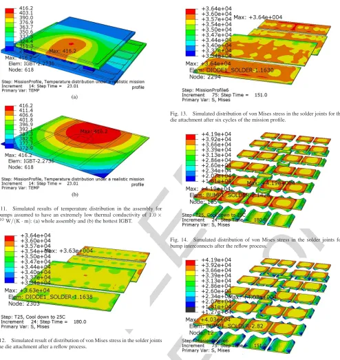
From the simulation results, the highest junction temperature 182
was observed on the IGBT attached on the top substrate and 183
at 23.01 s during the mission profile. Figs. 8 and 9 present the 184
simulated results of temperature distribution in the assembly 185
constructed with the 0.5-mm-thick hollow bumps at 23.01 s 186
during a realistic mission profile, where the bottom chips and 187
substrate of the assembly are separated for observing the hottest 188
IGBT in Fig. 8. Such a result is readily understood because 189
[image:4.594.55.550.74.466.2]the power loss by an IGBT was higher than a diode, and 190
Fig. 9. Simulated temperature distributions in the hottest IGBT of the assem-bly during the mission profile for 0.5-mm-thick hollow bumps.
Fig. 10. Dependence of the simulated highest temperature in the assembly on the wall thickness of the bumps.
the cooling surface of the top substrate was slightly smaller191 than the bottom substrate. The simulated results of temperature192 distribution in the assembly constructed with the other five193 types of bumps were similar, but the highest temperature in the194 hottest IGBT depended on the wall thickness of the bumps (see195 Fig. 10). The highest temperatures in the assembly constructed196 with the six types of bumps increased with decreasing the wall197 thickness of the bumps, and were 16.2◦C–29.3◦C lower than198 the highest temperature in the assembly where the bumps were199 assumed to have an extremely low thermal conductivity of200 1.0×10⁻¹⁰W/(K·m). In all the six cases with real bumps,201
IEEE
[image:5.594.53.547.61.584.2]Proof
[image:5.594.315.534.69.210.2]Fig. 11. Simulated results of temperature distribution in the assembly for the bumps assumed to have an extremely low thermal conductivity of1.0× 10−10W/(K·m): (a) whole assembly and (b) the hottest IGBT.
Fig. 12. Simulated result of distribution of von Mises stress in the solder joints for the die attachment after a reflow process.
Si chips. Furthermore, it is also related to the joining area 217
or the shapes and size of the bumps. This can be seen from 218
the representative simulated results of the assembly with the 219
0.5-mm-thick bumps, as shown in Figs. 12–19. In Figs. 14, 15, 220
18, and 19, the first and last rows of four bump solders are for 221
the two diodes, and the center four rows of bump solders are for 222
the two IGBTs. 223
Figs. 20–23 compare the simulated maximum residual von 224
Mises stress and creep strain accumulation in the solder joints 225
for the die attachment and bump interconnects between the 226
assemblies with the six different bumps. In comparison with the 227
solid bumps, the hollow bumps can reduce the residual stress 228
in the as-reflowed solder joint both for the die attachment and 229
for the bump interconnects (see Figs. 20 and 21). It is noted 230
that the maximum residual stresses in the solder joints for the 231
Fig. 13. Simulated distribution of von Mises stress in the solder joints for the die attachment after six cycles of the mission profile.
Fig. 14. Simulated distribution of von Mises stress in the solder joints for bump interconnects after the reflow process.
Fig. 15. Simulated distribution of von Mises stress in the solder joints for bump interconnects after six cycles of the mission profile.
IEEE
[image:6.594.61.275.66.211.2]Proof
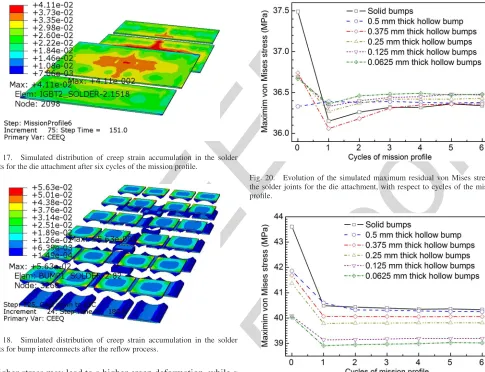
[image:6.594.323.540.67.210.2]Fig. 16. Simulated distribution of creep strain accumulation in the solder joints for the die attachment after the reflow process.
[image:6.594.56.541.251.623.2]Fig. 17. Simulated distribution of creep strain accumulation in the solder joints for the die attachment after six cycles of the mission profile.
Fig. 18. Simulated distribution of creep strain accumulation in the solder joints for bump interconnects after the reflow process.
a higher stress may lead to a higher creep deformation, while a 244
higher creep deformation may result in a larger stress release. 245
During the cooling stage of the reflow, the solder joints for the 246
die attachment in the assembly with the 0.5-mm-thick bumps 247
were probably experienced with relatively large stress release. 248
Therefore, the maximum residual von Mises stress in the solder 249
joints for the bump interconnects still decrease. 250
After some stress release during the first cycle of the mission 251
profile, the maximum residual von Mises stress in the solder 252
joints for the die attachment is almost the same for the six 253
different bumps. The stress release in the assembly with the 254
0.5-mm-thick bumps is negligible, and the stress release in 255
Fig. 19. Simulated distribution of creep strain accumulation in the solder joints for bump interconnects after six cycles of the mission profile.
Fig. 20. Evolution of the simulated maximum residual von Mises stress in the solder joints for the die attachment, with respect to cycles of the mission profile.
Fig. 21. Evolution of the simulated maximum residual von Mises stress in the solder joints for bump interconnects, with respect to cycles of the mission profile.
[image:6.594.292.553.267.631.2]IEEE
[image:7.594.309.542.67.233.2]Proof
Fig. 22. Evolution of the simulated maximum creep strain accumulation in the solder joints for the die attachment, with respect to cycles of the mission profile.
Fig. 23. Evolution of the simulated maximum creep strain accumulation in the solder joins for bump interconnects, with respect to cycles of the mission profile.
Mises stress in the solder joints in the assemblies with the 263
different bumps is quite low. This is due to the fact that there 264
was stress saturation during the creep deformation. 265
In response to the stress release during the first cycle of the 266
mission profile (see Figs. 20 and 21), the maximum creep strain 267
accumulations in the solder joints for both the die attachment 268
and the bump interconnects over this cycle are somewhat lower 269
than those over the other five cycles of the mission profile, 270
which are almost constants (see Figs. 22 and 23). Among 271
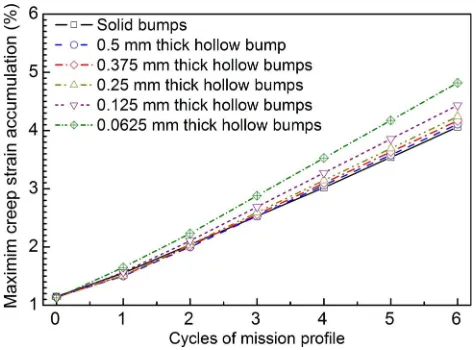
the six assemblies with the six different bumps, the overall 272
maximum creep strain accumulations in the solder joints for 273
the die attachment, with respect to cycles of the mission profile, 274
slightly increase with a decrease in the wall thickness of the 275
bumps. This can be attributed to the fact that the solder joints 276
in the assembly with thinner hollow bumps were subjected to 277
higher temperatures (see Figs. 8 and 10), and the solder alloy 278
has lower creep resistance at higher temperatures. However, 279
the maximum creep strain accumulation in the solder joints 280
for the bump interconnects clearly decrease with a decrease 281
in the wall thickness of the bumps. The 0.5-mm-thick bumps 282
can slightly reduce, and the 0.0625-mm-thick bumps can sig-283
Fig. 24. Lifetimes predicted from the simulated maximum creep strain accu-mulation per cycle for the initiation of fatigue cracks in the solder joints.
nificantly reduce the maximum creep strain accumulation in284 the solder joints for the bump interconnects when compared to285 that for the solid bumps. Such a result reveals that the increase286 in the compliance of the bumps through reduction in the wall287 thickness is more effective than reducing the temperatures288 through an increase in the wall thickness to reduce the creep289 strain accumulation in the solder joints. 290 From the point of view of structural reliability, the reliability291 of the solder joints can be assessed with the creep strain range,292 accumulation, and energy density [5], [8], [9]. In the present293 work, we employ the lifetime model of the SnAgCu solder294 joints based on the creep strain accumulation [9], as follows: 295
Nf = 1
0.0405Δεcr
(1)
where Nf is the lifetime in number of cycles, and Δεcr is296
[image:7.594.44.282.68.243.2]IEEE
[image:8.594.302.552.70.529.2]Proof
Fig. 25. Structure of half-bridge prototype (HBS).
IV. SWITCHPROTOTYPE ANDPRELIMINARY 319
FUNCTIONALTESTING 320
An initial prototype was constructed with the AlN-based 321
substrate available in our laboratory. First the transistor and 322
diode chips are soldered underside (collector and cathode) 323
onto a DBC substrate with a 100-μm-thick Sn–3.5Ag preform 324
that is employed in a fluxless reflow soldering process at a 325
peak temperature of 260◦C for 5 min. Ultrasonically bonded 326
375-μm-thick aluminum wires are used to create the gate and 327
emitter interconnections needed to drive the IGBT. These wires 328
are not power connections but only driving signals. Then, the 329
cylindrical copper bumps are soldered onto the chips using the 330
62Sn36Pb2Ag solder paste reflowed at a peak temperature of 331
240◦C for 5 min. Finally, the two substrates shown in Fig. 25 332
are positioned, one on top of the other, and soldered using 333
the 62Sn36Pd2Ag solder paste at a temperature of 260 ◦C 334
for 5 min. 335
The functionality of the prototype was tested in a basic half-336
bridge dc–ac converter, which can be implemented on typical 337
working conditions of multilevel converters. Fig. 25 shows the 338
structure of the HBS topology, where the top view of the HBS 339
structural halves with the indication of the electrical terminals 340
of HS_D and HS_T, corresponding to the high-side diode and 341
transistor, respectively; LS_D and LS_T relate to the low-side 342
diode and transistor, respectively.EH,GH, andEL,GLare the
343
high- and low-side emitter and gate terminals, respectively. 344
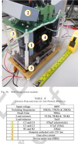
Fig. 26 illustrates the fully integrated prototype assembly, 345
containing two heatsinks, fans, dc-link capacitors, and resistors 346
mounted all together, such that the gate drive is connected at 347
the bottom and the dc-link capacitors and resistors to the top 348
part of the power module. This configuration will not only 349
isolate the gate signals to/from the power circuit but also reduce 350
the external loop inductance of the wires connected to the 351
module where the dc-link capacitors and the gate signals are 352
very close to the devices. The test conditions were set, as 353
depicted in Table II. A fixed dead time of 0.9μs was chosen, 354
and the inverter is tested in an open-loop system. Two identical 355
heatsinks, each embedded with a 12-V fan, were attached to 356
Fig. 26. Half-bridge power module.
TABLE II
DESIGNPARAMETERS OF THEPOWERMODULE
IEEE
[image:9.594.41.549.66.563.2]Proof
Fig. 28. Experimental result: collector–emitter voltage.
with a thermocouple on the device side closer to the IGBT, 376
so that the average heatsink and device temperature can be 377
estimated. 378
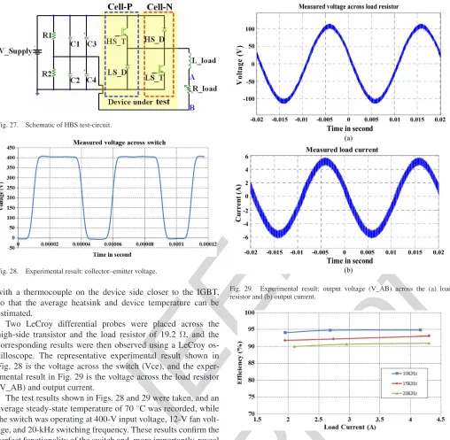
Two LeCroy differential probes were placed across the 379
high-side transistor and the load resistor of 19.2 Ω, and the 380
corresponding results were then observed using a LeCroy os-381
cilloscope. The representative experimental result shown in 382
Fig. 28 is the voltage across the switch (Vce), and the exper-383
imental result in Fig. 29 is the voltage across the load resistor 384
(V_AB) and output current. 385
The test results shown in Figs. 28 and 29 were taken, and an 386
average steady-state temperature of 70◦C was recorded, while 387
the switch was operating at 400-V input voltage, 12-V fan volt-388
age, and 20-kHz switching frequency. These results confirm the 389
perfect functionality of the switch and, more importantly, reveal 390
a very contained value of parasitic inductance, as shown in the 391
graph depicted in Fig. 28. As for the result, it is clear that there 392
is an absence of voltage overshoot across the switch during 393
current commutation. In addition, the result also agrees with 394
the reduced stray inductance extracted by the electromagnetic 395
simulation. 396
The graph shown in Fig. 30 is the calculated efficiency of 397
the converter, using the supply input and experimental results 398
at three different frequencies, as follows: 399
η=Pout
Pin ×100% (2)
Pin =Pin−PR (3)
PR=
2Vin
2
2
R (4)
Fig. 29. Experimental result: output voltage (V_AB) across the (a) load resistor and (b) output current.
Fig. 30. Efficiency as a function of output current at different switching frequencies.
where 400
Pin input power of the overall circuit; 401
Pout output power; 402
Pin converter input power. 403
The total power consumed by the two resistors (R1 and R2404 in Fig. 27) was evaluated using (4) and deducted from the405 measured input power(Pin), which is the power that entered406
into the converter. Then, the efficiency of the converter is407
calculated. 408
[image:9.594.38.287.68.194.2]IEEE
Proof
TABLE III
LOADINDUCTORCOMPARISON
significant costs on the external passive components and make 414
for a smaller package, while reducing the output ripple current. 415
The price list shown in Table III indicates that using almost the 416
same output ripple current of 0.5 A, a 20-kHz switching fre-417
quency operation can reduce the cost of the inductor by almost 418
three times, using 10-kHz frequency operation. In addition, it 419
is worth mentioning that the presented efficiency graph does 420
not include the power consumed by the driver circuit, and it 421
only includes the power semiconductor device losses, input 422
resistance losses, and output inductance losses. 423
V. CONCLUSION ANDOUTLOOK 424
This paper has presented an advanced integration approach 425
for power device packaging, demonstrating the correct elec-426
trical functionality of the half-bridge power switch and its 427
thermal performance. Solid bumps and thicker hollow bumps 428
have better thermal performance than thinner hollow bumps, 429
in terms of reducing the temperatures at the hottest IGBT. 430
However, thinner hollow bumps can reduce the creep strain 431
accumulation in the critical solder joints, as compared to the 432
solid bumps and thicker hollow bumps. As for the thermome-433
chanical simulation results, the 0.0625-mm-thick bumps can 434
significantly reduce the maximum creep strain accumulation in 435
the solder joints for the bump interconnects. For this reason, 436
such results can effectively improve the reliability of the assem-437
bly, and the approach can greatly enhance power density and 438
reduce stray inductance, while enabling double-sided cooling 439
capability. Preliminary experimental results show an interesting 440
advancement of the state of the art, which is represented by the 441
recently proposed sandwich package concepts based on solid 442
bump interconnections and double-sided cooling [10]–[12], in 443
particular by ensuring a more even temperature distribution 444
within the power module and by further reducing parasitic 445
inductance. For future work, it is anticipated to extend this 446
approach to a more advanced scheme while further reducing the 447
stray inductance, improving the reliability of such assemblies 448
and the ability to test with a direct substrate liquid cooling 449
system. 450
REFERENCES 451
[1] A. Solomon and A. Castellazzi, “Application driven integrated design of 452
a half-bridge power switch,” inProc. IEEE ISPSD ICs, San Diego, CA, 453
USA, 2011, pp. 268–271. 454
[2] F. Z. Peng, “Revisit power conversion circuit topologies-recent advances 455
and applications,” inProc. IEEE 6th IPEMC-ECCE Asia, Wuhan, China, 456
May 2009, pp. 188–192. 457
[3] H. R. Chang, J. Bu, G. Kong, and R. Labayen, “300 A 650 V 70 um thin 458
IGBTs with double-sided cooling,” inProc. IEEE ISPSD ICs, San Diego, 459
CA, USA, 2011, pp. 320–323. 460
[4] X. S. Liu, S. Haque, and G.-Q. Lu, “Three-dimensional flip-chip on flex 461
packaging for power electronics applications,”IEEE Trans. Adv. Packag., 462
vol. 24, no. 1, pp. 1–9, Feb. 2001. 463
[5] A. Zeanhet al., “Thermomechanical modelling and reliability study of 464 an IGBT module for an aeronautical application,” inProc. 9th Int. Conf.465
EuroSimE, 2008, pp. 1–7. 466 [6] A. Zeanh, O. Dalverny, M. Karama, and A. Bouzourene, “Lifetime and 467 reliability assessment of AlN substrates used in harsh aeronautic environ- 468 ments power switch modules,”Adv. Mater. Res., vol. 112, pp. 113–127, 469
2010. 470
[7] W. W. Sheng and R. P. Colino,Power Electronic Modules: Design and471
Manufacture. Boca Raton, FL, USA: CRC Press, 2005. 472 [8] P. Solomalalaet al., “Virtual reliability assessment of integrated power 473 switches based on multi-domain simulation approach,” inProc. ESREF, 474
Arcachon, France, 2007, pp. 1343–1348. 475
[9] A. Syed, “Accumulated creep strain and energy density based thermal 476 fatigue life prediction models for SnAgCu solder joints,” inProc. ECTC, 477
Las Vegas, NV, USA, 2004, pp. 737–746. 478
[10] M. Mermet-Guyennet, “New structure of power integrate module,” in 479
Proc. 4th CIPS, Naples, Italy, 2006, pp. 1–6. 480 [11] J.-N. Calata, J.-G. Bai, L. Xingsheng, W. Sihua, and G.-Q. Lu, “Three- 481 dimensional packaging for power semiconductor devices and modules,” 482
IEEE Trans. Adv. Packag., vol. 28, no. 3, pp. 404–412, Aug. 2005. 483 [12] C. Gillot, C. Schaeffer, C. Massit, and L. Meysenc, “Double-sided cooling 484 for high power IGBT modules using flip chip technology,”IEEE Trans.485
Compon. Packag. Technol., vol. 24, no. 4, pp. 698–704, Dec. 2001. 486 [13] [Online]. Available: http://www.3ds.com/products/simulia/abaqus/ 487 AQ3 [14] [Online]. Available: http://www.fastfieldsolvers.com/ 488 AQ4
Adane Kassa Solomonreceived the M.Eng. degree 489 in electrical and electronic engineering in 2011 from 490 The University of Nottingham, Nottingham, U.K., 491 where he is currently working toward the Ph.D. 492
degree. 493
His area of research is advanced packaging and in- 494 tegration solutions for enhanced performance power 495
converters. 496
Jianfeng Lireceived the B.S. degree in mineralogy 497 from Nanjing University, Nanjing, China, in 1991 498 and the M.S. and Ph.D. degrees in materials science 499 from the Shanghai Institute of Ceramics, Chinese 500 Academy of Sciences, Shanghai, China, in 1996 and 501
1999, respectively. 502
In 2008, he joined the Power Electronics Machines 503 and Control Group, The University of Nottingham, 504 Nottingham, U.K., where he is currently a Research 505 Fellow, working in packaging and assembling tech- 506 nologies for the design and development of high- 507 performance and low-cost power electronics. His recent research interests 508 include lead-free solder alloys, transient liquid phase soldering, sintering of Ag 509
nanoparticles, and planar power modules. 510
Alberto Castellazzi is an Associate Professor511 AQ5 of power electronics with The University of 512 Nottingham, Nottingham, U.K. He has been active in 513 power electronics research and development for over 514 15 years and has had extensive collaborations with 515 major European and international industrial research 516 laboratories and groups on publicly and privately 517 funded research projects. He has authored or coau- 518 thored over 100 papers published in peer-reviewed 519 specialist journals and conference proceedings, for 520 which he also regularly acts as a reviewer. His re- 521 search interests include characterization, modeling, application, packaging, and 522
IEEE
Proof
2006, he was appointed as Personal Chair with The University of Nottingham, 539
Nottingham, U.K., where he leads research into power semiconductor devices, 540
power device packaging, reliability, thermal management, power module tech-541
nologies, and power electronic applications. 542
Prof. Johnson is the Director of the Centre for Power Electronics of the 543
Engineering and Physical Sciences Research Council of the U.K., which 544
combines the U.K.’s best academic talent to address the key research challenges 545
underpinning power electronics, and is a member of the Executive for the U.K. AQ6 546