MICROCHIP LASERS: AN INVESTIGATION OF TRANSVERSE
MODE DEFINITION, SPECTRAL SELECTIVITY AND NOVEL
FREQUENCY MODULATION\UP-CONVERSION
TECHNIQUES.
Neil MacKinnon
A Thesis Submitted for the Degree of PhD
at the
University of St Andrews
1994
Full metadata for this item is available in
St Andrews Research Repository
at:
http://research-repository.st-andrews.ac.uk/
Microchip Lasers: An Investigation of
Transverse Mode Definition, Spectral
Selectivity and Novel Frequency
Modulation/Up-conversion Techniques
A Thesis Presented by
Neil MacKinnon, B.Sc.,
in Application for the Degree of
Doctor of Philosophy
ProQuest Number: 10167416
All rights reserved
INFORMATION TO ALL USERS
The quality of this reproduction is dependent upon the quality of the copy submitted.
In the unlikely event that the author did not send a com plete manuscript and there are missing pages, these will be noted. Also, if material had to be removed,
a note will indicate the deletion.
uest
ProQuest 10167416
Published by ProQuest LLO (2017). Copyright of the Dissertation is held by the Author.
All rights reserved.
This work is protected against unauthorized copying under Title 17, United States C ode Microform Edition © ProQuest LLO.
ProQuest LLO.
789 East Eisenhower Parkway P.Q. Box 1346
Declaration
I, Neil MacKinnon, hereby certify that this thesis has been composed by myself, that it is a record of my own work, and that it has not been accepted in partial or complete fulfilment of any other degree or professional qualification.
I was admitted to the Faculty of Science of the University of St. Andrews under Ordinance General No. 12 on the first of October 1990.
In submitting this thesis to the University of St. Andrews I wish access to it to be subject to the following conditions.
For a period of five years from the date of submission the thesis shall be made available for use only with the consent of the Head of School or Chairman of the Department in which the work was carried out.
I understand, however, that the title and abstract of the thesis will be published during this period of restricted access and that after the expiry of this period the thesis will be made available for use in accordance with regulations of the University Library for the time being in force, subject to any copyright in the work not being affected thereby, and a copy of the work may be made and supplied to any bona fide library or research worker.
Neil MacKinnon,
Certificate
I hereby certify that the candidate has fulfiled the conditions of the Resolution and Regulations appropriate to the Degree of Ph.D.
Dr. Bruce D. Sinclair,
Acknowledgements
I am greatly indebted to many people in St. Andrews both in my time here as an undergraduate and as a postgradute. In particular I would like to thank Dr. Bruce Sinclair for his technical assisstance on this project and his boundless enthusiasm.
In addition to my supervisor I would like to acknowledge the following for their assistance in the ruination of my liver over the past three years, having to suffer them in flat 1/172 and a few other things.
Abstract
In this thesis describes experimental and theoretical work is described for a class of solid-state lasers which are classified by the term "microchip". The work presented here may be grouped into two parts. Chapters 2 and 5 describe work directed towards novel frequency modulation and up-conversion and are therefore of a more developmental flavour. The work presented in chapters 3 and 4 are of a more fundamental nature and pertains to transverse mode definition and spectral selectivity in these devices.
In chapter 2 a laser diode array pumped, electro-optically tunable microchip laser is described. Based on the combined gain/non-linear material neodymium doped magnesium oxide lithium niobate (NdiMgOiLiNbOg) tuning of the six oscillating axial modes was achieved at a sensitivity of 8.9 MHz V-i mm. The device operated in a fundamental spatial mode (M^=l.l) at all the incident pump powers used. The incident pump power threshold was 32 mW and the incident pump power slope efficiency was 6.5 %. The maximum output power obtained was 13 mW. From the pump power dependence of the oscillating mode size and the thermal characteristics of the gain material it was postulated that definition of the transverse mode of operation was by a longitudinally distributed positive guiding duct.
pump induced input surface deformation. As expected bulk changes in the refractive index of the gain material were found not to contribute to cavity stability. The LNP output beam was found to propagate with an value of 1.05 at all the pump powers used. The LNP microchip laser was found to operate in a single axial mode up to 20 mW of output power. Above this level the output of the device consisted of the principal mode located under the 1.047 p,m gain bandwidth and a cavity mode located under the 1.055 jim gain bandwidth. It was found that the single frequency performance of the device could be degraded by detuning of the pump radiation away from peak absorption although the overall performance of the device did not show such a marked dependence on gain length.
The single frequency properties of a laser diode pumped LNP device, as a function of gain length, are the subject of chapter 4. The diode pumped LNP device output exhibited the same excellent spatial characteristics of operation as the Titsapphire pumped device. Fourteen milliwatts of single frequency output was obtained. A model, based on spatial dephasing of longitudinal modes, was modified appropriately to predict the single frequency performance of the LNP device as a function of gain length within the resonator. The gain length was controlled by variation of the pump absorption via diode temperature tuning. The discrepancy between the observed results and predicted results was reduced when the effect of a reabsorption loss differential between the 1.047 p,m and 1.055 pm modes was taken into account. The single frequency performance of the device was found to improve markedly at the highest absorption coefficients. This was postulated to be due to a pump density dependent excited state migration mechanism of a form similar to Auger recombination. The migration process manifested itself in the increased damping, over what would be expected from the upper state lifetime of the material, of a spiking train from the device.
Table of Contents
Chapter 1: Introduction
1.1 Historical Perspective
1.2 Compact, Solid-state Visible Laser Sources 1.3 Derivatives and Applications of Diode Pumped
Microchip Lasers References
Chapter 2: An Electro-optically Tunable Neodymium Doped Magnesium Oxide Lithium Niobate (NdrMgOiLiNbOa) Microchip Laser Pumped by a Laser Diode Array
2.1 : Applications of Electro-optically Tunable Devices and Properties of Nd:Mg0:LiNb03
2.2: Crystallographic Orientation of NdrMgOiLiNbOs Device and Analysis of the Linear Electro-optic Effect in LiNbOs
2.3: Thermally Induced Guiding/Confinement of a Gaussian Eigenmode
2.4: Characterisation of the Laser Diode Array Pumped, Electro-optically Tunable, Nd:Mg0:LiNb03
Microchip Laser
2.4.1: Power Characteristics and Spatial Mode of Operation 2.4.2: Spectral Properties of Output and Electro-optical Tunability of Nd:Mg0 :LiNb03 Microchip Laser 2.5: Conclusions and Summary
References
Chapter 3:Cavity Stability Mechanisms and Operating Characteristics of a Lithium Neodymium Tetraphosphate, LiNdP^Oiz, (LNP) Microchip Laser Excited by a Titsapphire Laser
3.1: Properties and Applications of Stoichiometric Laser Gain 46 Materials
3.2: Thermal and Spectroscopic Properties of Lithium Neodymium 48 Tetraphosphate (LNP)
3.3: Performance Characteristics of an LNP Microchip Laser Excited 52 by a Titsapphire Laser
3.4: Conclusions and Summary 67
References 68
Chapter 4:Operating Characteristics and Spectral Behaviour of a Laser 70
Diode Array Pumped, Lithium Neodymium Tetraphosphate , LiNdP4 0i2, (LNP) Microchip Laser
4.1: A Laser Diode Array Pumped LNP Microchip Laser 70 4.2: Modelling of the Single Frequency Characteristics of 73
Microchip Lasers
4.3: Single Frequency Operating Characteristics and Modelling of 86 LNP Microchip Laser
4.4: Conclusions and Summary 96
References 98
Chapter 5:A Laser Diode Array Pumped, Composite Material Microchip 100
Laser for Frequency Up-conversion
5.1: Properties of Neodymium Doped Y ttrium Ortho vanadate 100 5.2: Criteria for Selection of Frequency Doubling Material for 104
Composite Material Microchip Laser
5.3: Frequency Doubling and Physical Properties of Potassium Titanyl 106 Phosphate (KTP)
5.4: Fabrication of Composite Material Microchip Laser Cavity 110 5.5: Characterisation of a Low Pump Power, Lens Coupled, Nd:YV04 116
/KTP Composite Material Device
Microchip Laser
5.7: 130 mW Green Output Power from a Laser Diode Array 140 Pumped Nd:YV04/KTP Composite Material Microchip
Laser
5.8: Conclusions and Summary 142
References 144
Chapter 6:Conclusions and Options for Further Work 146 6.1 : Conclusions and Summary of Work Carried Out 146
6.2 Options for Further Research 149
Chapter 1: Introduction
In this chapter a brief historical perspective of the early development of diode pumped solid-state lasers will be given before the current status of research and application of laser diode pumped microchip lasers is discussed.
Particular emphasis will be given to the generation of coherent, visible light from all solid-state, or holosteric, systems including direct generation from large band-gap II- VI semiconductors, frequency up-conversion of ni-V semiconductor laser diodes and frequency doubling of laser diode pumped solid-state lasers. A perspective will then be given on the new breed of solid-state lasers reported on in this thesis; the microchip laser. The accent will be on the potential for mass-production of such devices, the present status of research and the current realisation of some of the many commercial applications of this device concept. Finally, future avenues of development for this device concept will be outlined as will the contribution of the work presented in this thesis to the evolution of the microchip laser.
Section 1.1: Historical Perspective
The potential use of diode lasers as pump sources was first identified by Newman [1] who demonstrated that 1.06 jam fluorescence in NdiCaWO^ could be excited by 880 nm radiation generated by electron hole recombination in a GaAs light emitting diode (LED). The first lasing action in a diode pumped system was demonstrated by Keyes and Quist [2] at the Lincoln laboratories of the Massachusetts Institute of Technology who used a bank of GaAs diodes to transversely excite a U^+iCaFi laser rod. The diagram below (figure 1.1.1) shows schematically tiie first diode pumped solid-state laser.
All these preliminary experiments were, however, conducted with the diodes and gain media at either liquid nitrogen or liquid helium temperatures but clearly exhibited the
potentialities of diode pumping in producing a laser source of simpler structure and superior performance than in lamp pumped systems.
Silver Block
Pow er L eads
A u -P lated Integrating Cavity
2.613-1/ Laser R adiation
C aF;:U * Rod
Insulating M ount 0.84-y Pum p
Figure 1.1J : Schematic of First Laser Diode Pumped Solid-state Laser. In the Above Figure the Laser Rod is
4 cm Long and 3 mm in Diameter (after [2])
the absorption of Nd^+. The figure below shows the overlap between the emission spectra of a pulsed flashlamp and a laser diode and the absorption profile of 1% Nd:YAG [5].
i
!
§I
< Nd:YAG A bsorption
500 800 TOO BOO
[image:16.613.71.441.109.335.2]«
I
Figure 1.1.2: Emission Spectra of Pulsed Lamp and AlGaAs Laser Diode in Comparison with Absorption Profile of 1 % Nd:YAG (after [5])
The increase in efficiency with laser diode pumping also has the advantage that the waste heat deposited in the solid-state gain material is less and reduces the requirements for active heat sinking. Additional deleterious heat effects such as thermally induced birefringence and catastrophic failure of the laser material are also reduced. Since the early nineteen nineties increasing research and commercial efforts have centred on laser diode pumps as replacements for lamp pumped lasers. The prime stimulus for this move away from lamp pump sources has been the decrease in the unit costs associated with the manufacture and purchase of semiconductor laser diodes. With increasing competition in the marketplace and the collapse of many defence oriented markets, unit cost of $1 per Watt of continuous wave optical radiation is currently available with, in many cases, mounting and packaging costs far out-weighing the costs of the manufacture of the laser diode itself.
All-solid-state lasers, which enjoy the term "holosteric" meaning "wholly solid" to describe them, therefore have a promising future as spatial and spectral purifiers and energy compression devices for laser diode pumps. The increased radiance and
coherence of the output beam from holosteric lasers is more desirable in a number of important applications such as holography, photomedicine, optical storage and micromachining. The upper state lifetime of lasing ions in crystalline hosts is usually much larger than that in semiconductor laser diodes making significant energy storage/extraction possible in solid-state lasers. As will be outlined below in addition to these highly desirable properties the advent of up-conversion or frequency division of laser lines in solid-state gain media, via non-linear optics, has extended the spectral coverage of holosteric lasers from the ultra-violet to the eyesafe region [1-6].
1.2: Compact, Solid-state Visible Laser Sources
The most direct route perhaps to visible coherent radiation will be the use of a semiconductor laser diode itself emitting in the blue-green. To date work in this area has focused on the large band-gap II-VI semiconductors and in particular ZnSe [7,8]. The first successful demonstration of a blue-green laser diode was performed by Haase et al. [7] who achieved pulsed lasing action at 490 nm in ZnSe at 77 K. Continuous wave lasing action in the blue-green in (Zn, Cd) Se/ZnSe multiple quantum well lasers at 100 K was first reported by Jeon et al. [8] in 1991. Since then continued work has focused on attempting to minimise the deleterious thermal problems associated with the poor electrical contacts present in these devices.
AlGalnP semiconductor laser diodes may form the pump source for new vibronic solid-state media such as Cr^+ doped lithium strontium aluminium fluoride (Cr:LiSAF) [10]. To this end Spectra Diode Laboratories (SDL) have developed a half-Watt, C.W., ten emitter array which introduces the possibility of holosteric self- modelocked lasers. Indeed, utilising half-Watt 670 nm laser diodes polarisation coupled such all-solid-state, self-mode-locked CriLiSAF laser have recently been reported [11].
More currently practicable options for producing visible light from laser diodes is to exploit frequency up-conversion of AlGaAs semiconductor laser diode output. AlGaAs III-V semiconductor laser diode technology has the advantage over other laser diodes in that the technology has considerably matured in the last five years. Another stimulus to this approach has been the wealth and breadth of research devoted to the growth and characterisation of non-linear crystals for frequency doubling techniques. The disadvantages of this approach are that in order to achieve reasonable second harmonic powers an external resonant cavity must be utilised to enhance the fundamental flux within the non-linear crystal [12,13]. Such a scheme, as outlined below, has however been used to produce 41 mW of blue (428 nm) C.W. radiation from 140 mW of diode radiation [13].
Coupling — Optics Diode
Laser 428 nm
Output
Potassium Niobate Resonant, Monolithic Ring Doubler
Feedback
Electronic: Detector
Figure 1.2.1: Resonantly Enhanced Second Harmonic Generation of the Output from a GaAlAs Laser Diode Using a Monolithic Ring (after [13])
The above scheme has further drawbacks in that additional drive electronics are needed to keep the frequency of the laser diode locked to that of the external, enhancement cavity. Additionally the non-linear material offering the highest effective non-linear coefficient for blue generation is potassium niobate (KNbOs) which is notoriously difficult to grow, process and coat. The advent of high power AlGaAs M-MOPA (monolithic master oscillator power amplifier) devices offering single frequency diffraction limited near infra-red powers in the one Watt range may to a certain extent obviate the need for resonantly enhanced doubling schemes with the possibility of single pass doubling in KNbOs. However, the blue-green (478 nm) powers generated are still relatively modest (less than 2 mW) and the M-MOPA device is very sensitive to feedback into the power amplifier section of the device
[14].
Perhaps the most commonly used method to generate coherent visible radiation is frequency doubling of diode pumped, near-infrared lasers. Diode pumped, solid-state lasers satisfied long before laser diodes the necessary requirements on coherence, spectral purity, beam brightness and affordability for efficient non-linear conversion. In addition to these highly desirable properties the three most familiar lasing lines possible in neodymium (0.946 (im, 1.064 |im and 1.32 qm) when frequency doubled would give access to the three primary colours (blue, green and red respectively).
eigenpolarisation of the cavity by acting as a temperature sensitive waveplate within the cavity [16] To eliminate these problems the externally resonantly enhanced doubling technique decouples the lasing and the non-linear conversion processes although, as has been outlined above in the consideration of doubled AlGaAs laser diodes, this approach incurs additional cost and complexity. Despite this considerable effort has been given to a monolithic, ring resonant geometry which has successfully generated 29 mW of green light in the non-linear material magnesium doped lithium niobate (MgOiLiNbOs) [12] from a diode pumped ring Nd:YAG laser.
A third recently available option is to combine the lasing properties of the neodymium ion with the non-linear properties of a frequency doubling crystal so as to produce a self-frequency-doubled solid-state laser which may be diode pumped. Two of these materials are lithium niobate co-doped with magnesium oxide and neodymium (NdrMgOiLiNbOs) and neodymium doped yttrium aluminium borate (NdiYAB). Nd:Mg0 :LiNb03 is a material which has been configured for the first time as an electro-optically tunable microchip laser at St. Andrews and characterised in this thesis (chapter 2). Nd:YAB has produced up to 23 mW of green radiation for 400 mW of incident diode pump [17]. However, Nd:YAB suffers from significant reabsorption of the generated green and has to date been difficult and expensive, in comparison with currently available non-linear crystals, to obtain due to growth problems.
The final option for producing coherent visible radiation is via up-conversion processes in fibre lasers [18.19]. However to date up-conversion in fibre lasers has relied on the exploitation of somewhat exotically doped fibres the pulling of which is still very much a virtuoso art and is far from reaching the volume production associated with conventional silica optical fibres. In addition to fabrication difficulties associated with up-conversion fibre lasers alignment of the pump source, which may either be a solid-state laser or diode laser, needs to be accurate to within sub-micron tolerances. Up-conversion in bulk media is yet another route to visible output from diode pumped systems but currently the visible powers obtained are relatively modest
(in the 2 mW range) and usually require liquid helium cooling of the up-conversion media [20].
Clearly coherent, visible light is, at the moment, most desirably obtained from frequency doubled, diode pumped solid-state lasers. For specialist high power uses flashlamp pumping of doubled solid-state lasers is still an option but is increasingly being superseded by diode pumped designs.
1.3: Derivatives and Applications of Diode Pumped Microchip Lasers
Microchip laser was a term first coined by Mooradian to describe a slice of gain material, polished to plane/parallel étalon tolerances, with dielectric mirrors deposited directly on to the gain material surfaces to define a standing wave lasing cavity [21]. Microchip lasers are excited optically and longitudinally, ideally, by AlGaAs semiconductor laser diodes. Microchip lasers are amongst the smallest and cheapest laser designs available and offer in their many forms desirable operating features comparable with larger conventional laser designs. These desirable characteristics and potentialities of microchip lasers form the technical content of this thesis. These features include linearly polarised emission, fundamental spatial mode operation, high power single frequency operation, electro-optically tunability, pulsed operation and frequency manipulation [21]
One of the highly desirable properties of microchip lasers is their amenability to mass production techniques. The following novel method of high volume production has been developed at the Lincoln Laboratories of the Massachusetts Institute of Technology and is outlined schematically below [21].
B
C
D
[image:22.614.109.413.64.317.2]E
Figure 13.1: Five Step Process for Volume
Fabrication of Curved Mirror Microchip Lasers (after [21])
The five step process begins (step A) with a slice of gain material being processed so as to produce a thin wafer of gain material with plane parallel surfaces. Tlie next step (step B) is to scribe the wafer with a grid pattern as shown. Step C involves polishing one surface of the wafer again. During this additional stage of polishing a natural rounding of the polished surface occurs as polishing slurry tends to build up directly underneath the polishing element. The degree of curvature on the re-worked surface is a function of several factors including the grade of slurry being used, the width of the scribe between each device and the force applied during polishing [21]. The wafer is then coated appropriately to form the microresonator (step 4). The wafer is then diced along the direction of the scribes which define the transverse dimensions of the microchip laser (step 5). Using this method of fabrication has the clear advantage that for example one polishing run is sufficient for processing the wafer of gain material in each of the two processing steps. Similarly, with one coating run every device is coated appropriately. In this thesis smaller quantities of microchip lasers were required for the investigative experiments and a more conventional fabrication method was employed. Usually a starting block was sectioned first into a number of blanks which were then mounted on a polishing block and worked simultaneously to
the required thicknesses and tolerances. The finished devices were then coated simultaneously. Although not as novel as the mass production method outlined above the techniques employed by our fabricators clearly indicated the cost effectiveness of the microchip laser approach. A number of components were worked and coated simultaneously and expenditure on the acquisition of these devices was essentially dictated by the cost of polishing runs or coating chamber time.
Since their invention microchip lasers have seen rapid commercialisation especially in the field of optical fibre communications. Particularly important has been the application of an electro-optically tunable microchip laser, operating at 1.32 fxm, to CATV (common antenna television) systems. This particular, composite material microchip laser is shown schematically below.
Nd:YAG Anti-reflecting Lithium Tantalate Gain Section Coatings Non-linear Section
j m Frequency Modulated
K
^
10"»«
Cavity Defining Dielectric Mirrors
Figure 1.3.2: Electro-optically Tunable, Composite Mateiial Microchip Laser( after [221)
i
Such an electro-optically tunable microchip laser enables, via frequency shift keying j (FSK), the transmission of multiple high definition television (HDTV) channels. The | I prime advantage in using the electro-optically tunable microchip laser is the higher itunable device, though based on a single crystal, is the subject of chapter 2 of this thesis.
Yet another commercial exploitation of novel microchip laser designs has been the commercialisation of Q-switched microchip lasers [23], operating at 1.32 |im, as the basis for OTDR (optical time domain reflectometry) machines. The composite material, Q-switched microchip laser is shown diagramatically below.
Nd: Y AG Lithium Tantalate Gain Section Non-linear Section
I
^ --- Q-SwitchedI
[image:24.613.85.431.215.424.2]% ^
I
Figure 133: Electro-optically Q-switched Microchip Laser (after [23])
The LiTaOs non-linear section acts as a voltage controlled output coupler, between surfaces 2 and 3 for the Nd: Y AG gain section between surfaces 1 and 2 [23]. The NdiYAG gain section effectively defines the frequency properties of the device. Surface 1 is coated so as to be highly reflective at the lasing wavelength, surface 2 is coated so as to be 95 % reflective at the lasing wavelengtli and surface 3 is coated so as to be 50 % reflective at the lasing wavelength. The thickness of the gain section (the distance between surfaces 1 and 2) is chosen so as to ensure that only one axial mode is present under the principal gain bandwidth. In the low Q-state the optical thickness of the LiTaOg is adjusted such that the étalon formed by surfaces 2 and 3 becomes highly transmitting for the allowed frequencies defined by surfaces 1 and 2. In the high Q state the étalon is tuned so as to become effectively highly reflecting for the defined frequency of operation of the gain section. Using this approach
Zayhowski et al. have reported single frequency peak power pulses of 25 kW in sub nanosecond pulse durations [23].
Optical time domain reflectometry (OTDR) is a powerful field technique for determining the attenuation on an optical link down its entire length and resolving the length dependence of the attenuation loss [24]. A short, single frequency, high intensity pulse of the appropriate wavelength is launched down the optical fibre under consideration and the backscattered light is recorded as a function of time. The diagram below illustrates a possible backscatter plot from an optical fibre under examination.
Reflected power
Backscatter Reflection / from joint
Light pulse launched into fiber
Fresnel end reflection Fault loss
Faulty region of joint high attenuation ^ Fiber end
Distance from launch
[image:25.614.82.444.270.529.2]Time
Figure 13 A: Testing of the Attenuation of an Optical Fibre Link Using Optical Time Domain Reflectometry (after [24 J)
displays and other fields presently the domain of larger, conventional diode pumped solid-state lasers.
This thesis contributes to the understanding and evolution of the microchip laser. The material presented here consists of both the developmental work associated with the microchip laser and some of its derivatives and experimental work directed towards further understanding of some of the processes involved in the fundamental operating characteristics of the device. In chapter two a laser diode pumped electro-optically tunable microchip laser is described. The electro-optically tunable microchip laser presented in this chapter was the first ever single crystal electro-optically tunable device. The gain material utilised was lithium niobate co-doped with both neodymium and magnesium oxide (NdiMgOiLiNbOg). The work presented in chapter 2 is the first configuration of this novel gain/non-linear material in a microchip laser format [25,26].
Chapters 3 and 4 present material of a somewhat more fundamental flavour although the results obtained therein shed new and important light on how the fundamental operating characteristics of microchip lasers may be turned to the advantage of the device designer. Chapter 3 presents work on the examination of the definition of the transverse mode of operation in lithium neodymium tetraphosphate (LNP) microchip lasers when excited by a titanium doped sapphire laser simulating a laser diode pump source. Chapter 4 outlines the performance of an LNP microchip laser when pumped by a half-Watt laser diode array. More detailed consideration is then given to modelling the single frequency properties of microchip laser with a model based on spatial dephasing of adjacent longitudinal modes. The model is adapted appropriately to ascertain the importance of the gain length within the gain material in defining the spectral purity of the output. Chapter 5 presents perhaps the most exciting developmental work carried out for this thesis. In this chapter the design and performance of a composite material microchip laser for the production of green radiation is described. Potentialities for the scaling of these devices, in terms of output
References
[1] R. Newman, J. Appl. Phys., 34, p. 437, (1963)
[2] R. J. Keyes and T. M. Quist, Appl. Phys. Lett., 4, p. 50, (1964) [3] L. J. Rosenkrantz, J. Appl. Phys., 43, no. 11, p.4603, (1972)
[4] F. W. Ostermeyer, I.E.E.E. J. Quant. Electron., QE-13, no. 1, p. 1, (1977) [5] T. Y. Fan, Lincoln Laboratory Journal, 3, no. 3, p. 415, (1990)
[6] R. Allen, L. Esterowitz, L. Goldberg, J. R. Weller and M. Storm, Electron. Lett., 22, no. 18, p. 947, (1986)
[7] M. A. Haase, J. Qui, J. M. Depuydt and H. Vheng, Appl. Phys. Lett., 59, no. 11, p. 1272, (1991)
[8] H. Jeon, J. Ding, A. V. Nurmikko, H. Luo, N. Samarth and J. Furdyna, Appl. Phys. Lett., 59, no. 11, p. 1293, (1991)
[9] R. S. Geels, D. W. Nam, D. P. Bour, D. W., Treat, D. F. Welch and D. R. Scifres, Paper CM A4, Conference on Lasers and Electro-optics, (CLEO), 1992,
Technical Digest Series,Vol. 11, Optical Society of America, Washington D. C., U. S. A., p. 11
[10] R. S. Geels, D. F. Welch, D. R., Scifres, D. P. Bour, D. W. Treat and R. D.
Bringans, Paper CThQ3, Conference on Lasers and Electro-optics, (CLEO), 1993, Technical Digest Series, Vol. 12, Optical Society of America, Washington D. C., U. S. A., p. 478
[11] R. Mellish, P. W. French, J. R. Taylor, P. J. Delfyett, L. T. Florez, Paper AMDS, Optical Society of America Topical Meeting on Advanced Sohd-State Lasers, Technical Digest, p. 16, 1994
[12] W. J. Kozolovsky, C. D. Nabors and R. L. Byer, I.E.E.E. J. Quant. Electron., QE-24, no. 6, p.913, (1988)
[13] W. J. Kozolovsky, W. Lenth, E. E. Latta, A. Moser and G. L. Bona, Appl. Phys Lett., 56, no. 23, p. 2291, (1990)
[14] R. Waarts, R. Parke, D. Nam, D. Welch, D. Mehuys, R. Lang, S. O' Brien and D. Scifres, Paper CWC2, Conference on Lasers and Electro-optics, (CLEO), 1993, Technical Digest Series, Vol. 12, Optical Society of America, Washington D. C., U. S. A., p. 240
[15] T. Baer, J. Opt. Soc. Am. B, 3, (1986), p. 1175
[16] T. Sasaki, T. Kojima, A. Yokotani, O. Oguri and S. Nakai, Opt. Lett., 16, no. 21, p. 1665,(1991)
[17] J. Bartschke, R. Knappe, C. Becher, B. Beier, K. J. Boiler and R. Wallenstein, Paper ATuD4, Optical Society of America Topical Meeting on Advanced Solid- State Lasers, Technical Digest, p. 22, 1994
[18] D. Piehler, Laser Focus World, Nov. 1993, 30
[19] S. G. Grubb, K. W. Bennet, R. S. Cannon, W. F. Humer, Paper CPD18,
Conference on Lasers and Electro-optics, (CLEO), 1992, Technical Digest Series, Vol. 11, Optical Society of America, Washington D. C., U. S. A., p.35
[20] T.. Herbert, W. P. Risk, R. M. MacFarlane and W. Lenth, Paper WE5, Optical Society of America Topical Meeting on Advanced Solid-State Lasers, Technical Digest, 1990
[21] J. J, Zayhowski, Lincoln Laboratory Journal, 3, no. 3, p. 427, (1990)
[22] J. J. Zayhowski, P. A. Schulz and S. R. Henion, Paper CThR4, Conference on Lasers and Electro-optics, (CLEO), 1993, Technical Digest Series, Vol. 11, Optical Society of America, Washington D. C., U.S.A., p. 484
[23] J. J. Zayhowski,and C, Dill III, Paper CMI7, Conference on Lasers and Electro-optics, (CLEO), 1992, Technical Digest Series, Vol. 11, Optical
Society of America, Washington D. C., U.S.A., p. 54
[24] J. M. Senior, "Optical Fiber Communications", Second Edition, Prentice Hall International Series in Optoelectronics, p. 825
[25] N. MacKinnon, C, J. Nome and B. D. Sinclair, Paper CThS12, Conference on Lasers and Electro-optics, (CLEO), 1993, Technical Digest Series, Vol. 11, Optical Society of America, Washington D. C., U.S.A., p. 496
Chapter 2: An Electro-optically Tunable Neodymium Doped Magnesium Oxide Lithium Niobate (NdiMgOrLiNbOa) Microchip Laser Pumped by a Laser Diode Array.
Introduction
In this chapter the structure and characterisation will be discussed for a single material, laser diode array pumped, electro-optically tunable microchip laser fabricated from lithium niobate co-doped with magnesium oxide and neodymium (Nd:Mg0:LiNb03). We shall first briefly consider the uses for such ultra-compact tunable sources and the specific properties of this material which combines the gain properties of the Nd^+ ion with the non-linear properties of lithium niobate. The relevant analysis of the linear electro-optic effect in LiNbOg is then considered so as to yield a value for the expected electro-optic tuning coefficient of the device. The pump power induced definition of the transverse mode of operation in this material is discussed in comparison with that existing in Nd:YAG microchip lasers. The experimentally obtained operating characteristics of the NdtMgOtLiNbOg device are then described and set in context with other similar devices.
2.1: Applications of Electro-optically Tunable Devices and Properties of NdiMgOzLiNbOg.
Solid-state lasers with the unique property of electro-optically induced frequency agility have two main uses. These are, firstly, frequency modulated optical communications in coherent optical fibre communications via frequency shift keying[ll (FSK) and, secondly, rapid beam pointing [2]. In the first example, frequency shift keying, zeroes and ones are represented by different spectral components in order to convey digital information. The advantage in using FSK techniques in a coherent fibre optic
communication system is that the laser source itself can be modulated directly and consequently unlike amplitude shift keying (ASK) or phase shift keying (PSK) [1] there is no need for an external modulator for the carrier wave. In fibre optic systems using semiconductor laser diodes as the laser source frequency modulation is accomplished by rapid changes in the injection current [1], In the second example fast, one dimensional pointing of a laser beam may be accomplished by the use of a frequency tunable source and a diffraction grating [2]. The rapid, electro-optically induced frequency shift of the laser is translated into positional agility in a time interval very much faster than can be accomplished using mechanical techniques [2]. Clearly an ultra-compact, robust, electro-optically tunable device such as a laser diode pumped tunable microchip laser, of the appropriate output power, would be a useful component in the systems outlined above.
Neodymium doped magnesium oxide lithium niobate (NdiMgOiLiNbOg) is an optically anisotropic, negative uniaxial, solid-state laser material which combines the excellent gain properties of the neodymium ion with the non-linear and electro-optic properties of LiNbOg. The material LiNbOg suffers from photorefractive damage [3], especially at shorter wavelengths [3], though this is ameliorated by the inclusion of around 5% magnesium oxide. The material suffers from fluorescence quenching so the active ion concentration is usually kept usually fairly low (< 0.5%). However despite the presence of fluorescence quenching the material exhibits good lasing characteristics with an upper state lifetime of around 100 qs for 0.2% neodymium concentration [3]. The principal lasing characteristics of Nd:MgO;LiNbOg for the polarisation exhibiting the highest optical gain (i.e. for lasing in a polarisation direction parallel to the crystal c- axis which we shall define as being the Tt-polarised direction) are shown in figure 2.1.1 in comparison with the principal characteristics of Nd doped Y AG.
is observed at a slightly longer wavelength of 1.093 jim though with a stimulated emission cross-section approximately one fourth of that at 1.084 jam.
Material Gem. ( X 10 -19 cm 2) l-fluor. (M^) Active Ion Cone.
Nd:Mg0:LiNb03 1.8 (7C-polarised) 100 0.2%
[image:32.615.127.480.142.454.2]Nd:YAG 3.5 230 1.0%
Figure 2,1.1: Principal Lasing Characteristics of
Nd'MgO'.LiNbOs (after [3]) and principal characteristics ofNd doped Y AG
1
I
I
0
1.00 1.0S 1.10 1.15 1.20
Wavelength (jim)
Figure 2.1.2: Fluorescence Spectrum for c-axis-polarised Emission
However the full-width, half-maximum linewidth of the 1.084 p.m principal transition in Nd:Mg0 :LiNb03 at 3.5 nm is significantly larger than the 1.064 jj,m transition of the Nd^+ ion in the host material Y AG [4] .
We obtained from Crystal Technology a batch of Nd:Mg0 :LiNb03 material with an active ion concentration of approximately 0.2%. The MgO dopant concentration was approximately 5%. With the above active ion concentration the peak absorption of the pump radiation was found to be 0.2 mm’^ at 806 nm. The absorption of the pump radiation for tiie pump polarised along the crystal c-axis may be seen below.
[image:32.615.170.425.249.454.2]0.20-1
0.15-È
E
0.1 0
->
2-o
S
<
0.05-0.00
790 800 810 820
[image:33.615.141.434.62.297.2]Wavelength (nm)
Figure 2.1,3: Pump Absorption in Nd:MgO:LiNhOs Crystal (0.2 % Nd)
Adopting the appropriate conventions pertaining to optically uniaxial crystals [5] the material was cut to provide a starting piece for propagation along the crystal y-axis [5] which would allow laser oscillation on the 1.084 \xm, high gain, 7t-polarised line [3].
2.2 Crystallographic Orientation of NdrMgOiLiNbOs Device and Analysis of the Linear Electro-optic Effect in LiNbOg .
Dielectric z-axis
and Direction of
High Gain
Polarisation
Dielectric x-axis
and Direction of
Low Gain
Polarisation
[image:34.615.145.436.51.351.2]Dielectric y-axis and
Direction of Laser
Emission
Figure 2.2.1: Crystallographic Orientation and Configuration
ofNd:MgO:LiNb03 Microchip Laser.
The polarisation directions and associated refractive indices are best described by the index ellipsoid [5,6].
.2
X y " z" —Y H—^ + —— — 1
n^ n; n; Eqn 2.1
where x, y, z are called the principal dielectric axes and are the directions along which D and E are parallel. The existence of different refractive indices for different rayj- polarised in different directions is a property known as birefringence. The index ellipsoid (Eqn. 2.1) describes fully the properties of propagation in a crystal and the simplest way to consider the effect of an applied electric field is to examine the changes in the constants (l/nj^, (1/Uy)^ and in equation 2.1.
In the presence of an applied electric field equation 2.1 is modified to
4-v^i y
2
V^2 + 4-2 H4 j
yz4-( l ] f 0
«2 XZ4-2 2 \ ^ 5 J <. 6 V
Eqn.2.2 xy = 1
With direct comparison with equation 2.1 and the assumption of zero electric field
2
and
r n r n r n
«2
—2
—2
1^5 ; 1^6/1
= 0v^z y
It can be shown that [5,7] the linear change in the coefficients in equation 2.2 can be described by the equation
3
Eqn. 2.3
where the summation over] uses the convention
j = 1 = x; j = 2 = y: j = 3 = z
where x, y and z are the principal dielectric axes as outlined above and the applied electric field has components Ej, (Ex, Ey and E%.) Equation 2.3 can best be expressed in
matrix form[5,6,7]
J_ n 'v i
1 '
1
0
1 ■ n ^ 6
"ru ri2 ri3~"Ef
= E2
r63 r62 r63 _E3_
where the 6x3 matrix with elements ry is called the electro-optic tensor [5,7]. The form of the electro-optic tensor for LiNbOg is shown below.
Key
PM
I
e
o
o o
o
Zero ElementsNon-zero Elements
Equal Non-zero Elements but of Opposite Sign
[image:36.614.97.475.117.378.2]Equal Non-zero Elements
Figure 222: Form of the Electro-optic Tensor for LiNbOs (after [9J ).
In general in electro-opdc materials the majority of the ry elements are zero as indicated above. In LiNbOg the only non-zero elements are [6]
rgg = 30.8 ; rig = 9.6 ; rog = 6.8 ; rgi = 32.6 pmV*^
and those linked as shown above in figure 2.2.2. Using equation 2.4 and assuming, firstly, that the electric field is applied only in the direction along the dielectric z-axis (Ex = Ey = 0) and secondly the only non-zero elements are the ones listed above we can obtain an electric field modified form of equation 2.1 i.e
-)
X “
4-v^o yy ' +V“ef -f r33Ez z - = 1 Eqn. 2.5
where we now describe Ux and ny as the ordinary refractive indices and n^ as the extraordinary refractive index so as to illustrate the inherent birefringence of the material. We will call a ray, travelling through the material, polarised along the
extraordinary axis the extraordinary ray and when polarised along the ordinary axis an ordinary ray. Consider the term in equation 2.5
1 + rssEz + A y
=> |r33Ez| = A^-i2 e y => !r33Ez| = 2Ane
Eqn. 2.6
from equation 2.6 we have a field dependent change in the extraordinary refractive index equal to
An. = — n&33Ez e 2 ^ Eqn. 2.7 It may be shown that a frequency shift Ad in the longitudinal mode of operation is
induced by a refractive index change within a laser resonator such that
Ad _
D n Eqn. 2.8
Therefore the frequency shift induced by an applied voltage such that E^ = V^/dz is
Ad = n;r33V,
2d, ■D Eqn. 2.9
Where d is the frequency of the ray polarised in the extraordinary diiection .i.e.
D = :~ Eqn. 2.10
where c is the speed of light, in vacuo, and X is the free-space wavelength of the extraordinary ray. Substitution yields the following expression for the magnitude of the field induced frequency shift.
. n:r33Vz
Ad —
Taking ne=2.2 [3] and r33=30 pmV-^ [6] and X,=L084 |im this yields a figure for the tuning sensitivity of
Ad = 10.4 MHz mm
At first sight the units of the tuning coefficient may seem slightly unfamiliai'. However the units merely take into account the separation of the electrodes applying the electiic field to the material. For example, if the electrode separation was 1 mm then the tuning sensitivity would be 10.4 MHz V-i and so on.
2.3: Thermally Induced Guiding/Confinement of a Gaussian Eigenmode
The aim of this section is to outline two mechanisms by which a stable, lowest order, spatial eigenmode may be confined by a radially varying refractive index profile. The first situation to be discussed will be that of a geometrically stable duct [8,9]. The second example to be discussed will be that of a radially symmetric waveguide [9-11]. The thermally induced waveguide structure confinement mechanism is of particular importance as it has been proposed, by Zayhowski, as being tiie strongest mechanism present in defining the transverse mode of operation in NdiYAG microchip lasers [12]. The physical properties of the NdiMgOiLiNbOg are then compared with those of Nd:YAG so as to predict the most likely stability mechanism present in NdiMgOiLiNbOg.
Propagation in a geometrically stable duct depends on a radially varying refractive index profile of the form outlined below.
n(r)=no-kr- Eqn. 2.12
Where n(r) is the refractive index as a function of the radial coordinate
k is a constant defining the transverse dimensions of the duct
no is the refractive index along the centre of the duct
It can be shown [13] that such a refractive index profile can "trap" a lowest order Gaussian eigenmode with a characteristic spot size given by.
œ o = ^ Eqn. 2.13
The physical processes occurring during confinement are straightforward. The total focussing effect along the length of the duct is sufficient to counteract the spreading, by diffraction, of the confined Gaussian beam described by (Og in equation 2.13. Therefore the stronger the focussing power of the duct, which is represented by a larger k value in equation 2.13 then the greater divergence of a tighter Gaussian eigenmode can be counteracted. This mechanism is expressed by equation 2.13 where the confined Gaussian spot size is inversely proportional to the root of k.
However it is worth noting that the approximations used in reaching equation 2.13 insist on a quadratic refractive index form of the type described by equation 2.12 [9-13] and that the dimensions of the confined mode (given by equation 3.5) are dependent on the wavelength of the beam.
The refractive index profile induced in Nd:YAG microchip lasers in fact acts as a weak optical waveguide [9-10]. It can be shown [10-13] that all waveguides have only one guided mode that has no cut-off frequency (that is a free-space wavelength where the mode is unable to propagate in a particular spatial configuration) and also has dimensions larger than those of the guide itself [10,11]. This spatial mode of operation is designated the HEu mode and is the lowest order mode of optical waveguides. In addition to having no cut-off frequency the HEu mode is the only waveguide mode to have a single lobed, quasi-gaussian intensity profile [11]. Therefore Zayhowski, based on his experimental observations proposes that the spatial mode of operation in Nd:YAG microchip lasers is defined by a weakly guiding waveguide and is the HEu guided mode. Zayhowski has also postulated that [12] the dimensions of the oscillating mode, defined by the waveguide, obey the relationship
®osc. P Eqn. 2.14
Where cOosc. is the oscillating mode size and P is the incident pump power. Zayhowski observed that the dimensions of the oscillating mode were also dependent on the average incident pump power rather than the peak incident pump power. Thermal guiding therefore has been shown, by Zayhowski, to be the strongest mechanism involved in the definition of the transverse mode of operation in NdrYAG microchip lasers.
NdrYAG microchip lasers are characterised by two features which are not dissimilar to those present in NdrMgOrLiNbOg. These features are, firstly, that the absorption of the pump power is relatively uniform throughout the length of the device due to the relatively low absorption coefficient for the pump [3]. Secondly, both host materials have positive dn/dT [12,14] which, in the environment described above, would result in a refractive index profile similar to the form shown in equation 2.12. It is highly likely therefore that, given similar pump conditions and reasonable optical parallelism
between the device surfaces, a very similar thermal mechanism is involved in transverse mode definition in Nd:MgO:LiNbOg microchip lasers.
2.4: Characterisation of the Laser-Diode-Array-Pumped, Electro-optically Tunable, Nd:Mg0 :LiNb0 3 Microchip Laser
2.4.1: Power Characteristics and Spatial mode of Operation
The y-cut NdzMgOiLiNbOg material was sectioned so as to provide starting pieces with a crystallographic orientation as outlined in figure 2.2.1. These pieces were then carefully polished down to a nominal thickness of 700 pm to provide devices of high optical parallelism. The optical parallelism of the NdtMgOrLiNbOg device was examined using a Fizeau interferometer as outlined below.
Probe Beam (Collimated HeNe Radiation)
50/50 Beamsplitter Microchip Laser
Imaging Lens
[image:41.614.124.453.364.603.2]CCD Array
Figure 2.4.1: HeNe Based Interferometer for Examination of Optical Parallelism of Nd:MgO .'LiNbOs Microchip Laser
laser should have excellent optical parallelism between the cavity mirrors at all points across the surface of the device. This clearly maximises the amount of the aperture of the device which may be pumped successfully and offers the best possible initial conditions for any pump power induced cavity stability mechanisms. Our NdiMgO-.LiNbOs device was examined in the HeNe based Fizeau interferometer [15] and, as can be seen from figure 2.4.1, the characterised device was quite far from this ideal.
Figure 2.4.2: Equal Optical Thickness Fringes Between the Surfaces of the Characterised Nd.'MgO.'LiNbOj Microchip Laser.
However as can be seen from the above figure the device exhibited an area in which the parallelism of the device was reasonably good. This region is the large bright, nearly circular equal optical thickness fringe which can be seen at the top of the device. The effective radius of curvature of the area characterised by this bright fringe is large. In the direction corresponding to the NdiMgOiLiNbOg c-axis the radius of curvature is 69 m and the orthogonal direction the radius of curvature is slightly smaller at 63 m. The device was pumped, longitudinally in the centre of this bright fringe and it was this area which, as expected, yielded the best performance. Pumping of the microchip laser away from the best area resulted in poorer output beam quality and a higher pump threshold.The input surface of the device was coated so as to be highly transmissive at the pump wavelength (R<10% @ 806 nm) and highly reflective at the lasing
wavelength (R>99.8% @ 1.084 |im). The output surface of the device was coated so as to be moderately reflective at the pump wavelength (R>70% @ 806 nm), so as to double pass the pump radiation in order to increase the overall efficiency of the device, and R=99.7% at the lasing wavelength.
During device design relatively low output coupling was chosen so as to ensure that in these short, low absorption (ccpeak=0.2 mm'^) regimes the incident pump powers needed to reach threshold could be attained by readily available laser diode pump sources. The characteristics of the finished device are summarised below in figure 2.4.2.
HT at 806 nm, HR at 1.084 jam HR at 806 nm, 99.7% R at 1.084 jam
700 nm H
Crystallographic orientation of microchip laser gain material.
Output
Neodymium doped Magnesium
Gold electrodes Oxide
deposited directly Lithium Niobate microchip laser, on sides of device.
Figure 2 A.3: The Active Nd:Mg0:LiNb03 Microchip Laser
used were chosen to mimic, at the input surface of the device, the pump power density produced at the open facet of the laser diode array. The pumping configuration may be seen below.
SDL-2432-4557, Laser diode array (100 jim X 1 \im active A
area).
t
t
Outputf= 8mm f = 6.5 mm ^ Microchip Laser
Figure 24.4: Coupling Optics Used and Longitudinal Pumping Scheme for NdiMgOiLiNbOs Microchip Laser
Using an apertured, scanning photodiode the full width, half-maximum of the pump spot was found to be 110 jim in the plane parallel to the diode junction and 20 jim in the direction perpendicular to the junction. The pumping of the NdiMgOiLiNbOs device was therefore very similar to positioning, with no intervening coupling optics, the microchip laser very close to the active area of the laser diode itself . Direct pumping of microchip lasers in this manner is called "butt"-coupling [4]. This phrase was first used by Zayhowski and co-workers [4], The device was orientated such that the c-axis of the NdiMgOiLiNbO] material was aligned to be parallel to the polarisation of the laser diode emission. This orientation ensured maximum absorption of the pump radiation [3,17-19]. The measured, peak absorption coefficient of the material (a=0.2 mm-^) thus implied that in a double pass through the device approximately 25% of the incident pump power was absorbed in the gain material.
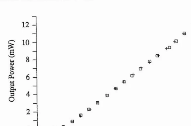
The input power/output power characteristics of the device may be seen in figure 2.4.4. The incident pump power threshold was 32 mW (8 mW absorbed power) and the slope efficiency was, in terms of incident power, 6.5 % (26 % in terms of absorbed power).
The maximum output power achieved was 13 mW. It must be noted that there was no difference in output power in taking the incident pump power from zero up to the maximum and the output power obtained in taking the incident pump power from the maximum used back down to zero.
12
-I
I
O10 -
8 -
6 -
4 -
2
0
-p +a (3
-
-at
a-0 50 100 150 200
[image:45.618.115.443.168.384.2]Incident Pump Power (mW) 250
Figure 2.4.5: Power Characteristics of the Laser Diode Pumped Nd:MgO'.LiNbOg Microchip Laser. Crosses-Input Power "Going Up",
Squares-Input Power "Going Down" "
This lack of "hysteresis" between the two different output curves indicates the absence of any deleterious photorefractive effects [3,17-19]] in the NdiMgOiLiNbOg material over the incident pump powers used. The output of the 1.084 \im emission was found to be polarised very strongly at all pump powers (>20:1) along the Nd:Mg0 :LiNb03 c- axis, or z-axis, in the direction of the highest optical gain [3,17-19]].
Brewster angled plate within the cavity. The lasing fundamental and generated green were therefore in orthogonal polarisations and a type 1, non-critically phase matched, interaction [3] was used utilising temperature tuning of the host material birefringence . This method of phase matching however could not be used in monolithic Nd:MgO:LiNb03 devices where access to the cavity for polarisation selection is of course impossible.
The far-field intensity cross-section, as recorded by a CCD camera, of the 1.084 pm emission can be seen in figure 2.4.6.
Figure 2.4.6: Intensity Cross-section of 1.084 jum Output as seen in the Far-field for (i) Upper Trace: 85 mW of Incident Pump Power
(ii) Lower Trace: 250 mW of Incident Pump Power
Both cross-sections have super-imposed upon them Gaussian fits (points). Clearly there is good agreement between the experimentally obtained intensity profile and that expected from theory. To examine the propagation characteristics of the 1.084 pm output beam the beam was focussed down using a single element lens of 100 mm focal length. An apertured, scanning photodiode was then used to locate and then measure the dimensions of the waist produced by the focussing lens. The divergence of the focussed beam was then calculated from the measured, far-field parameters of the focussed beam. At 85 mW and 250 mW of incident pump power there was to within the experimental uncertainties associated with the experimental technique very little difference between the divergence of the focussed output beam, as measured in the
field, and the divergence of the output beam that would be expected from the size of focussed waist. The corresponding value was found to be 1.1 +/. 9 %. The closely Gaussian intensity profile in the far-field (figure 2.4.6) and the near diffraction limited propagation characteristics of the output beam clearly pointed to the fact that the Nd:MgO:LiNb03 device, at all the incident pump powers used, was operating on a lowest order spatial mode.
With the knowledge that the output beam propagated in a near diffraction limited manner the far-field dimensions of the output beam were used to calculate the dimensions of the oscillating waist within the microresonator of the NdrMgOtLiNbOs device. The oscillating beam waist was found to be dependent on the incident pump power as can be seen in figure 2.4.7. The size of the oscillating waist was found to be dependent on the inverse of the fourth root of the incident pump power as predicted by Zayhowski's model from NdiYAG microchip lasers [12].
100-1
E 9 0 -3
N
I ™1
eu) 60 - c
80-cd 5
0-I
40-40 80 120 160 200 240
[image:47.620.112.450.384.601.2]Average Pump Power Incident on Microchip (mW)
Figure 2.4.7: Fundamental Beam Waist Within Nd:MgO:LiNbOs Microchip Laser's for Filled Squares: Unchopped Pump Open Squares: Chopped Pump .
Fit to Unchopped Pump Results is Power^'"^
postulated by Harkness and Firth [21] as a possible stability mechanism in microchip lasers is gain guiding [21,22]. This is the effect by which the centre of a propagating Gaussian beam is amplified and the edges attenuated by a quadratically varying, radial gain profile so as to produce a fundamental mode size less than that expected by diffraction alone. Any gain related effects present will clearly have a much shorter time constant than any thermal guiding mechanisms. To ascertain the relative contributions, to cavity stability, of long and short time constants respectively the pump beam for the Nd:Mg0 :LiNb03 microchip laser was chopped with a 50% duty cycle at a IkHz repetition rate. The oscillating fundamental waist size was then examined in this chopped pump beam regime. As can be seen in figure 2.4.7 the oscillating waist was found to be dependent on the average incident pump power.
If the definition of the transverse mode of operation was by short term, say gain related, effects alone then the size of the oscillating mode would be dependent on the peak pump intensity. However, as can be seen from the above figure, it is clear that, to within the experimental uncertainty associated with the measurements, the oscillating waist size is dependent on the average incident pump power. Therefore, in this relatively long pump pulse regime thermal effects are predominating over any shorter lived effects in defining the U'ansverse mode of operation. This effect manifested itself in the peak pump power thi'eshold of the device in the chopped regime. The device was pumped slightly away from the optimal area of the device. When the pump beam was chopped with a 50 % duty cycle at 1 kHz the peak pump power threshold of the Nd:Mg0 :LiNb03 device was found to have increased as can be seen in the figure 2.4.8 below.
It is worthwhile now summarising the results on the spatial properties of the output beam. It has been determined that
1. The 1.084 |im output of the device propagates in free space in a near diffraction limited manner with an experimentally determined M- [23] value of 1.1 V. 9 %.
2. The fai’-fieid intensity cross-section, at all pump powers, has an approximately Gaussian shape.
3. The fundamental mode size within the resonator is linearly dependent on the inverse of the fourth root [12] of the incident pump power.
I ::
0 51 4 -O Ow T
-50 100
0 150 200 250
[image:49.618.107.441.205.422.2]Peak Pump Power Incident on Device (mW)
Figure 2.4.8: Peak Pump Power Threshold of Device With Chopped (Filled Squares) and Unchopped (Open Squares) Pump beam
4. In the definition of the U’ansverse mode of operation relatively long time constant thermal effects are predominating over any shorter lived, gain related effects [12,21,22].
Pumping of the microchip laser in areas of non-ideal parallelism, such as the wedged area of the device, resulted in high threshold, poor spatial output characterised invariably by beams with a "comet like" appearance.
2.4.2: Spectral Properties of Output and Electro-optical Tunability of Nd:Mg0 :LiNb0 3 Microchip Laser.
The output spectrum of the NdiMgOiLiNbOa device was examined, using a scanning, plane parallel Fabry-Perot étalon and a i m "Monospek" spectrometer. Even just above threshold the device was operating on six adjacent longitudinal modes, separated by the free spectral range of the microchip cavity, centred around the peak of the high gain, k
or c-polarised, 1.084 pm gain bandwidth [3,17-19]. The oscillating modes at Ppump= 130 mW (incident) can be seen in the transmission of the Fabry-Perot étalon in figure 2.4.9.
Figure 2.4.9: Oscillating Longitudinal Modes ofNd.'MgO.'LiNbOj Microchip Laser.
In the above figure the straight line above the mode groupings is the linear voltage applied to the piezo-driver required to scan the Fabry-Perot étalon. In the tlgure above two free spectral ranges of the étalon are shown. From the above figure the oscillating gain bandwidth of the device was measured to be 430 GHz. The oscillating axial modes were separated by 80 GHz thus implying an optical distance between the cavity mirrors of 680 pm.
Clearly the multi-longitudinal mode operation in this device will somewhat limit the utility of the device for many applications. However, an Nd:Mg0 :LiNb03 microchip laser could be made to be an inherently single-frequency device if the free spectral range of the cavity were reduced so as to ensure the existence of only one cavity mode
beneath the 1.084 pm gain bandwidth. This would entail reducing the thickness of the device to around one fifth of the value used here, i.e. down to approximately 140 pm. To compensate for the reduced absorption of the pump light, because of the much thinner crystal, greater concentrations of the active ion could be introduced into the material. An increase by a factor of five in the neodymium concentration to 1% would compensate for reduced thickness of the device. The upper state lifetime of the active ion would however be reduced by a factor of approximately two [24,25].
[29]. Tuning of a discrete output coupler, hybrid microchip laser has been accomplished by Zhou and Ferguson [30]. In their 1.32 {xm laser-diode-pumped device fine translation of a discrete output coupler, mounted on a piezo-electric actuator was used to modulate the optical length of the cavity. Fifty eight GHz of continuous tuning was observed without polarisation switching [27,30].
In order to monitor the electro-optically induced tunability of an NdiMgOiLiNbOg microchip laser a heterodyne experiment [31] between two laser diode aiTay pumped NdrMgOiLiNbOs devices was performed. One device was electrically connected to a voltage source providing a 120V peak to peak "sawtooth" at 10 Hz. As shown in section 2.2 this voltage was applied, via gold electrodes, transversely across the cavity axis to access the r^] non-linear coefficient in LiNbOs. The remaining control device was left free-running with no applied voltage. Super imposition, to within the bandwidth of the detector (2 GHz), of one cavity mode from each device was achieved by modulation of the pump power applied to each device [32,33].
The frequency sweep of the electrically connected device was found to be 280 MHz. This frequency change corresponds to a tuning sensitivity of 8.9 MHzV'^mm when the electrode separation of 3.78 mm is taken into account,, Additional experiments using a 1 m monochromator indicated that this tuning rate was maintained at higher voltages with 1.7 GHz of tuning having been obtained [34,35]. The frequency sweep of the electrically connected device can be seen in the spectrum analyser printout below. The slight discrepancy between the theoretically calculated tuning sensitivity and that obtained in the heterodyning experiment may be perhaps due to edge effects between the gold electrodes lowering the electric field strength witliin parts of the crystal.
The passive stability of these devices is however an issue. Although less prone to disturbance than external mirror cavities containing air, pump power instability, ambient temperature fluctuations and positional/alignment instability may result in optical thickness changes within the device and thus frequency changes in the device output.
L.
[image:53.617.79.496.63.361.2]CENTER 1 .4 7 0 9 GHz
SPRN'G 00.0 MHz ^
Figure 24.10: Frequency Sweep of the Electrically Connected Nd:MgO:LiNbOs Microchip Laser
Consider again equation 2.8
At) An
D n Eqn. 2.14
Rearranging the above we find that
At) = cAn
A.n Eqn. 2.15
Where c is the speed of light in vacuo, n is the extraordinary refractive index, X is the free space wavelength of operation and An^ is a slight change in the exu'aordinaxy refractive index. Substituting in the appropriate values we find that
At)=L26 x An. Eqn. 2.16
heating of the device would not change the physical length of the device this value would imply, using equation 2.15, a temperature sensitivity of 126 MHz K k Clearly to avoid such long term drift in the frequency of operation of the device temperature stability of the device environment would be of importance. Similarly stability in the intensity of the pump source should be maximised for minimal fluctuations in the frequency of operation [32,33].
The voltage sawtooth applied to the electrically connected device was removed and the two laser diode pumped devices left free-running. Over a ten second interval (the same time interval as the measurement of frequency sweep) the passive frequency drift between the two devices was found to be 22.4 MHz. Taking this drift into account the tuning sensitivity of the NdiMgOiLiNbOg microchip laser can be given as 8.9 MHzV* ^mm +/- 8%. The frequency drift of the two devices relative to one another can be seen in the spectrum analyser printout below.
[image:54.615.81.493.370.606.2]CENTER 1 . ^ 9 1 2 GHz " '... ‘ '
SPftN‘ 2 0 0 . i ' MHz ■'
Figure 2.4.11: Passive Drift ofNd.'MgO.'LiNbOs Microchip Lasers in Heterodyne Experiment
![Figure 1.1.2: Emission Spectra of Pulsed Lamp and AlGaAs Laser Diode in Comparison with Absorption Profile of 1 % Nd:YAG (after [5])](https://thumb-us.123doks.com/thumbv2/123dok_us/8583724.370108/16.613.71.441.109.335/figure-emission-spectra-pulsed-algaas-comparison-absorption-profile.webp)
![Figure 13.1: Five Step Process for Volume Fabrication of Curved Mirror Microchip Lasers (after [21])](https://thumb-us.123doks.com/thumbv2/123dok_us/8583724.370108/22.614.109.413.64.317/figure-process-volume-fabrication-curved-mirror-microchip-lasers.webp)
![Figure 133: Electro-optically Q-switched Microchip Laser(after [23])](https://thumb-us.123doks.com/thumbv2/123dok_us/8583724.370108/24.613.85.431.215.424/figure-electro-optically-q-switched-microchip-laser-after.webp)

![Figure 2,1.1: Principal Lasing Characteristics of Nd'MgO'.LiNbOs (after [3]) and principal characteristics ofNd doped Y AG](https://thumb-us.123doks.com/thumbv2/123dok_us/8583724.370108/32.615.170.425.249.454/figure-principal-lasing-characteristics-linbos-after-principal-characteristics.webp)