A New AC/AC Power Converter
Usman Nasir
[1], Alessandro Costabeber
[2], Patrick Wheeler
[3]and Marco Rivera
[4] [1]-[3]The University of Nottingham, UK[4]Universidad de Talca, Chile [1]Usman.Nasir@nottingham.ac.uk
Abstract— The Future Electrical Network will be based on the integration of different renewable energy sources. In this regard, modular bidirectional power converter architectures will get special attention. Galvanic isolation in such power converter architectures plays a vital role in confining faults. This paper presents a new AC/AC converter concept suitable for Solid State Transformer (SST) applications. The basic operation of the topology is first presented, followed by the development of suitable modulation, commutation and protection methods. The proposed idea is validated in simulation with PLECS.
Keywords—solid state transformer; isolated AC/AC; four-step commutation; isolated matrix converters; cycloconverters
I. INTRODUCTION
Classical matrix converters (MC) offer a single stage high power density conversion solution [1] by avoiding the intermediate DC link stage. As the semiconductor devices directly connect the input to the output of the converter, it is not feasible to employ classical MC in applications requiring galvanic isolation. An example of a system requiring galvanic isolation can be AC transmission or distribution grids [2]. Although line frequency transformers can provide the isolation, they are expensive and bulky in size [3]. However, increasing the operating frequency of the transformer can considerably reduce the cost and size. The operating frequency of the transformer can be increased by utilizing a power converter which modulates the line frequency to a medium or high frequency (MF/HF) waveform, suitable for a MF/HF transformer, and another power converter unfolds the MF/HF waveforms back to low frequency. In literature, this concept has been reported as solid-state transformer (SST) [4, 5] and is illustrated in Fig. 1. SST topologies based on bidirectional switches can provide additional benefits such as reduced footprint and weight.
A single phase to single phase MC based SST, proposed in [6], has limited applications due to the single phase nature of the topology, and to the fact that input and output frequencies must be the same, thus preventing the use of this topology in the interconnection of asynchronous grids. To overcome this problem, a new modular and flexible MC based SST topology has been proposed in [7] and an appropriate modulation, i.e. Venturini Modulation (VM), and commutation techniques were developed.
This paper proposes a new topology based on a different arrangement of bidirectional H bridges, shown in Fig. 2. The figure shows the three-phase to three-phase embodiment, made by simply repeating the three-phase to single-phase version for
each phase. The potential advantages of the proposed topology in SST applications are the lower number of transformers as well as the reduced semiconductor device count meanwhile keeping the modularity intact. Therefore, the proposed SST topology of Fig. 2 offers some additional benefits over the SST topology of [6].
Section II focusses on the operating principle of the proposed SST topology by analyzing and developing an appropriate scalar modulation method. Furthermore, it briefly discusses the commutation technique which is required for a safe operation of the bidirectional H bridges in the converter and also it presents an open circuit fault protection method. Section III presents the key simulation results from PLECS, confirming the correct operation of the converter.
Ph
as
e C
Ph
as
e B
Ph
as
e A
To
Ph
as
e A
N
To
Ph
as
e B
To
Ph
as
e C
N
N
n
n
To Phase A
N To Phase B
To Phase C
N
N
n
To
Ph
as
e A
N To
Ph
as
e B To
Ph
as
e C
N N
n
[image:1.595.320.544.193.272.2]3-Phase Load N
Fig. 2 A new 3-phase to 3-phase isolated AC/AC matrix converter for solid-state transformer applications
Grid Grid
MF/HF Transformer Power
Converter I
Power Converter II
[image:1.595.317.552.463.685.2]II. CONVERTER OPERATION AND ANALYSIS
The three-phase to single-phase version of the proposed SST topology, reported in Fig. 3, is comprised of 4 bidirectional H bridges and one MF/HF isolation unit. Three bridges are at the primary side of the transformer while only one is at the secondary side. Each bridge achieves a four-quadrant operation, with respect to voltage polarity and current direction, at the input and output side. The three cascaded input bridges feed the MF/HF transformer which then connects to the output bridge.
In order to develop a modulation technique for this topology, it is important to briefly discuss the operation of an Indirect Matrix Converter (IMC). In the IMC, the rectifier stage generates a virtual DC voltage which is then modulated, by inverter stage, to generate the required frequency. It is important to mention that the virtual DC voltage is actually the envelop of the three phase input voltages, and therefore at any time instant t the input voltage with the maximum amplitude is selected [8]. A. Modulation Technique
In order to apply a suitable modulation method, the proposed topology can be represented in terms of switching functions which relate output voltage to input voltages. From Fig. 3, the individual bridge voltages at the primary side of the transformer can be represented in (1) – (3). Due to the cascade connection of the three input bridges, the voltage of the transformer can be represented as (4);
[
A1 A2 A1 A2]
A
OA V S S S S
V = − (1)
[
B1 B2 B1 B2]
B
OB V S S S S
V = − (2)
[
C1 C2 C1 C2]
C
OC V S S S S
V = − (3)
[
1 2 1 2]
, , k k k k C B A k k
T V S S S S
V =
−=
(4)
In order to obtain a 50% duty cycle waveform at the transformer, the input bridges moves between the states (5) and (6) with a frequency suitable for the operation of the MF/HF transformer. > > = = = = = = = = = = = = > > = = = = = = = = = = = = > > = = = = = = = = = = = = = B C A C C C C C B B B B A A A A C C B A B C C C C B B B B A A A A B C A B A C C C C B B B B A A A A A T V V V V S S S S S S S S S S S S V V V V V S S S S S S S S S S S S V V V V V S S S S S S S S S S S S V Condition State Voltage V , 0 , 1 1 , 0 1 , 0 , 1 , 0 0 , 1 1 , 0 1 , 0 1 , 0 0 , 1 2 1 2 1 2 2 1 1 2 2 1 1 2 2 1 1 2 1 2 1 2 2 1 1 2 2 1 1 2 2 1 1 2 1 2 1 (5)
It is worth mentioning that the transformer voltage is a “virtual square wave” as it is a function of the square wave of the switching function and of the virtual DC wave as given in (7). Therefore, it contains additional harmonics which must be analyzed to design the complete modulation of the converter.
> > = = = = = = = = = = = = − > > = = = = = = = = = = = = − > > = = = = = = = = = = = = − = B C A C C C C C B B B B A A A A C C B A B C C C C B B B B A A A A B C A B A C C C C B B B B A A A A A T V V V V S S S S S S S S S S S S V V V V V S S S S S S S S S S S S V V V V V S S S S S S S S S S S S V Condition State Voltage V , 1 , 0 1 , 0 1 , 0 , 1 , 0 1 , 0 1 , 0 1 , 0 1 , 0 1 , 0 2 1 2 1 2 2 1 1 2 2 1 1 2 2 1 1 2 1 2 1 2 2 1 1 2 2 1 1 2 2 1 1 2 1 2 1 (6) ) ( ). ( )
(t st V _ t
VT = vir′ dc (7)
The Fourier series of a square wave and a virtual DC wave can be expressed using (8) and (9) respectively:
( )
∞ = = ... 5 , 3 , 1 sin 4 ) ( m s m t m t s ωπ (8)
(n t) b (n t)
a a t V i n n i n n o dc
vir () cos3 ω sin3 ω
1 1 _
∞ = ∞ = + + =′ (9)
The Fourier series of the virtual DC wave in (10) can be calculated by considering Fig. 4. During the interval from π/6
to 5π/6 the input phase ‘A’ will be selected as it has the highest
value than the remaining phases i.e. VA>VBand VA>VC. Note
that when phase ‘A’ is selected, the states of (5) and (6) bypass the remaining phases without disturbing the load current. Therefore, calculating the Fourier series coefficients, such as DC coefficient in (10), the virtual DC wave can be expressed as seen in (11).
= i i dt ta i i
ω π ω π ω π ω 6 5 6
0 32 sin( ). (10)
A1 S A1 S A2 S A2 S B1 S B1 S B2 S B2 S OA V A V C1 S C1 S C2 S C2 S + − B V + − C V + − + − OB V + − OC V + − T V+ − a1 S a1 S a2 S a2 S a V+ − Bidirectional Switch
[image:2.595.314.559.56.209.2]N N N
--
( )
(
)
( )( )
(
)
( )
− −
+ −
− + = ′
∞=
− − − ∞
=
t p p
t n n t
V
i p
p
i n
n
dc
vir p
ω ω
π
3 sin 9 1 1
3 cos 9 1
1 2
1
3 3 ) (
... 5 , 3 , 1
2 4
) 1 ( 3 2 .. 6 , 4 , 2
2 2
_ (11)
The FFT spectrum of the virtual DC wave of Fig. 5, given in (11), has been shown in Fig. 6. The Fourier series of the transformer voltage can be found by substituting (8) and (11) in (7) which will form (12);
( )
( )
(
)
( )( )
(
)
( )
− −
+ −
− +
=
∞=
− − − ∞ = ∞
=
t p p
t n n
m t m t
V
i p
p
i n
n
m
s
T p
ω ω ω
π
3 sin 9 1 1
3 cos 9 1
1 2
1
sin 3 12 ) (
... 5 , 3 , 1
2 4
) 1 ( 3 2 .. 6 , 4 , 2
2 2
... 5 , 3 , 1
2 (12)
It is key to note from Fig. 7 that the input bridges are applying a 50% duty virtual DC enveloped waveform at the transformer. Since the voltage at the transformer is a virtual square wave, with the FFT spectrum of Fig. 8, the transformer design must consider all the harmonic components present in the transformer voltage. Designing the transformer at the switching frequency, by neglecting the harmonic components, can cause core saturation. Hence, the transformer core area must be calculated considering all the harmonic components in the transformer voltage as given in (13).
= V t dt
B N
A .1 T(). max
max (13)
[image:3.595.70.277.67.207.2]Where N is the number of turns, Bmaxis the maximum magnetic flux density of the material and Amaxis the maximum core area required. An active control of the Volt-Second balance across the transformer, such as given in [7], can be added in order to avoid saturation of the core due to undesired DC components
Fig. 4 Illustration of the interval during which input phase ‘A’ will be selected. Voltage in p.u. where the base voltage is Vbase=220V.
-0.9 -0.5 0.0 0.5 0.9 1.4
Vo
ltag
e(
V
)
Angular Position (θ)
VA=sin(θ)
VB=sin(θ+2π/3)
VC=sin(θ+4π/3)
0 π/6 π/3 π/2 2π/3 5π/6 π 7π/6 4π/3 3π/2 5π/3 11π/6 2π
[image:3.595.323.550.72.196.2]VA
Fig. 5 The virtual DC voltage wave. Voltage in p.u. where the base voltage is Vbase=220V.
0 0.2 0.4 0.6 0.8 1 1.2
1.0018 1.0118 1.0218 1.0318 1.0418
Volta
ge
p.u
Time (s)
[image:3.595.321.548.241.378.2]Vvir_dc
Fig. 7 The 50% duty cycle voltage virtual DC enveloped wave at MF/HF transformer with switching component at 5 kHz. Voltage in p.u. where the base voltage is Vbase=220V.
-1.5 -1 -0.5 0 0.5 1 1.5
1 1.002 1.004 1.006 1.008 1.0
V
olta
ge
p.u
Time (s)
VT Fig. 6 Fourier spectrum (FFT) of the virtual DC wave with fundamental, 2nd and 3rd harmonics appearing at 150 Hz, 300 Hz and 450 Hz respectively. p.u. base voltage is Vbase=220V.
0 0.4 0.8 1.2 1.6
0 150 300 450 600 750 900
V
olta
ge
p.u
Frequency (Hz)
Fig. 8 Fourier spectrum (FFT) of the transformer voltage with fundamental of 1.05 p.u magnitude appearing at 5 kHz with side band of 0.13 p.u appearing at 4.850 kHz and 5.150 kHz. p.u. base voltage is Vbase=220V.
0 0.5 1 1.5
0 2.5 5 7.5 10 12.5 15
Volta
ge
p.u
[image:3.595.54.288.246.385.2] [image:3.595.323.548.434.570.2]generated by converter asymmetries – e.g. differences in the turn on/off times of switches, gate driver delays etc. Now, the output voltage can be represented as a function of transformer voltage and the output bridge switches as in (14);
[
a1 a2 a1 a2]
Ta V S S S S
V = − (14)
Similar to the input side state matrix, given in (5) and (6), an output modulation state matrix can also be defined in a way that it unfolds the 50% duty cycle transformer voltage waveform while implementing a sine-wave modulation. The output modulation matrix, which implements a bi-polar PWM, is defined in (15).
< < =
= = =
= = = =
= = = =
+ − +
< < =
= = =
= = = =
= = = =
+ − +
=
1 5 . 0 1 5 . 0
5 . 0 0
0 ,
1
1 ,
0
0 ,
1
5 . 0 0 1 5 . 0
5 . 0 0
0 ,
1
1 ,
0
0 ,
1
2 1 2 1
2 1 2 1
2 1 2 1
2 1 2 1
2 1 2 1
2 1 2 1
D to
D D to to
S S S S
S S S S
S S S S
V V V
D to
to D
D to
S S S S
S S S S
S S S S
V V V
When Interval
State Voltage
V
a a a a
a a a a
a a a a
T T T
a a a a
a a a a
a a a a
T T T
a (15)
The duty cycle Dis obtained using classical sine-triangle or sine-sawtooth comparison. As the output bridge unfolds the transformer voltage, the fundamental component of the output voltage can simply be expressed by (16):
dc vir m
a V V
V = ′. ′ _ (16)
However, the modulating wave needs adjustment to compensate the fact that the virtual DC of (11) contains harmonics and
therefore the actual modulating wave can be expressed using (17).
( )
( )
(
)
(
)
( )
(
)
( )
− − + −
− +
= ′ = ′
∞=
− − − ∞
=
t p
t n n
t V
V V
i p
p
i n
n
o dc
vir m m
p
ω ω
ω π
3 sin 9
1 1 3
cos 9 1
1 2
1
sin 3 3
... 5 , 3 , 1
2 4
) 1 ( 3 2
.. 6 , 4 , 2
2 2 _
(17)
B. Commutation Method
Due to the absence of the free-wheeling path in a bi-directional switch, a suitable commutation strategy must be developed to achieve successful operation of the power converter. The commutation can either be voltage based or current based.
[image:4.595.51.280.71.207.2]In the current based commutation, the output current is sensed and based on its direction, the commutation process is initiated whereas in the voltage based commutation the process is initiated based on the sign of the voltage. Each bidirectional H-bridge commutates independently. Note that voltage at the input and current at the output are at low frequency therefore, it is preferable to use voltage based commutation on the input side bridges and current based commutation on the output side bridge. A case of current based commutation of the output bridge is illustrated in Fig. 11. The shown current based commutation process has four steps and during the process, it is assumed that the current direction doesn’t change.
Fig. 9 Adjusted modulating wave for bipolar sine-triangular PWM. Voltage in p.u. where the base voltage is Vbase=220V.
-1.5 -1 -0.5 0 0.5 1 1.5
1 1.02 1.04 1.06 1.08 1.1
Volta
ge
p.u.
Time (s)
V'm
Fig. 10 Output voltage and output current waveforms at 60Hz as a result of bi-polar sine-wave PWM in the proposed isolated AC/AC SST topology. Voltage in p.u. with base voltage Vbase=220V. Current in p.u. with base current Ibase= 110A
-1.5 -0.5 0.5 1.5
1 1.005 1.01 1.015 1.02
Volta
ge
p.u,
C
ur
re
nt p.u
Time (s)
Va Ia
s7 Iout s0
s1
s6 s2 s3 s5 s4
Iin
IL
[image:4.595.322.544.72.201.2](a) state 1 (b) state 2 (c) state 3 (d) state 4 (e) state 5
[image:4.595.67.505.596.690.2]State 1: The output bridge of the converter is in steady state with s0, s1, s2, s3 turned on. Fig. 11 (a).
State 2: Non-conducting switches s1, s3 can be turned off as
out
I has a path through the antiparallel diodes. Fig. 11 (b).
State 3: The switches s5, s7 can conduct the current in the
direction of Ioutand can be turned on safely. Fig. 11 (c).
State 4: Since s5, s7 are already on, they can provide a path
for Ioutand the switches s0, s2 can be turned off. Fig. 11 (d).
State 5: For the bridge to reach the new steady state, the
switches s4, s6 are turned on. Fig. 11 (e).
It is important to mention that the commutation sequence is designed by utilizing two constraints i.e. voltage source must not short-circuit and current source must not open-circuit. By keeping these constraints in mind, voltage based commutation sequence can also be deduced. In a similar manner, the commutation from active state to a zero state i.e. s0…s3 ON to s2…s7 ON can also be considered.
C. Protection using Clamp Circuit
Although the 4-step commutation sequence presents a safe operation of the converter without open circuiting the current source or short circuiting the voltage source. Practically, it is possible that the measurement of the current direction, gate driver circuit delay, converter asymmetries or control unit malfunction may change the commutation sequence which can interrupt the inductive current path. Depending on the energy present in the inductive load, a voltage spike of corresponding magnitude can pose threat and eventually it can cause permanent damage to the semiconductor devices. Therefore, an overvoltage clamp circuit, which in case of open circuit fault, will provide an alternative path to dissipate the load energy has been designed as shown in Fig. 12. This clamp circuit improves the overall reliability of the proposed topology. The clamp circuit must be sized carefully such that it accommodates the peak inductive load energy without creating dangerous over voltages. Therefore, the load energy can be represented by (18).
2 max
2 1
LI
Eload= (18)
Where Eloadis the load energy,Lis the load inductance and
max
I is the maximum load current. The change in the energy of
the clamp capacitor from its initial to final voltage is given in (19).
) (
2
1 2 2
initial final
clamp CV V
E = − (19)
2 2
2 max
initial final V
V LI C
−
= (20)
During the fault condition, the load energy will be clamped i.e.Eload=Eclamptherefore the size of the capacitor can be
calculated by (20). Note that the resistor sizing can be done based on the application as it will define the speed of energy dissipation in the clamp circuit.Vfinalis the final voltage of the
capacitor and this value must be kept below the voltage rating of the semiconductor devices.
III. SIMULATION RESULTS
A time domain simulation has been done in PLECS Toolbox which validates the theoretical modulation concept developed in the previous section. The following simulation parameters have been used.
SIMULATION PARAMETERS
Parameter Symbol Value
Input voltage Vin 220V AC (peak)
Input frequency fin 50 Hz
Output frequency fo 60 Hz
Switching frequency fsw 5kHz
Output Load
Resistor R 1.9 Ω
Inductor L 1 mH
[image:5.595.321.546.300.535.2]The proposed SST topology has been compared with the topology of [7] in Table II and both topologies use the input bridges to generate a 50% duty ratio MF/HF voltage at the transformer which is then modulated by the output bridge(s). It can be noted that the proposed topology uses a simpler modulation method than that of [7] while offering a reduced number of switches. The traditional MC consisting of 18 semiconductor devices will have the minimum volume in comparison to the other two but it doesn’t provide galvanic isolation whereas the topology of [7] provides galvanic isolation but this comes at the cost of high volume due to increased number of semiconductor devices. However, the proposed
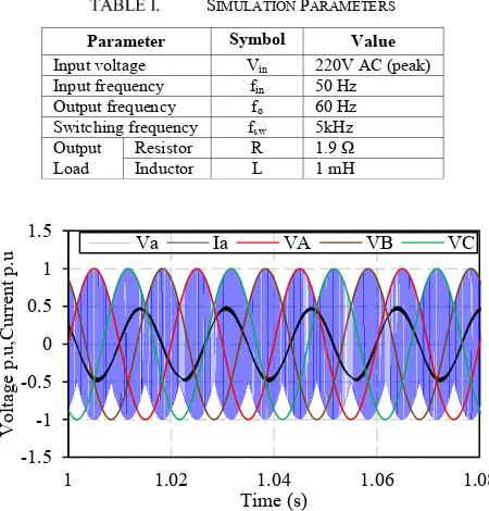
Fig. 13 Input and output voltages and current with fi=50Hz and fo=60Hz in the proposed isolated AC/AC SST topology. Voltage in p.u. with base voltage Vbase=220V. Current in p.u. with base current Ibase= 110A
-1.5 -1 -0.5 0 0.5 1 1.5
1 1.02 1.04 1.06 1.08
Volta
ge
p.u,C
ur
re
nt
p.u
Time (s)
[image:5.595.46.281.525.676.2]Va Ia VA VB VC
topology is assumed to be smaller in volume than [7] due to the reduction in number of devices.
In order to highlight the operation of the clamp circuit, an open circuit fault has been introduced by a sudden shutdown of all the switches in the converter and voltage of the clamp circuit has been monitored as shown in Fig. 15. The initial capacitor voltage is the peak of the virtual DC wave and as soon as the fault occurs, the energy from the inductive load is taken up by the clamp capacitor which will cause a corresponding increase in the voltage until it reaches the final voltage and then the clamp circuit will be discharged based on the value of the resistor connected in parallel to the capacitor.
COMPARISON OF PROPOSED SSTTOPOLOGY,TOPOLOGY OF
[7] AND MATRIX CONVERTER
Parameter Proposed Topology Topology of [7] Converter Matrix
Modulation Method Employed
Sine-triangular PWM
Venturini Modulation
Venturini Modulation
Commutation 4-Step commutation 4-Step commutation 4-Step commutation
Number of
switches 32 48 18
Voltage regulation
ratio 0.5 0.5 0.5
Comparative
volume Medium High Low
Galvanic
Isolation Yes Yes No
CONCLUSION
This paper has discussed a new modular and isolated AC/AC power converter topology which is suitable for grid interconnection systems. The proposed topology extends the concept of indirect matrix converter to the isolated case. Just as
the rectifier stage in the indirect matrix converter generates a virtual DC wave, the input bridges in the proposed topology
generate a virtual square wave. The output bridge can be modulated to generate any desired output voltage and frequency. Furthermore, considering a balanced three phase system, unity voltage regulation ratio can be achieved.
The analysis and operation of the converter concept, including modulation and commutation has been validated in PLECS software.
REFERENCES
[1] P. Wheeler, J. Clare, L. Empringham, M. Apap, and M. Bland,
"Matrix converters," Power Engineering Journal, vol. 16, pp. 273-282, 2002.
[2] F. B. F. Iov, "Advanced power converters for universal and flexible
power management in future electricity network - Converter applications in future European electricity network," University of Nottingham, School of Electrical and Electronic Engineering, University Park, Nottingham2007.
[3] M. D. Manjrekar, R. Kieferndorf, and G. Venkataramanan, "Power
electronic transformers for utility applications," presented at the Industry Applications Conference, 2000. Conference Record of the 2000 IEEE, 2000.
[4] K. Basu, A. Shahani, A. K. Sahoo, and N. Mohan, "A Single-Stage
Solid-State Transformer for PWM AC Drive With Source-Based Commutation
of Leakage Energy," IEEE Transactions on Power Electronics, vol. 30, pp.
1734-1746, 2015.
[5] J. E. Huber and J. W. Kolar, "Solid-State Transformers: On the
Origins and Evolution of Key Concepts," IEEE Industrial Electronics
Magazine, vol. 10, pp. 19-28, 2016.
[6] C. Daolian and L. Lei, "Bi-polarity phase-shifted controlled voltage
mode AC/AC converters with high frequency AC link," in Power Electronics
Specialist Conference, 2003. PESC '03. 2003 IEEE 34th Annual, 2003, pp. 677-682.
[7] U. Nasir, M. Rivera, A. Costabeber, and P. Wheeler, "A Venturini
based modulation technique for a new isolated AC/AC power converter," in
IECON 2016 - 42nd Annual Conference of the IEEE Industrial Electronics Society, 2016, pp. 6243-6248.
[8] L. Tarisciotti, et al., "Modulated Predictive Control for Indirect
Matrix Converter," IEEE Transactions on Industry Applications, vol. PP, pp.
[image:6.595.318.548.95.221.2]1-1, 2017. Fig. 14 Fourrier spectrum (FFT) of the output voltage as a result of
sine-wave PWM with fundamental appearing at 60Hz while switching component appearing at 5 kHz. Voltage in p.u. with base voltage Vbase=220V
0 0.2 0.4 0.6 0.8 1 1.2 1.4
0 2.5 5 7.5 10
Volta
ge
p.u.
Frequency (kHz)
Fig. 15 Clamp circuit in operation due to open circuit fault generated due to sudden shutdown of the converter at t=1.5s. Voltage in p.u. with base voltage Vbase=220V. Current in p.u. with base current Ibase= 55A
-2 -1 0 1 2
1.3 1.4 1.5 1.6 1.7 1.8 1.9 2
Volta
ge
p.u,
C
ur
re
nt p.u
Time (s)
[image:6.595.54.280.98.222.2]