Abstract—This paper proposes a new hybrid MOSFET/ carbon nanotube FET (CNFET) power gating (PG) structure using 32nm technology in the ultra-low voltage region (~0.4V). Traditionally, power gating structure is one of the most effective methods to reduce the power dissipation of systems in sleep mode, but it suffers from increased propagation delay and wake-up time due to the high threshold voltage of power switches in the low voltage region. In this paper, to reduce the propagation delay and wake-up time of the power gating structure while keeping low leakage power in the sleep mode, the CNFET power switches are combined with silicon MOSFET logic-cells. In addition, this hybrid structure reduces the time gap in switching over from silicon MOSFET to CNFET technology. The simulation results of the proposed hybrid power gating at 0.4V are compared to those of the logic blocks without power gating and the MOSFET power gating structure using low threshold voltage power switches, and they show that the proposed hybrid structure reduces the total leakage power by 69.07%, the rush-current by 5.13%, and the delay by 5.96%, on average, compared to the conventional power gating structure for ISCAS85 benchmark circuits designed in 32nm technology; the proposed structure reduces the total leakage by 95.85% at the cost of 3% delay penalty, compared to the logic blocks without power gating for ISCAS85 benchmark circuits designed in 32nm technology.
Index Terms—Carbon Nanotube FET, CNFET, Power Gating, Leakage Power, Sleep Mode
I. INTRODUCTION
S technology scales down to 90nm and below, the bulk CMOS technology has approached the scaling limit due to the increased short-channel effects, increased leakage power dissipation, severe process variations, high power density, and so on. To overcome this scaling limit, different types of materials have been experimented. Si-MOSFET-like Carbon nanotube FET (CNFET) devices have been evaluated as one of the promising replacements in the future nanoscale electronics. The reason that makes CNFETs a promising device is that they have compatibility with high dielectric constant materials and a unique one-dimensional band- structure which restrains back- scattering and which makes near-ballistic operation a realistic possibility; by using this CNFET, a high-k gate oxide can be deployed for lower leakage currents while keeping the on-current drive capability (compared to Si-MOSFET); CNFET has lower
Manuscript received June 06, 2011; revised August 15, 2011.
W.H. Hong is with the School of Electronic Engineering, Daegu University, Gyeongsan, South Korea (e-mail: [email protected]).
K.K. Kim is with the School of Electronic Engineering, Daegu University, Gyeongsan, South Korea (corresponding author to provide phone: +82-53-850-6649; fax: +82-53-850-6619; e-mail: kkkim@ daegu.ac.kr).
short-channel effect and a higher sub-threshold slope than Si-MOSFET [1]-[3].
Despite the recent promising progress of CNFETs, the fabrication of CNT at very large digital circuits on a single substrate has not been achieved. One of the main reasons is the high fabrication cost of CNFETs. Hence, for cost effective utilization of CNFETs and the time-gap reduction in switching over from silicon MOSFET to CNFET technology, the CNFET technology is required to be combined with low cost CMOS technology. Several papers have proposed the hybrid MOSFET/CNFET structure, but the structure is only for simple circuits such as ring oscillator and inverting amplifier [4][5]. Thus, in this paper, we propose a new hybrid MOSFET/CNFET power gating structure which can combine CNFETs with complex silicon MOSFET logic circuits. Power gating (hereafter called PG) structure is one of the most well-known techniques to reduce the sub- threshold leakage in sleep mode where a header and/or footer with high threshold voltage (called sleep transistor) is added between actual power/ground rail and virtual power/ground [6][7]. However, the PG structure is no longer effective in the low voltage region because the high-Vth of the power
switches degrades the operation frequency and increases wake-up time rapidly at the low voltage. As a solution to these issues at the low voltage, in this paper, the MOSFET sleep transistors are replaced by CNFET sleep transistors while MOSFETs are still used for all the cells of logic blocks connected to the sleep transistors. This hybrid technique is very cost-effective and easily implemented, compared to cell-modified hybrid techniques; it is certain that the PG structure is one of the best circuit topologies to which the hybrid MOSFET/CNFET technology can be applied.
The remainder of this paper is organized as follows. Section II shows the concept of the CNFET structure. Section III presents the new PG structure using a CNFET footer. The simulation results are shown in Section IV followed by conclusion in Section V.
II. CARBON NANOTUBE FIELD EFFECT TRANSISTOR
Carbon nanotube FETs employ semiconducting single- wall carbon nanotubes to assemble electronic devices: the single walled CNFET is obtained by replacing the channel of a conventional MOSFET by carbon nantotubes (a one- dimensional conductor obtained by rolling a sheet of graphite) as shown in Fig. 1 [2]. The CNFET device has four terminals (drain, gate, source, and back-gate): a dielectric film is wrapped around a portion of the undoped nanotube in the intrinsic region, and a metal gate surrounds the dielectric; whereas the other nanotube regions are heavily doped for a
Analysis of Power Gating Structure using
CNFET Footer
Woo-Hun Hong, Kyung Ki Kim
(a) (b)
Fig. 1. CNFET structure: (a) Cross sectional view, (b) Top view. 0 200m 400m 600m 800m
VDS(V) 10u
0
IDS
(A
)
VGS
20u 30u
0 V 0.9 V
NMOS CNFET NMOS MOSFET
(a)
VGS(V) 10f
1f
Lo
g
IDS
(A
)
VDS
100f 1p
0.1 V 0.9 V
NMOS CNFET
NMOS MOSFET VDS
0.1 V 0.9 V
-0.5 -0.4 -0.2 0 0.2 0.4 0.5 10p
100p 1n 10n 100n 1u
[image:2.595.50.285.56.168.2](b)
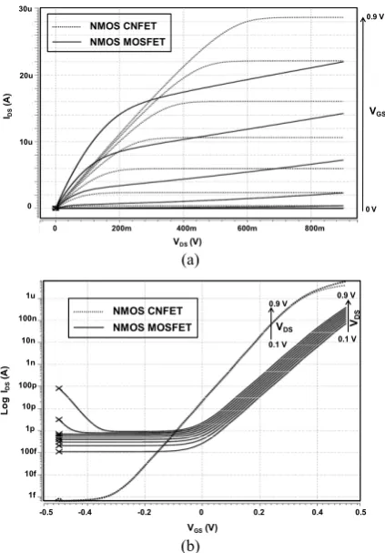
Fig. 2. Drain current of a 32nm N-type CNFET and a 32nm N-type MOSFET as a function of: (a) Drain-to-source voltage for different gate-to-drain voltage, (b) Gate-to-source voltage for different drain- to-source voltage, where the (n,m) of the CNFET is (17,0), the number of nanotubes of the CNFET is 2, the width of the MOSFET is 64nm, the back-gate voltage is 0V, and temperature is 25C.
10u
0
IDS
(A
)
20u 30u
W/ Back gate biasing W/o Back gate biasing
VGS(V)
-0.5 0 0.5 1.0
VBG
0.1 V 0.9 V
VBG=0
40u
3.0n
0 1.0n 2.0n
-0.5 0 0.2
VBG 0.1 V 0.9 V
VBG
=0
VGS (V)
IDS
(A
)
Fig. 3. Drain current of a 32nm N-type CNFET as a function of Gate-to- source voltage for different back-gate voltage, where the (n,m) of the CNFET is (17,0), the number of nanotubes of the CNFET is 2, the width of the MOSFET is 64nm, and temperature is 25C.
low series resistance during the ON-state. As shown in Fig. 1 (a), the top gated CNFETs are fabricated on an oxidized Si-substrate that can be used as a back-gate in the CNFET. In the early 1990s, most CNFETS studied had adopted a back-gate top-contact structure [8][9], in which the nanotubes are grown on a conducting substrate covered by an insulating layer. Two metal contacts are deposited on the nanotube to serve as source and drain electrodes, while the conducting substrate is the gate electrode in this three- terminal device. However, these early CNFETs are found to have poor device characteristics such as an ambipolar transistor characteristic and gentle sub-threshold swing. In order to eliminate the poor device characteristics, dual-gate CNFET structures have proposed. The structures show a MOSFET-like unipolar transistor characteristic, excellent sub-threshold slopes, and a drastically improved OFF state. Each device has one or more single-wall carbon nanotubes which is a semiconductor: the nanotubes can be either a conductor (metal) or a semiconductor according to the angle (represented as a chirality integer vector (n,m)) of the atom arrangement along the nanotube: the nanotube is metallic if (n=m) or (n−m= ‘a multiple of three’), otherwise the tube is semiconducting. The currents of the CNFET device are controlled by adjusting device parameters such as gate length (Lch), the number of nanotubes, chirality vector, and pitch distance between nanotubes [10]. As the gate voltage increases or decreases, the device is electro-statically turned on or off through the gate node. The drain current characteristics of a 32nm N-type CNFET are presented in Fig. 2, where the characteristics are compared to those of the N-type MOSFET. IDS (drain current) of the CNFET is
saturated at higher VDS (drain-to-source voltage) as VGS
(gate-to-source voltage) increases as shown in Fig. 2 (a), where the amount of IDS of the CNFET is greater than that of
the MOSFET although the CNFET width is 6.35nm (5nm of the pitch length and 1.35nm of the diameter) and the MOSFET width is 64nm. According to the simulation result, the device size would be reduced by approximately an order of magnitude when the CNFET is replaced with the MOSFET. In the sub-threshold (weak inversion) region, the characteristics of the CNFET show that IDS of the CNFET is
much greater than that of MOSFET, and that the CNFFET almost does not have Drain-induced barrier lowering (DIBL) and Gate-induced drain leakage (GIDL) effects; whereas the MOSFET has the effects - IDS increases as VDS increases; IDS
can increase at a negative VGS. Figure 2 (b) illustrates IDS
characteristics of the N-type CNFET in the weak inversion region, and shows that the CNFET would be a more practical
solution in the sub-threshold logic design that requires a smaller area than the MOSFET.
Figure 3 shows the back-gate voltage (VBG) impact on the
drain current (IDS) of a 32nm NMOS CNFET; VBG increases
IDS approximately by 30% depending on the top-gate voltage
(VGS). Especially, a small amount of drain current can be
[image:2.595.314.530.456.629.2]Fig. 4. Hybrid power gating structure having a CNFET footer.
Fig. 5. Cross-section of a silicon nMOS with CNFET integration.
III. POWER GATING STRUCTURE USING CNFETFOOTER
This section proposes a new hybrid MOSFET/CNFET PG structure for cost effective utilization of CNFETs. The new hybrid structure solves the low-performance issue caused by high-Vth of the conventional MOSFET PG structure at the
low voltage while keeping low leakage-power dissipation in sleep mode. Figure 4 shows the hybrid PG structure diagram where an N-CNFET (footer) is placed in series to low-Vth
CMOS circuits, and the back-gate node of the N-CNFET is connected to a ground. Figure 5 presents an example of hybrid MOSFET/CNFET integration which is a three-mask optical lithography fabrication process suggested in Ref. [11].
The MOSFET/CNFET PG scheme is the same as the MOSFET PG scheme, but the device parameters of the CNFET footer are different from those of a MOSFET footer. Therefore, the main issue in the hybrid PG structure is to find optimum CNFET device parameters to achieve high speed in active mode and low leakage power in sleep mode. First of all, the optimum threshold voltage should be determined for the speed and leakage power of the PG structure because the current-voltage characteristics of the CNFETS are similar to those of MOSFET as follows [12]:
,
( )
CNFET CNT DD SS th CNT
I n g V V V (1)
where n is the number of nanotubes per device, Vth,CNT is the
threshold voltage, gCNT is the transconductance per nanotube,
and VSS is the voltage drop between the inner source and the
external source node.
In the CNFET device, the channel threshold voltage of the CNFET device can be derived from an inverse function of the diameter of a CNFET as follows [12]:
3
2 3
g th
CNT
E aV
V
e eD
(2)
where Eg is the band-gap energy, and a (~2.49Å) is the
inter-atomic distance between each carbon atom and its
neighbor, V is the carbon - bond energy in the tight
bonding model, e is the unit electron charge, and DCNT is the
carbon nanotube diameter. The diameter is calculated using the following equation [12].
2 2
1 1 2 2
CNT
a n n n n
D
(3) where n1 and n2 are the chirality vector which is represented by the integer pair (n1,n2).
Therefore, the diameter of CNFET, that is, the chirality vector (n1,n2) should be firstly assigned to determine the threshold voltage of CNFET. In addition, the number of nanotubes is another key parameter of the CNFET current according to Eqn. (1). Finally, the pitch distance between nanotubes is the other key parameter due to a screening effect between nanotubes.
As for the leakage power of CNFET, the main leakage component is caused by the band-to-band tunneling (BTBT)
Dependence of Delay & Leakage Power on Chirality Vector (Vth)
Chirality Vector n1 (Vth)
11 (0.499V) 14 (0.392V) 17(0.323V) 20(0.289V) 23(0.250V) 26(0.220V)
Del
ay
(
sec
)
4.6e-10 4.8e-10 5.0e-10 5.2e-10 5.4e-10 5.6e-10 5.8e-10 6.0e-10 6.2e-10
Le
akage Po
wer
(
W
)
0.0 5.0e-9 1.0e-8 1.5e-8 2.0e-8 2.5e-8 Delay
Leakage Power # of nanotubes = 100
Pitch distance = 5nm
(a)
Dependence of Delay & Leakage Power on the number of Nanotube
# of Nanotube
20 40 60 80 100 120 140 160 180 200
Dela
y (
sec)
2e-10 4e-10 6e-10 8e-10 1e-9
Lea
kag
e Po
w
er (
W
)
1.2e-9 1.4e-9 1.6e-9 1.8e-9 2.0e-9 2.2e-9 2.4e-9 2.6e-9
Delay Leakage Current Chirality vector = (17,0)
Pitch distance = 5nm
(b)
Dependence of Delay & Leakage Power on Nanotube Pitch
Pitch (nm)
2 4 6 8 10 12 14 16 18 20
Del
ay (
sec
)
5.2e-10 5.4e-10 5.6e-10 5.8e-10 6.0e-10 6.2e-10 6.4e-10 6.6e-10 6.8e-10
Leak
age Power
(W
)
1.66e-9 1.68e-9 1.70e-9 1.72e-9 1.74e-9 1.76e-9 1.78e-9 1.80e-9 Delay
Leakage Current Chirality vector = (17,0)
# of nanotubes = 100
(c)
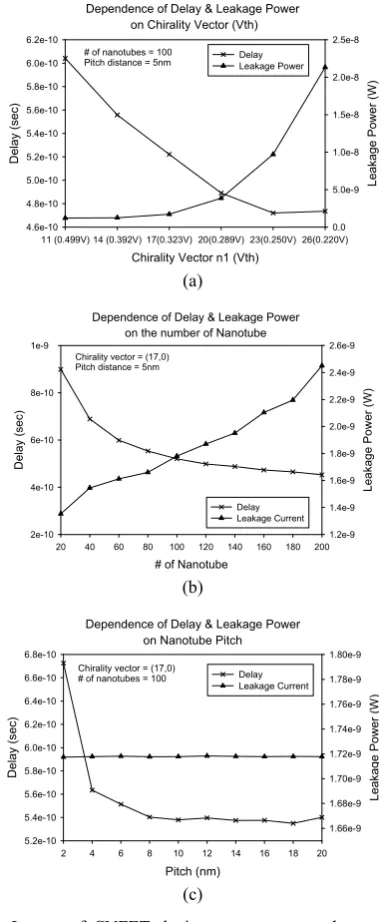
[image:3.595.83.255.187.260.2]mechanism through the semiconducting subbands [13]. In the sub-threshold region, the BTBT current from drain to source becomes significant, and it is also affected by Vth (chirality
vector) and the number of nanotubes. The other leakage currents are relatively small and can be reduced by new techniques such as high-k dielectric material. Figure 6 shows the impact of CNFET device parameters (the chirality vector, the number of nanotubes, and the pitch distance) on the circuit delay and the leakage power in a hybrid PG structure consisting of a CNFET footer and 20 MOSFET inverter chains with each one having 20 inverters using 32nm technology; the chirality vector of the footer is changed from (11,0) to (26,0); the supply voltage is 0.9V, the temperatures are 25C (for leakage measurement) and 125C (for delay measurement). The simulation results show that the delay and leakage power are more affected by the chirality vector and the number of nanotubes than the pitch distance. Especially, the delay-leakage power product significantly increases at around chirality vector (17,0). Also, the product has a minimum value when the number of nanotube is around 100. In order to compare the hybrid PG structure with a MOSFET PG structure, we simulated the same inverter chains using the MOSFET PG structure, whose footer size is 10% of the total NMOS width in the inverter chain. The simulation results present that the delay and leakage power of the MOSFET PG structure are 0.5055nsec and 1.741nW, respectively. From these simulation results, it is demons- trated that the hybrid PG structure can decrease the delay and leakage power of the PG structure even using smaller footer
(about 1% of the total NMOS width in the inverter chain) compared to its MOSFET counterpart.
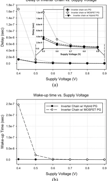
As the power supply voltage decreases below 0.9V, the advantage of the hybrid PG structure becomes clearer. Figure 7(a) presents a simulation result showing the impact of the power supply voltage on the circuit delay of the hybrid PG and MOSFET PG. The simulation results are compared with those of the inverter chains without PG footer. The area over- head of the MOSFET PG is 10% of the total NMOS width, and the area overhead of the hybrid PG is 1% (# of nanotube = 100, pitch=5nm, and chirality vector = (17,0)) of the total NMOS width. As VDD decreases below 0.7V in active mode, the hybrid PG structure becomes more than twice faster than the MOSFET PG structure, and its delay decreases by 70% compared to the MOSFET PG structure at 0.5V. Moreover, the delay of the MOSFET PG structure is exponentially increased at a VDD below 0.6. In addition, as the supply voltage scales down, the wake-up time (sleep-to-active mode transition time) of the MOSFET PG structure significantly increases due to the high threshold voltage of the MOSFET footer, as shown in Fig. 7 (b); whereas the wake-up time of the hybrid PG structure increases a little enough to be negligible, compared to the wake-up time of the MOSFET PG. These simulation results demonstrate that the proposed hybrid MOSFET/CNFET PG structure is very effective in the low voltage region.
IV. SIMULATION RESULTS
The proposed hybrid MOSFET/CNFET PG structure has been implemented and evaluated using ISCAS 85 benchmark circuits designed in 32nm predictive technology model [27] at 0.9V and 0.4V supply voltage. For NMOSFET in the ISCAS85 circuits, a high-k metal gate with Vth0=0.49V and
tox=1.15nm is used; for PMOS in the ISCAS85 circuits, a high-k metal gate with Vth0=−0.49V and tox=1.2nm is used.
For PG footers in the proposed hybrid PG, a 32nm Stanford CNFET HSPICE model [18] has been employed: the chirality vector of the N-CNFET footer is (17,0), and the pitch distance of the N-CNFET footer is 5nm.
In addition, to get more accurate results, a power network model is used: L (bonding/package inductance) is 2nH, R (supply network resistance) is 0.05ohm, and C (supply network capacitance) is 0.05pF. The MOSFET footer size is 10% of the total NMOS width in each original logic block, whereas the size of the CNFET footer is 1% of the total NMOS width. All the simulation results have been measured using random input test vectors at two temperatures (25C for sleep and 125C for active mode).
In order to show the efficiency of the proposed hybrid PG in the ultra-low voltage region, the PG has been evaluated at 0.4V. The leakage power, circuit delay, wake-up time, and rush-current of the proposed hybrid PG structure are normalized by those of the conventional PG structure with low-Vth footers (the high-Vth NMOSFET footers should not
be used due to exponentially increased delay and increased wake-up time at the ultra- low voltage). Also, the leakage power and circuit delay of the proposed hybrid PG are normalized by those of logic blocks without PG structure. As shown in Table I, the simulation results show that the
Delay of Inverter Chain vs. Supply Voltage
Supply Voltage (V)
0.4 0.5 0.6 0.7 0.8 0.9
De
la
y (se
c)
0.0 2.0e-8 4.0e-8 6.0e-8 8.0e-8 1.0e-7 1.2e-7 1.4e-7 1.6e-7 1.8e-7
Supply Voltage (V)
0.5 0.6 0.7 0.8 0.9
Del
ay (
sec)
0.0 2.0e-9 4.0e-9 6.0e-9 8.0e-9 1.0e-8 1.2e-8
Inverter chain w/o PG Inverter chain w/ MOSFET PG
Inverter chain w/ Hybrid PG
(a)
Wake-up time vs. Supply Voltage
Supply Voltage (V)
0.4 0.5 0.6 0.7 0.8 0.9
Wake-up Ti
me (sec
)
0.0 5.0e-8 1.0e-7 1.5e-7 2.0e-7 2.5e-7
Inverter Chain w/ Hybrid PG Inverter Chain w/ MOSFET PG
[image:4.595.71.258.59.374.2](b)
proposed hybrid PG structure reduces the leakage by 69.07%, the delay by 5.96%, the rush-current by 5.13%, and the area by 90% on average for the ISCAS circuits compared to the MOSFET PG structure, whereas the hybrid PG increases the wake-up time by 14.64%. At the ultra-low voltage, the hybrid PG structure yields high performance while reducing the area overhead and keeping low leakage-power dissipation. In the real design situation, the conventional PG structure with low-Vth footers should not be deployed due to increased
leakage power although it would reduce circuit delay compared to the conventional PG with high-Vth footers.
However, the proposed PG structure is imposed a small delay penalty (~3% compared to logic block) in the ultra-low voltage region. The experimental results demonstrate that the proposed hybrid PG structure is very effective and viable in reducing the delay, leakage power, and area overhead of PG structures in the ultra-low voltage region.
V. CONCLUSION
For cost effective utilization of CNFETs, a new PG structure with the CNFET footer has been proposed. This new hybrid scheme makes the PG structure extended to the ultra-low voltage region. The simulation results show that the proposed hybrid PG is a practicable and low-cost solution for high energy reduction in the low voltage nanometer regime. The proposed PG structure would be a practicable solution for low power circuit design with a small delay penalty (~3% compared to logic block) in the ultra-low voltage region.
ACKNOWLEDGMENT
This work was supported by IC Design Education Center(IDEC).
REFERENCES
[1] A. Akturk, G. Pennington, N. Goldsman, “A. Wickenden, Electron Transport and Velocity Oscillations in a Carbon Nanotube,” IEEE Trans. Nanotechnology, Volume 6, Issue 4, pp 469 – 474, July 2007.
[2] H. Hashempour, F. Lombardi, “Device Model for Ballistic CNFETs Using the First Conducting Band,” IEEE Des. Test. Comput., Vol. 25, Issue 2, pp 178-186, March-April 2008. [3] Nishant Patil, Albert Lin, Jie Zhang, H.–S. Philip Wong,
Subhasish Mitra, "Digital VLSI Logic Technology using
Carbon Nanotube FETs: Frequently Asked Questions," IEEE DAC ’09, pp. 304-309, July 26-31, 2009.
[4] F. A. Usmani, M. Hasan, “Novel hybrid CMOS and CNFET inverting amplifier design for area, power, and powermance optimization,” in Proc. IEEE IEDST, pp. 1-5, June 2009. [5] M. Zhang, P. Chan, Y. Chai, Q. Liang, Z. K. Tang, “Novel
local silicon-gate carbon nanotube transistors combining silicion-on-insulator technology for integration,” IEEE Transaction on Nanotechnology, Vol. 8, No. 2, pp. 260-268, March 2009.
[6] M. Anis, S. Areibi and M. Elmasry, "Design and Optimization of Multi-Threshold CMOS (MTCMOS) Circuits," IEEE Tran. on CAD of Integrated Circuits and Systems, Vol. 22, No. 10, pp. 1324-1242, October 2003.
[7] K. Shi and D. Howard, “Challenges in sleep transistor design and implementation in low-power designs,” in Proc. IEEE Design Automation Conf., pp. 113-116, July 2006.
[8] P. L. McEuen, M. S. Fuhrer, and H. Park, “Single-walled carbon nanotube electronics,” IEEE Trans. Nanotechnology, Vol. 1, No. 1, pp. 78-85, Mar. 2002.
[9] P. Avouris, J. Appenzeller, R. Martel, and S. J. Wind, “Carbon nanotube electronics,” Proc. IEEE, Vol. 91, No. 11, pp. 1772 -1784, Nov. 2003.
[10]Stanford University CNFET Model website [Online]. Available: http://nano.stanford.edu /model.php?id=23.
[11]D. Akinwande, S. Yasuda, B. Paul, et. al., “Monolithic integration of CMOS VLSI and CNT for hybrid,” in Proc. Solid-State Device Research Conf., pp. 91-94, Sept. 2008. [12]J. Deng, “Device modeling and circuit performance evaluation
for nanoscale devices: silicon technology beyond 45nm node and carbon nanotube field effect transistors,” Stanford
University, Ph.D Dissertation, Chap 7, 2007.
[13]Ali Jarey, Jing Kong, “Carbon Nanotube Electronics,” Springer, 2009.
TABLEI
SIMULATION RESULTS FOR ISCAS85CIRCUITS WITHOUT PG(VDD=0.4V)
Logic
Normalized by Logic Block (w/o PG)
Normalized by
Conventional PG (with low-Vth NMOSFET footers)
Avg. Leakage
Power Delay Avg. Leakage Power Delay Wakeup Time Rush Current Area
C432 0.049 1.005 0.335 0.981 1.940 0.777 0.1
C499 0.079 1.033 0.500 0.966 1.128 0.944 0.1
C880 0.047 1.028 0.353 0.977 1.132 1.112 0.1
C1355 0.050 1.041 0.271 0.961 1.262 1.272 0.1
C1908 0.030 1.011 0.288 0.990 1.114 0.905 0.1
C2670 0.032 1.041 0.280 0.802 1.063 0.862 0.1
C3540 0.029 1.019 0.221 0.982 0.99 0.845 0.1
C5315 0.035 1.040 0.274 0.981 0.946 0.969 0.1
C6288 0.037 1.047 0.332 0.775 1.143 1.065 0.1
C7552 0.029 1.006 0.238 0.991 0.745 0.735 0.1
Avg.