MODEL 306 PRINTER
MAY 1977
Centronics No. 37400040- Rev. I
CEnTRoniCS
data computer
corp.
MODEL
306
PRINTER
REVISION I
MAY 1977
THE INFORMATION CONTAINED HEREIN IS PROPRIETARY AND IS NOT TO BE RELEASED OR REPRODUCED WITHOUT WRITTEN PER-MISSION OF CENTRONICS data computer corp.
I:EnTROnll:S
data computer corp.
TABLE OF CONTENTS SECTION
11.1
11.2
1.31'.4
1.52.1
2.2
4.1 4.2 4.3 4.4 4.5 4.6 4.7General Description. . . . Logic Flow Diagram. . . . Printer Operation
1.3.1 Character Printing 1.3.2 Paper Movement . . 1.3.3 Special Functions Specifications Summary . Physical Description
SECTION 1 INTRODUCTION
SECTION 2 AND 3
INSTALLATION AND OPERATION
Site Preparation . Shipping Crate. .
Introduction . . . Basic Timing . . . I nitializing the Printer. . 4.3.1 Prime . . . . 4.3.2 Select/Deselect
SECTION 4
THEORY OF OPERATION
Data Input . . . . . 4.4.1 Data Input Timing . 4.4.2 Busy
4.4.3 Decoders. . . . Data Storage . . . .
4.5.1 Timing of Up Counters and Ram Elements. . Character Printing . . . .
4.6.1
I nitiating Printing . . . . 4.6.2 Character Registration and Timing . 4.6.3 Character Generator (ROM)4.6.4 Print Head Operation 4.6.5 Power Driver Circuit Paper Movement . . 4.7.1 Line Feed 4.7.2 Form Feed . 4.7.3 Vertical Tab
4.7.4 Vertical Format Unit (Optional) 4.7.5 Bottom of Form Detection (Optional)
PAGE
1-1
1-2
1-3 1-3 1-4 1-5 1-5 · 1-7/1-82-1
2-2. 4-1
4-1
4-1
4-3
.. 4-3 · . 4··4 4-5 4-5
4-7
.4-10
.4-10.4-12
.4-14 .4-15. 4-21
.4-22
.4-23
TABLE OF CONTENTS (CONT'D)
SECTION PAGE
4.8 4.9 4.10 5.1 5.2 6.1 6.2 6.3 6.4
Special Functions 4.8.1 Bell (Option) 4.8.2 Delete. . . 4.8.3 Paper Empty
4.8.4 Motor Control (Optional) Power Supplies . . . . 4.9.1 +5V Regulator. . . . . 4.9.2 +12 V and -12 V Regulators.
4.9.3 +35 V Power Supply (Unregulated) . LSI Elements Inputs/Outputs. . . .
SECTION 5
.4-30 .4-30 .4-30 · . . . 4-30 .4-30 .4-33 .4-33 . . . . 4-33 · . . . 4-33 . . . 4-37
REMOVAL, REPLACEMENT AND ADJUSTMENT PROCEDURES* Introduction . . . .
Mechanical Assemblies Carriage Mechanism. Platen . . . . Paper Pan
Driving Mechanism Driving Mechanism Idler Pulley Assembly Reed Switch
Printer Base. Frame. . .
. 5-1 . . . 5-1 . . . 5-1 5-4 . 5-5 . . . 5-7 · . 5-9 . . . .5-12
.5-14 · . . . .5-16 · . . . . .5-17 . . . .5-18 -5.2.1 5.2.2 5.2.3 5.2.4 5.2.5 5.2.6 5.2.7 5.2.8 5.2.9 5.2.10 5.2.11 5.2.12 5.2.13 5.2.14 5.2.15 5.2.16 5.2.17 5.2.18 5.2.19 5.2.20 5.2.21
Paper Feed . Pin Feed Unit Ribbon Feed Cover . . . Operator Panel
. . . .5-20
. . . .5-23
Electrical Components Electrical Components Electrical Components
Print Head and Associated Assemblies. Motor Control Assembly Option. . .
Vertical Format Unit (VFU) 63060125-500:~ Option. Printer Drive Mechanism, Model 306 . . . .
SECTION 6 Electrical Adjustment . . . .
Series 300 Preventive Maintenance . Recommended Tools .
Troubleshooting Guide . . .
SECTION 7
· . . . .5-31 · .5-31 . . . 5-32 · . . . 5-32 · . . . 5-33 · .5-33 · .5-37 . . . . 5-38 .5-39
. . 6-1 . 6-1 . . 6-5 6-6
DRAWINGS AND LISTS OF MATERIAILS, ELECTRICAL
A B
SECTION 8
MECHANICAL DRAWINGS AND PARTS LISTS
Logic Board Timing. . . . . Parallel I nterface Specifications .
APPENDICES
LIST OF ILLUSTRATIONS
· A-1 B-1
FIGURE PAGE
1-1 1-2 1-3 1-4 1-5 2-1 4-1 4-2 4-3 4-4 4-5 4-6 4-7 4-8
4-9
4-10 4-11 4-12 4-13 4-14 4-15 4-16 4-17 4-18 4-19 5-1 5-2 5-3 5-4 5-5 5-6 5-7 5-8 5-9 5-10 5-11Model 306 Printer (Top and VFU Covers Removed) Basic Block Diagram
Pri nti ng the Letter (H) Print Head Components Paper Movement Mechanism Printer Dimensions . . . . Model 500 Block Diagram
USASC II Code . . . . .
Data Input Timing . . . . Ti m i ng when Stori ng Data .
Timing of RAM Addressing During Print Cycle
Forward Clutch I nterconnection Diagram. . . .
1-2
'-2
1-3 1-3 1-4 2-1 4-2 4-4 4-6 · 4-11 .4-13 .4-15Block Diagram Character Registration and Timing . . . . . . .4-16
.4-17 .4-20
.4-22
Character Timing. . . .. . . .
DCW Timing, Normal and Elongated Characters . . . . .
Print Head Timing . . . .
Single Line Feed Timing . . . .
Double Line Feed Timing . . . . .
Form Feed and Vertical Tab Timing Schematic - Vertical Format Unit . Timing During Bottom of Form Function
Motor Control Timin~l. . . .
+5V Regulator Interconnection Diagram. .
+12V and -12V Regulator I nterconnection Diagram +35V Unregulated Supply I nterconnection Diagram Carriage Movement Adjustments. . . . Adjustment of Timing Belt . . . .
Adjustment of Timing Belt (View from back of Printer, Forward) Main Motor Belt Adjustment . . . . Bushing End-Play Adjustment for Forward Clutch Shaft, (Preload Clutch)
Location of Drive Pulley Bracket . . . .
Torque Limiting Device (Brake) . . . .
Reed Switch Assembly, Left . . . .
Left Reed Switch Static-Adjustment . . . . Two Adjustment, Paper Feed Mechanism
Adjustment for Paper Holder Gate . . . .
.4-25
.4-26
.4-26
. . .
4-28
.4-29
· .4-32
.4-34
· .4-35
.4-36
LIST OF ILLUSTRATIONS (CONT'D)
FIGURE PAGE
5-14 5-15 5-16 5-17 5-18 5-19 5-20 5-21 5-22 5-23 5-24 5-25 5-26 5-27 5-28 5-29 6-1 6-2 6-3 6-4 6-5 7-1 7-2 7-3 7-4 7-5 7-6 7-7 7-8 7-9 7-10 7-11 7-12 7-13 7-14 7-15 7-16 7-17 8-i 8-1 8-2 8-3 8-4 8-5 8-6 8-7
Locating Dimension for Ribbon Feed Rack . . . " . . . . 5-26 Rack and Pinion Adjustment, Ribbon Mechanism . ., . . . .5-26 Locating Dimension for Left Ribbon Holder Plate with Respect to Rear Guide Bar . 5-27 Locating Dimension for Right Ribbon Holder Plate with Respect to Rear Guide Bar. 5-28 Left Operator and Stopper Adjustment . . . . .
Ribbon Feed Plate and Guide Bar (Left Side). . . . Adjusting Nuts for Right Pawl Operator Movement . . . . Right Pawl Operator Starting Position. . . . Pawl, Ratchet and Cam Movement . . . .. . . Spur on Left Releaser (A L-174) and Roller (A L-146) . Establishing Timing Fence Location and Parallelism
Fence Adjustment and Optics Housing . . . . .
Vertical and Horizontal Alignment of Single Track Optics Housing Motor Control Location and Installation. . . . Paper Tape Reader Adjustment . . . . Location of Subassemblies/Parts by Figure or Symbol Reference Carriage Assembly and Timing Fence
Paper Feed Assembly . . "
Ribbon Feed Assembly . " . . .
Idler and Ribbon Feed Drive . . . .
Drive Assembly . . . . " . . . . Schematic Diagram, Logic/Power Supply Board, 300/fiOO Series . Schematic Diagram, Power Driver Board (Sheet 1 of 2t . . .
Schematic Diagram, Power Driver Board (Sheet 2 of 2t . . . Schematic Diagram, Video Amplifier . . . . Schematic Diagram, I nterconnection Diagram, Connector Card Schematic Diagram, Multitap 50/60 Hz Transformer . . Wiring Diagram, Printer Mechanism. . . . Schematic Diagram, Elapsed Timing Indicator (Option) . . . Logic/Power Supply Board Connections. . . .
PC Board Assembly, Logic/Power Supply Board, 300/S00 Series (Sheet 1 of 2) . PC Board Assembly, Logic/Power Supply Board, 300/S00 Series (Sheet 2 of 2) . PC Board Assembly, Power Driver Board
PC Board Assembly, Video Amplifier . . . . PC Board Assembly, Connector Card . . . . PC Board Assembly, Elapsed Time Indicator (Option)
Cable Assembly, Data Input . . . .
Cable Assembly, Computer I nput Cable (W2) Model 306 Subassemblies
Carriage - AA . . . . Platen - AB . . . . Paper Pan - AC . . . . Driving Mechanism (Part 1 ) - AD Driving Mechanism (Part 2) - AE . Idler Pulley - AF
Reed Switch - AG . . . .
iv
. . 5-28 · .5-29 .5-29 · .5-30 .5-30 · .5-31
· .5-35
· .5-36 .5-36 · .5-37 .5-39 .5-40 6-3 6-4 6-4
· . 6-5
6-5
· 7-3/7-4 · 7-5 7-6 7-7 · . 7-8 · . 7-9 .7-10 · 7-11 .7-12 · 7-13 · .7-14 · 7-19 · 7-21 .7-23 .7-25 · .7-29 · 7-31 · 8-3 · 8-5 · 8-7 8-9 .8-11 · .8-13
LIST OF ILLUSTRATIONS (CONT'D)
FIGURE
8-8 8-9 8-'10 8-11 8-12 8-13 8-14 8-15 8-16 8-17 8-18 8-119 8-20
Base -AH
FrCllme - AI Paper Feed - AJ
Pin Feed Assembly and Paper Drive Shaft Ribbon Feed - AL (Part 1 of 2)
Ribbon Feed - AL (Part 2 of 2) Cover - AM . . . .
Operator Panel - AN . . . .
Multitap Transformer and Electrical Components (Part 1 of 3) - AO Electrical Components (Part 2 of 3) - AP
Electrical Components (Part 3 of 3) - AQ Print Head and Associated Assemblies.
Vertical Format Unit (Option) . . . .
NOTE
Refer to the Engineering Change Notice (ECN) sheets shipped with the printer for changes made to the prin-ter which have not yet been incorporated into the draw-ings in this technical manual. Always keep these Engin-eering Change Notice sheets with the manual.
Revision level indications at the lower right-hand corner of a page reflect at what revision of the manual that page was updated.
PAGE
.8-19 .8-21 .8-23 .8-25 .8-2"1 .8-28 .8-31 .8-33 .8-35 .8-37 .8-39
.8-41
SECTION 1
INTRODUCTION
This manual describes the Model 306 printer, manufactured by Centronics Data Computer Corp-oration. It provides general information, detailed theory of operation and maintenance information enabling field service personnel to service the printer. For serial input or other detailed interface information, a separate document for each interface is published for your reference.
The manual is subdivided into eight sections, each with its specific purpose.
SECTION 1
SECTION 2
SECT10N
3
SECTION
4
SECTION
5
SECTION 6
SECTION 7
SECTION a
APPENDIX
INTRODUCTION, introduces the reader to the scope and content of the manual, and provides the reader with a general description of the printer.
INSTALLATION, contains unpacking and installation instructions for the printer.
OPE RATION, describes the use of alt operator controls and indicators.
THEORY OF OPERATION, contains a detailed description of each major operation performed by the printer electronics, including flow charts, timing diagrams and circuit diagrams.
REMOVAL, REPLACEMENT AND ADJUSTMENT PROCEDURES, includes step-by-step removal and replacement procedures for all major assembl ies and sub-assemblies in the printer.
MAl NTENANCE, includes electrical adjustments, preventive maintenance proc-edures, and a troubleshooting guide.
ELECTRICAL DRAWINGS AND LIST OF MATERIALS, contains a complete set of schematic, wiring and component board layout diagrams and their assoc-iated list of materials for the electrical portion of the printer.
MECHANICAL DRAWINGS AND PARTS LISTS, includes all printer assembly drawings and their associated part lists for the mechanical portion of the printer.
(A) Logic Board Timing (B) Parallel Interface Timing
1.1 GENERAL DESCRIPTION (Figure 1-1)
The Model 306 printer is
a
medium speed impact printer which uses a standard 5 x 7 or optional9 x 7 dot matrix for character generation.
The unit prints at a rate of 120 characters per second, which is approximately one full
aO-chara-cter line per second (including carriage return time). Paper is sprocket-fed, and paper widths from 4
inches to 9% inches (10.2 cm -24.1
~m)
can be accommodated. The printer can produce one original and fourFigure 1-1. MODEL 306 PRINTER (TOP AND VFU COVERS REMOVED)
1.2 LOGIC FLOW DIAGRAM (Figure 1-2)
The standard printer contains an 80-character buffer. For serial data inputs, optional serial interfaces allow,data to be received at rates from 100 to 9600 baud: Several other optional inter-faces are available as required by the user.
Once a line of printable characters is stored in the buffer, head motion is initiated by activating the forward clutch, causing the print head to move from left to right across the paper. With the head in motion, data is transmitted from the buffer to the character generator. From there, char-acter write pulses are sent to the driver circuits, which energiz1e the print head solenoids causing the print wires to form the character on the paper.
TIMING FENCE
CONTROL
AUDI
J
ALARM (OPTIONAL)
HEAD MOTION
CONTROL CLUTCH
DATA_,--~
INPUT
1. PRINT COMMAND (CR OR LAST CHAR.) 2. PAPER MOVEMENT
(LF, VT, FF)
PAPER MOTION PAPER
MOVEMENT SOLENOID
Rev. H
3. SPECIAL FUNCTIONS (BELL, DELETE, EXP. CHAR)
MEMORY
CONTROL TIMING
WRITE PULSES
Figure 1-2. BASIC BLOCK DIAGRAM
1-2
Paper movement is initiated by a line feed, vertical tab and form feed function. I n the standard 306 printer, vertical form movement is software controlled by means of line count pulses, rather than Ihardware - controlled. However, an qption Vertical Format Unit (VFU) is available for hardware-controlled vertical formatting, identical to the Series 100 printers.
I n addition, the printer recognizes the following special control codes: bell, delete and elongated
character, as described in Section 1.3.3.
1.3 PRINTER OPERATION
Basically, all printer functions can be grouped into one of the following three categories: 1) character printing, 2) paper movement, and 3) other auxiliary functions such as bell, delete, etc.
1.3.1 CHARACTER PRINTING (Figures 1-3, 1-4)
A small aluminum carriage supports the print head assembly. During printing operation, the carriage travels along the print line from left to right. Printing is accomplished by selectively firing the print wires as the print head moves from left to right across the print line. Printing impulses energize the print solenoids and drive the print wires against the ribbon, paper and platen to form the characters in a dot matrix pattern. When the solenoids are de-energized, the wires are withdrawn
so that they are flush with the surface of the jewel. Each solenoid can fire independently up to five times. for anyone character. Figure 1-3 shows an example of the dot matrix forming the letter H. All
character formation in the 5 x 7 and 9 x 7 standard ASCII character set are shown in the Series 300 Operator Manual.
PRINT HEAD JEWEL
Figure 1-3. PRINTING THE LETTER (H)
PRINT WIRES
A~
A
The print head (Figure 1-4) consists of the jewel, casting and seven solenoids with attached print wires. The seven print solenoids and their attached print wires are arranged radially inside the print head but aligned vertically at the nose (Ref. Fig. 1-3, 1-4). The frEle ends of the print wires pass through a wire guide at the front of the print head, which properly spaces the wires so that the correct wires pass through the correct hole in the print jewel.
Printing action is initiated when the input buffer has been filled or a carriage return (CR) code has been received. The print head then sweeps across the page until a CR command is decoded at the buffer output or the head reaches the aD-column limit switch. At this time, the print head returns to the left margin and an automatic line feed is performed. As an option, the automatic line feed can be disabled.
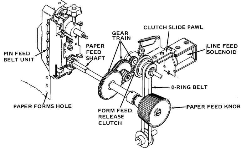
1.3.2. PAPER MOVEMENT (Figure 1-5)
Paper can be moved manually by rotating the platen knob or automatically by any of three paper movement commands: Line feed, vertical tab and form feed.
PIN FEED BELT UNIT
iLiNE FEED iSOLENOID
, ... ---"r-APER FEED KNOB
Figure 1-5. PAPER MOVEMENT MECHANISM
Power to drive the pin feed belt units controlling paper movement, is transmitted from the main motor through an O-ring belt to the form feed mechanism, where it is then transferred via the paper drive shaft to drive pulley for pin feed belt units. The form feed mechanism consists of a form feed or release clutch, a line feed solenoid with slide unit, and a gear train mechanically linking the main motor to the paper feed tractors.
To initiate a single line feed, the line feed solenoid is momentarily energized. Upon completion of the line feed command, a delay interval is generated, allowing the clutch pawl and clutch mechanism to return home before another line feed is allowed.
[image:13.611.73.458.257.495.2]/
Vertical forms movement is accomplished by applying a DC level to the paper feed solenoid. I n the standard 306 printer, this paper movement continues until it is either terminated by the rec-eption of a delete code (octal 177) or an INPUT PRIME signal at the interface connector, or a paper time-out condition. However, if the optional Vertical Format Unit (VFU) is used, the paper movement is terminated when a hole is detected in the appropriate channel of the vertical format paper tape.
As paper moves in the printer, each line advance causes a line count switch located in the form feed mechanism to open and close. -rhe two wires from this switch go to the interface connector via the logic card. As a result, a line count level from the input device is switched on and off by the printer for each line advance. If the 306 contains no optional VFU, the user's software can control vertical formatting by counting these line count pulses and terminating the paper movement operation when appropriate.
When the printer runs out of paper, a sensing switch activates a two-second audible tone in a speaker (option) located at the rear. The printer also stops printing and lights the PAPE R EMPTY light on the control panel.
1.3.3 SPECIAL FUNCTIONS
In addition to the printable characters and the carriage return, line feed, form feed, and verticall tab codes previously described, the printer also recognizes the following special control codes.
DE)lete (Octal 177) - Primes the printer electronics and clears the buffer.
Bell (Octal 007) - With Bell option only - Generates a two-second audible tone in the speaker
at the front of the printer.
Select (Octal 021) - Allows printer to receive data, same as activating SE LECT switch.
De-Select (Octal 023) -Inhibits printer from receiving data, same as deactivating SE LECT switch.
Elongated Boldface Characters (Octal 016) -Prints elongated characters on a line-by-line basis
(character-by-character controlled by bit 8, optional).
1.4
SPECIFICATIONS SUMMARYData Format
Input Code Data Rate Buffer I nput Gating
Data Input
7-bit parallel interface 8 bits (optional) 64-character ASCII
Up to 75,000 characters/second One-line character buffer
Rev. H
Printing
Printing Method Dot Matrix
Elongated Characters
Character Density Print Format Print Rate
Number of Copies
Character Sets
Paper Advance
Slew Rate Vertical Format
Vertical Format Control Paper Entry
Paper Ti meout Paper Feed Auto Line Feed
Impact, character-by-character 5 x 7 (std.), 9 x 7 (opt.) By line, via octal 016
By character, via bit 8 (opt.) 10 characters/inch (horizontal) 80-characters/line (max.) 120 characters per second
Prints original and up to four carbon copies.
Standard 64-character ASCII, lower case prints as upper case. Optional sets up to 128 characters, available.
4
inches/second6 lines/inch
2-Channel paper tape (opti'on) Bottom and Rear Paper Feed 'IO-second Paper Runaway Inhibit
Sprocket Feed, adjustable to 9% inch (24cm) paper. Automatic line feed on carriage return
Disabled by option.
Control
s/
I nd icators SwitchesIndicators Manual Controls
Auto Motor Control (Opt.)
Audio Alarm (Opt.)
ON/OFF, SELECT, FORMS OVERRIDE TOP OF FORM (OPT.) MANUAL LF (OPT.) SINGLE!DOUBLE LF (OPT.)
ON/OFF, SELECT, PAPER OUT Forms, Thickness, Paper Aldvance Knob Drive motor automatically turns off and on as required by the incoming data. Momentarily sounds a buzzer in response
to a Bell code or paper Hmpty condition.
Physical/Environmental/Electrical
Height Depth Width Weight
T
em peratu reInput Voltage
12-% inches (32.4 cm) 18-% inches (47.6 cm) 23-% inches (59 cm) 66 pounds (30 kg.) 400
to 1000
F (40 to
37.5°
C) (Operating) -400to 1600
F (-400to 71°C) (Storage)
115 VAC
±
10%, 60 Hz (Std.)230 VAC
±
10%,50 Hz (Opt.)Other Options
Auto Carriage Return on Line Feed, Vertical Tab and Form Feed Bottom of Form
I nhibit Delete Code
Serial Communications Interface Popular Parallel Computer Interfaces
Ribbons
The printer uses a 1-inch nylon ribbon mounted on 3-inch diameter spools. The following four colors are available:
Black - Part No. 63002293-5001 Red - Part No. 63002293-5002 Green- Part No. 63002293-5003 Blue - Part No. 63002293-5004
Centronics nylon ribbons are designed specifically for use in Centronics matrix printers. The fabric design and proprietary ink formulation ensures optimum print quality, as well as long print head and ribbon life.
Note: Centronics reserves the right to void the warranty with regard to any parts damaged through the use of non-qualified ribbons.
Paper
The printer used continuous form paper with standard feed holes on each edge. Paper widths from 4 to 9% inches (10.2 cm - 24.1 cm) can be accommodated by the printer. Using multiple-part form, one original and up to 4 copies can be printed, all very legible. Paper weight specifications are as follows:
Single-Part Forms: Multiple-Part Forms:
Carbon Paper:
1.5 PHYSICAL DESCRIPTION
15t0121b.
Original - 12 to 15 lb.
Copies - 9 to 12 lb., last copy 15 lb. (Maximum of five parts)
7% lb. with medium hardness
The printer is approximately 12-%"(32.4 cm) high by 18-%"(47.6 cm) deep by 23y;'(59 cm) wide, and weighs approximately 66 pounds (30 kg.). The complete printer is assembled on a base made of cast
alum-inum. Enclosin~ the printer are three removable plastic covers: the main cover, top cover and VFU covet.
The top cover can be opened to give access to the print head by tilting the cover back and lifting it
complete-ly off the printer. The VFU cover can also be tilted back or removed for access to the optional Vertical
Format Unit, if it is used.
Figures 1-6 to 1-9 are different photographic views of the printer taken with the covers removed. All
major assemblies are identified, in addition to
a
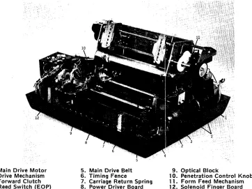
few other important components, the locations of which1. Print Head Assembly 5. Damper Piston 10. Pin Feed Mechanisms 2. Video Ampl. and Cable Ass'y 6. Operator Panel 11. Paper Feed Shaft 3. Carriage
4. Ribbon Cable
1. Main Drive Motor 2. Drive Mechanism 3. Forward Clutch 4. Reed Switch (EOP)
7. Damper Cylinder 12. Platen 8. Left Ribbon Feed 13. Platen Knob 9. Vertical Format Unit Option 14. Right Ribbon Feed
Figure 1-6. LEFT FRONT VIEW OF 306
5. Main Drive Belt G. Timing Fence
7. Carriage Return Spring 8. Power Driver Board
9. Optical Block
10. Penetration Control Knob 11. Form Feed Mechanism 12. Solenoid Finger Board
Figure 1-7. RIGHT FRONT VIEW OF 306
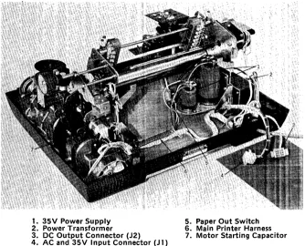
[image:17.611.122.487.56.354.2] [image:17.611.117.479.407.678.2]1. Logic/Power Supply Board 2. Logic/P.5. Fuses
3. AC and 35 V I nput Connector (J 1 ) 4. DC Output Connector (J2)
7. AC Power Input 8. Input Cable (W2) 9. Motor Control Option 10. Line Feed Solenoid 5. Input Connector 11. Line Count Switch 6. In-Line Fuse
Figure '-8. REAR VIEW OF 306
1. 35V Power Supply 5. Paper Out Switch 2. Power Transformer 6. Main Printer Harness 3. DC Output Connector (J2)
[image:18.611.148.483.73.382.2] [image:18.611.153.487.429.699.2]SECTIONS 2 AND 3
INSTALLATION AND OPERATION
A separate Series 300 Operators Manual contains most of the installation, set-up and operating procedures for the Model 306 printer. Reference should be made to this Operators Manual during normal printer installation and operation.
I ncluded on the following pages is additional information not contained in the Operators Manual.
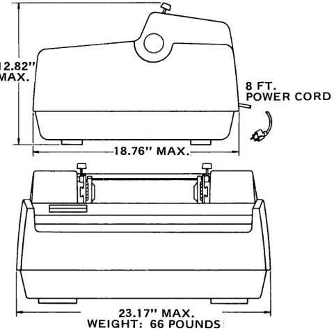
~~.1 SITE PREPARATION (Figure 2-1)
A line drawing of the printer dimensions is shown in Figure 2-1.
1
12.82"MAIt_---rl
I
23.17" MAX.
[image:20.611.230.470.237.475.2]WEIGHT: 66 POUNDS'
Figure 2-1. PRINTER DIMENSIONS
Environmental and electrical requirements at the installation site are as follows:
T em peratu re :
Humidity (%RH):
Electrical:
400 to 1000F (40 to 37.50 ) (operating)
-400 to 1600 F (-400 to 710C) (storage)
5% to 90% (no condensation) - operating 0% to 95% - storage
115 VAC
±
10%,60 Hz2.2 SHIPPING CRATE
The printer is shipped in a crate approximately 22 inches (55 em) high, 27 inches (68 cm) deep and
28 inches (71 cm) wide. The crate is made of weatherized, triple-walled cardboard. When properly strap-ped, the packing crate and printer is capable of fork lift operation with a seven-hig.h stacking capability.
Shipped with the printer are the following items:
A. Special Interface and Cable - If a special interface is used, the interface card is lincluded with
the printer. For certain interfaces such as the RS232, a special cable is also shipped. Cabling
requirements for the standard parallel interface are defined in Appendix
B.
B.
VFU Tape - If optional Vertical Format Unit is installed, a standard vertical format paper tapeproviding six line feeds one inch for each vertical tab and
66
lines (11 inches) for each formfeed code is provided. Refer to the Operators Manual for dupl icating the existing tape, or if a different format is desired, generating a new tape.
C. Documentation - All documentation describing that particular printer is included in a plastic
bag under the printer. This documentation includes a technical manual for the printer and any optional interface, and a notice of all approved changes incorporated in the printer, but not documentedin the manual. Please keep this ,documentation with the printer at all times so that accurate information will be available for troubleshooting purposes.
D. Pin Feed Knobs - These knobs are contained in a sma!1 plastic bag stapled to the guide bar for
the pin feed unit.
E. Print Sample - A sample printout from that particular printer is included in the upper paper pan.
F. Unpacking/Repacking and Set-Up Instruction Sheet.
SECTION 4
THEORY OF OPERATION
4.1 INTRODUCTION
This section on the theory of operation contains a detailed description of each major function per-formed by the electronics in the Model 300/500 Series printers. Figure 4-1 shows a basic functional dia-gram of the printer electronics.
Throughout this section, reference is made to the schematic diagrams contained in Section 7. The section is organized as follows:
4.2 BASIC TIMING
Paragraph: 4.2 Basic Timing
4.3 Initializing the Printer (Prime, Select)
4.4 Data Input (Data, Strobe, Busy, Acknowledge)
4.5 Data Storage
4.6 Character Printing
4.7 Paper Movement (Line Feed, Vertical Tab, Form Feed)
4.8 Special Functions (Bell, Paper Empty, Delete,
Motor Control)
4.9 Power Supplies
4.10 LSI Chips Inputs/Outputs
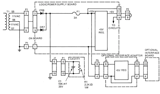
Timing for the printer electronics is provided by signal OSC, which is generated by Large Scale
Integrated (LSI) circuit ME14. The OSC signal frequency (125 KHz
±
125 Hz) is determined by acrystal controlled oscillator (Y1, ME6, ME15).
The oscillator crystal (Y1) establishes a reference frequency of 4 MHz, which is divided by : 16-counter ME 15 to provide a 250 - KHz signal at pin 26 of the 2010 LSI element (ME 14). Element ME 14
divides this signal by two, generating the OSC output signal of 125 KHz
±
125 Hz.The OSC signal is used by LSI elements ME13, ME14 and ME28 for internal timing. It is also double inverted by ME37-2 and ME34-12 to generate signal OSCXT. Signal OSCXT is routed to printer interface connector for use by an optional interface card.
4.3 INITIALIZING THE PRINTER
,
I
LOGIC/POWER SUPPLYI
PARALLELDATA INPUT
I
DATAl-DATA 8BOARD
I
r---..., PRINT WIRE
..
CONTROL,.>
~---rv'TB1-TB8 )
.... ~----r--v'
:>
INTERFACE CONNECTOR
\/
I DATA STROBE I
I
I
ACKNLG,BUSY
r
I
BUZZER (OPTIONAL)
VFU TAPE READER (OPTIONAL) OPERATOR PANEL
-DECODERS.
,
--VTH,FFH CONTROLS _ AND INDICATORS
-CLKTBl
RAM
UP ADDRESS
COUNTERS AO-A7
jCLKTB2
I
CONTROL TIMING
BUFFER (RAM's)
PAPER MOVEMENT
PMSOL
CHARACTER GENERATORS
(ROM's)
022 PRINT DCWl-5, DCW01-Q4 FWD CLUTCH
CONTROL
STROBE
I
STROBEI
TIMER
r - - - - l
VIDEO,
I
I
VIDEO ~ *JUMPERI
~~~ECT ~ ~I
I
CIP
*C:ONNECTEO FOR SINnl F
-I
iii-I
I
I I
I
VIDEOI ____________ ~C_H_A_N_N_E __ LOPE~ION ______ ~I
VIDEO AMPL
I
AMPLI
10USED IN
0'
I MODEL 306C
I
I
ONLYI
I
L _ _ _ - - I
Figure 4-1.
I
LIMITSWITCHES
SERIES 300/500 BLOCK DiAGRAM
-DRIVER CIRCUITS
...
TO PRINT HEAD SOLENOIDS
4.3.1 PRIME
The PRIME signal, generated by LSI ME14-37, is initiated by any of the following conditions: A. Power Turn - on - .When the ·printer is powered - up, capacitor C7 is initially discharged causing a
100 to 500 - millisecond PWR PRIME signal at ME14-32. This generates a high PRIME signal at IVIE'14-37. As C7 charges to +5 Vdc, PRW PRIME goes high, terminating the power prime operation.
B.
Printer Selection - If the Delete Inhibit option (DELlNH) is not used (i.e.,jumper X1-3 to 14 is con-nected), thena
low SLCT input to ME14-40 and a high DELINH to ME14-39 generates a 100 to 400 - microsecond P RIM E pu Ise from ME 14-37.C. End of a Printed Line - At the end of a line of print, CIPX from ME14-30 goes high, turning off the forward clutch and generating a 100 to 400 - microsecond PRIME pulse at LSI ME14-37.
D. Delete Code - Receiving a delete code (octal 177) * on input data lines DS
1
through DS7 generatesa low DCPRM output from LSI ME13-S. Signal DCPRM in turn initiates a 100 to 400-microsecond PRIME pulse from LSI ME14-37. Recognition of delete code can be inhibited with jumpers X4-15 to 1 and X4-9 to 7 (Delete Code Inhibit option).
E. Input Prime - Reception of
a
low INPUT PR I ME signal via the interface connector generates a high IP signal into LSI ME13-36. This produces a DCPRM output from LSI ME13-S (same asthe delete code), which in turn initiates a 100 to 400-microsecond PRIME pulse from LSI ME14-37. In all the above cases, the high PRIME signal from LSI ME13-36 resets the printer logic and causes ME32-3 to generate a parallel enable signal for PE input of up-counters ME9 and ME10. This presets the outputs of the up-counters to conditions present on the jam inputs (pins 3, 4, 12 and 13 of M E9 and ME 1 OL These inputs can be programmed for an SO or 132 column printer via a jumper option (X2-4 to 13 for an SO-column printer).
4.3.2 SE LECT /DESE LECT
\Nhen the printer is selected, it is conditioned to receive and process data for printout. When deselected, only the Select (octal 021) or Delete (octal 177) code is recognized by the printer.
4.3.2.1
SelectThe printer is selected by either of the following conditions:
A. Operation of the SE LECT switch when the printer is deselected.
B. Reception of an octal 021 code.
When the SELECT switch is depressed, a high SELSW signal appears at LSI input ME13-31. Approx-imately 2-S milliseconds after SELSW goes low, a latch in LSI ME13 is set, causing the SLCT' output (LSI ME 13-40) to go high.
The LSI select latch is also set when an octal 021 code, appearing on LSI ME13 inputs DS1-DS7, is added with ungated data strobe pulse DST A.
4.3.2.2 [)eselect
The printer is deselected (i.e.,the internal select latch is reset in 2009 chip ME 13) either by again pressing the SE LECT switch or by an octal 023 appearing on data lines DS1-DS7 with a DSTA pulse. Alternately pressing the SE LECT switch alternately selects and deselects the printer. Note that when power is turned on, PWRPRM resets the internal select latch so that the printer initially appears in a deselect state.
A high SCL T' signal at ME 13-40 indicates that the printer is selected. This signal, inverted by ME16-12 (SLCT), lights the SELECT lamp on the operator panel. SLCT is inverted by ME21-6, gen-erating a SLCT signal to the interface connector.
If DE LI N H jumper (X 1-2 to 14) is connected, then selecting the printer will also cause a prime condition. If jumper X1-3 to 14 is connected, then selecting will not cause a prime condition.
4.4 [)ATA INPUT
Inputs to the printer consists of seven standard parallel data lines (DATA1 - DATA7), an active low DATA STROBE input, and an active low input prime (INPUT PRIME) line. The first seven data lines receive the 7 bit USASCII code shown in Figure 4-2.
tt
6 b5Bj
ts bbbb~ 4 3 2 1
Row
0 a a 0 a 0 a 0 1 1 a 0 1 a 2
-0 a 1 1 3 0 1 0 a 4 a 1 a 1 5 0 1 1 0 6 0 1 1 1 7 1 0 0 a 8 1 a 0 1 9 1 0 1 a 10 1 0 1 1 11 1 1 a a 12 1 1 0 1 13 1 1 1 a 14 1 1 1 1 15
000 00 1
a 1
NUL OLE SOH DCl STX DC2
I---ETX DC3 EOT DC4 ENO NAK ACK SYN BEL ETB BS CAN HT EM LF SUB VT ESC FF FS CR GS
f
-SO RS SI US
....-CONTROL CODES
0
10 all 10
0 101 110 111
2 3 L~ 5 6 7 SP a @ P , p ! 1 A 0 a q " 2 B R b r
# 3 C S c 5 $ 4· 0 T d t
% 5 E U e u
& 6 F V f v
7 G W 9 w
( 8 H X h x
) 9 I Y i y
* J Z j z
.
-+ ; I( [ k {
< L \ I I
- M ] m }
---> 1\:
"
n ~/ ? 0 - 0 DEL
\ '~
-v-STANDAIW OPTIONAL
NOTE: Underscore (octal 137) is replaced by a backarrow in the standard 9x7 matrix.
Figure 4-2. USASCII CODE
The optional eighth bit is used as a control bit to specify an elongated character or select an additional character set. The data strobe is used to synchronize input data with the printer electronics. The input prime line (INPUT PRIME) is used to prime the printer electronics.
The eight data inputs have a unity loading factor and are terminated by a 1 K pull-Up resistor to +5 volts. The DATA STROBE and INPUT PRIME inputs are terminated by a 470 ohm resistor to +5
volts. Note that with no input on DATA
8
line terminating resistor R 15 holds the input at +5V andmakes bit
8
appear as a ON E on the logic card.In response to received data, the printer generates an ACKN LG pulse to acknowledge reception of a character. If the received character caused the printer to perform some function such as paper move-ment, character printing, etc. , the printer responds with a BUSY signal.
4.4.1 DATA INPUT TIMINIG
I n general, the data transfer sequence consists fo the input device placing the appropriate code on the data lines to the printer and then generating a data strobe pulse. The printer, after a slight delay, responds with an acknowledge pulse. Or if the received data caused a busy condition, the printer first activates the busy line for the duration of the busy condition and then responds with an acknowledge pulse.
Figure 4-3 provides the timing involved during a normal data input condition (not busy) or a busy condition in Centronics printers that use the 300/500 Logic/Power Supply Board (63060416).
4.4.1.1 Normal Data Input - No Busy
__ As...§hown in Figure 4-3, each data line must be stable at least 1.0 microsecond before and after DATA STROBE, and the DATA STROBE pulse must be at least 1.0 microsecond long. I n response to the received data, some 2.5 to 10 microseconds after the trailing edge of DATA STROBE, the printer generates a 2.5 to 5.0 microsecond ACKNOWLEDGE pulse, indicating that it is ready to receive additional data. As a standard feature, the printer will not recognize a data strobe pulse during the acknowledge delay interval. As an option, non-gated strobe is available.
4.4.1.2 Data I nput Causing Busy
As shown in Figure 4-3, the printer responds to any of the functions listed in the table under Busy Duration by generating a BUSY signal from 0 to 1.5 microseconds after the trailing edge of DATA STROBE. As shown, the duration of BUSY depends on the specific function being performed.
From 0 to 10 microseconds after BUSY is terminated, the printer generates a 0.5 to 5.0-microsecond ACKNOWLEDGE pulse to indicate that the specified function is completed.
4.4.2 BUSY
A busy indication is developed by LSI chip ME 13 pin 11. This BUSY output, normally high when the printer is not busy, goes low when any of the following conditions occur:
-A. CSBSY goes low - This occurs during anyone of the following conditions:
1. During a bottom of form detection (VTH and FFH are high).
2. When a paper motion command is received while the motor control circuit is timed out.
CSBSY goes low for approximately 300 milliseconds.
3. When signal DMC goes high, indicating that a full line of data has been stored.
B. PR I ME goes h igh- This occurs during a prime operation as described in Section 4.3.1.
C. LFF (internal to ME13) goes high - This occurs either when a form feed code (octal 014) is
received or the optional TOP OF FORM switch on the operator panel is pressed. (Note: If thEl DSC option is used, the received FF code will first cause the line to be printed before activating LF F). LF F is normally reset by the trail ing edge of D L Y LF.
D. LLF (internal to ME 13) goes high - This occurs when a line feed code (octal 012) is received
PARALLEL DATA
~~;tJ.YJ.1/b1J1~
_--.J1.0'us
L
~1.0 us ~ DATA STROBIl/MIN)r
-I(MIN)~
L~~---.l
~ 1.0 us (MIN)I
I
500 us (MAX)ACKNOWLEDGE ______________________________ ~I ~
\ . - - A C K DE LA Y - - 3 1 = A C K - - - \
I
(For Normal Data)-...j
ACK DELAY BUSYW'ffffa
I
(For Busy Condition)BUSY DELAY4 r--BUSY---l
NORMAL DATA INPUT TIMING
301 306 306C 500 501 588
ACK DELAY 2.5-10 usee 2.5-10 usee 2.5-10.0 usee 2.5-10 usee 2.5-10 usee 2.5-10.0 usee
ACK 2.5-5.0 usee 2.5-5.0 usee 2.5-5.0 usee 2.5-5.0 usee 2.5-5.0 usee 2.5-5.0 usee
BUSY CONDITION TIMING
BUSY DELAY 0-1.5 usee 0-1.5 usee 0-1.5 usee 0-1.5 usee 0-1.5 usee 0-1'.5 usee
ACK DELAY 0-10.0 usee 0-10.0 usee 0-10.0 usee 0-10.0 usee 0-10.0 usee 0-10.0 usee
ACK 2.5-5.0 usee 2.5-5.0 usee 2.5-5.0 usee 2.5-5.0 usee 2.5-5.0 usee 2.5-5.0 usee
BUSY DURATION:
Line Feed 50 msee 76 msee 76 msee 76 msee 50 msee 76 msee
(single LF) (single LF) (single LF) (single LF)
100 msee 152 msee 152 msee 100 msee
(double LF) (double LF) (double LF) (double LF)
Vertical Tab (I-inch) 165-175 msee 310-320 msee 310 - 320 msee 310-320 msee 165-175 msee 310-320 msee
Form Feed (II-inches) 1.5-2.0 see 2.8 - 3.3 sec 2.8 - 3.3 sec 2.8 - 3.3 see 1.5-2.0 sec 2.8 - 3.3 sec
Delete 100-400 usee 100-400 usee 100-400 usee 100-400 usee 100-400 usee 100-400 usee
Bell 0 0 0 0 0 0
Select 100-400 usee 100-400 usee 100-400 usee 100-400 usee 100-400 usee 100-400 usee
Deselect Until printer Until printer Until printer Until printer Until printer Until printer
is selected is selected is selected is selected is selected is selected
Print Command 6 msec/char 8.4 msec/char 10 msec/char (10 epi)* 8.4 msec/char 6 msec/ehar 11.3 msec/char
plus 50 msee plus 76 msec 8.4 msec/char (12 cpi) plus 76 msec plus 50 msec plus 76 msec
LF LF 6.6 msec/char (15 cpi) LF LF LF
6.0 msec/char (16.5 epi) plus 76 msee (LF)
(Return time-no busy) (270 msec (270 msee (270 msec (400 msec (400 msec (400 msec
max) max) max) max) max) max)
kCpi = Characters per inch
Figure 4-3. DATA INPUT TIMING
E. L TF (internal to ME 13) goes high - (Similar to the LF F signal) - L TF goes high when a vertical tab code (octal 013) is received and is reset by the trailing edge of D L Y LF.
F. DCPRM goes low - This occurs under any of the following conditions:
1. Reception of a delete code (octal 177).
2. Reception of an INPUT PR I ME signal at the interface connector.
3. During a power prime (PWRPRM) condition.
G. REMCR (internal to ME13) goes high - This occurs when a control character is clocked into memory,
indicating the start of a character printing operation. I n the standard printer configuration, only the carriage return control code (octal 015) is stored into memory. However, if the DSC option is used (jumper X 1-4 to 13), then a LF, VT, F F or CR code (octal 012, 013, 014 and 015, respectively) can be loaded into memory.
H. PMSO L goes low - This occurs while the paper movement solenoid is activated.
I. FAU L T goes high - This occurs under any of the following conditions:
1. The printer is de-selected (SC L T' is low).
2. The printer is out of paper (PE is low).
3. During a paper time-out condition.
4. During a I ight detect (LD) error condition. Signal LD goes low when there is not a video signal
detected as the print head travels across the page.
J. DLYLF goes high - This line feed delay occurs following a paper movement operation. The DLYLF
signal is either approximately 40 or 60 milliseconds, depending on the printer configuration.
As shown in the timing diagram in Figure 4-3, BUSY can occur up to 1.5 microseconds after the trailing edge of DATA STROBE. The worst case (1.5 usec) condition arises when CSBSY goes active.
This occurs because of the accumulated de~s in 10adi..Q.9. the last character in a line of data into memory,
detecting a maximum count indication at CO output (CO low) of upcounter ME10, generating CSBSY' on LSI chip ME14 and finally generating BUSY on LSI chip ME13.
4.4.3 DECODERS
The buffered data inputs along with a data strobe input are applied to two decoder networks. One decoder network (First Decoder) is comprised of elements ME17 through ME20, ME26 and ME27. The other decoder network (Second Decoder) is contained in LSI chip ME13.
4.4.3.1
First Decoder
The First Decoder (ME 17 through ME20, ME26 and ME27) detects the following:
A. Delete code (octal 177) for the delete code inhibit option.
B. Character density select code (octal 022). This code is gated and is only used in the Model 306C
4.4.3.1.1 Delete Code Inhibit (option)
If the printer is configured with delete code inhibit (X4-16 to 1 and X4-10 to 7), detection of an octal code 177 on the data input lines causes a low output at ME2Ei-3 (177). Signal 177 causes the following:
A. Inhibits CLKTB 1 pulses via ME32-11.
B. Drives DS6 and DS7 high, converting octal 177 to octal 037. The Second Decoder (ME13)
acknow-ledges (ACK) the code but does not initiate any function.
4.4.3.1.2 Character Density Selection (Model 306C Only)
When jumper platform X4 pins 11 to 6 are connected and a hardwire connection is made between E 1 and E2, this enables the Model 306C to select character density.
CAUTION
E1 IS CONNECTED TO E2 ONLY FOR THE MODEL 306C, OTHER\NISE DAMAGE WILL RESULT.
Jumper X2-2 to 15 is also connected when the Model 306C printer is configured with an 80/132, 96/132, 80/120 or 96/120 dual-timing fence. This enables the Video Select Circuit to change the strobe delay time in the universal timing chip (ME28) from 660 to 370-microseconds when switching from 80 or 96 characters per full line to 132 or 120 characters per full line, respectively. See Appendix A for all timing programmed into ME28.
The detection of an octal 022 code sets latch output (ME20-11) high. This output is reset by PR I ME. When ME20-11 goes high, it causes the following:
A. Drives ME39-4 low. This output appears at jumper pin X2-2. \Nhen X2-2 to 15 is connected as
des-cirbed in the previous paragraph, the strobe delay time will change from 660 microseconds to 370 microseconds.
B. Enables ME43-11 output to track CHAN2 video pulses. If the VI DEO CONT signal is high, set by a NORMAL/CONDENSED switch operation, reception of octal 022 code will cause ME43-11 output to track the video signal opposite to that selected by the switch and, depending on the printer configuration, changes the strobe delay timing.
4.4.3.1.3 Character Elongation (Octal 034) - Special Option
When the printer is configured to recognize octal code 034 instead of 016 to elongate characters by line (X5-6 to 11 and X5-12 to 4), detection of octal code 034 and associated data strobe (DSTA) sets a latch (ME27), driving UCC SET low to ME14-21. The latch is reset by PRIME.
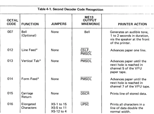
4.4.:3.2 Second Decoder
The Second Decoder is located in LSI chip ME 13. The octal codes recognized by the Second Decoder are listed in Table 4-1. The table provides the following information:
A. Code function
B.
Jumper (s) necessary to enable the code function. [image:30.611.73.572.354.724.2]C. Signal mnemonic of the resultant output. D. Resulting printer action.
Table 4-1. Second Decoder Code Recognition
AL OCT COD E
007
012
01~ l
014
01&
016
FUNCTION Bell
(Optional)
Line Feed*
Vertical Tab*
Form Feed*
Carriage Return Elongated
ME13 OUTPUT
JUMPERS MNEMONIC
None Bell
-None CSLF,
PMSOL
None PMSOL
None PMSOL
-None DSCR
-X5-1 to 15 UPSC
-PRINTER ACTI ON Generates an audible to ne,
on, rant 1 to 2 seconds in durati via the speaker at the f of the printer.
Advances paper one lin
e.
Advances paper until t he next hole is reached in channel 5 of the V F U paper tape.
Advances paper until t he next hole is reached in channel 7 of the V F U t ape. Prints line of stored da tao
ME13
OCTAL OUTPUT
CODE FUNCTION JUMPERS MNEMONIC PRINTER ACTION
021 Select ** None SLCT~ Can receive data. Jumper
X1-3 to 14 inhibits a prime operation during select.
023 Deselect ** None SLCT' Will not recognize any input
data except a Select (021) or Delete (177) code.
177 Delete ** None DCPRM Printer is primed.
Note 1
If printer has the Delete Inhibit option, Delete code (177) will be acknowledged but not acted on.
Note 2
In Model 306C only, the character density returns to that set by the NORMAL/ CONDENSED switch.
*If the DSC option is used (jumper X1-4 to 13), LF, VT, and FF also cause the stored line of data to be printed. If the printer does not have DSC option and the code is received in the middle of a line of data, paper is advanced immediately without loss of data.
* *This code will also be recognized during a busy condition.
-I n addition to functions listed in the Table 4-1, the Second Decoder monitors input data for the
first printable character (i.~., a high on bit 6 or 7). Detection of the first printable character enables the
printer to respond by printing the line of characters under either of the following conditions:
A. Recongnition of a carriage return code.
B.
If the DSC otpion is used, recognition of a Line Feed, Vertical Tab or Form Feed code.4.5 DATA STORAGE
The printer storage buffer consists of two Random Access Memory (RAM) elements. Up-counters are used to address the RAM elements and determine when thE!re is a full line of characters in storage. Depending on a jumper option, 80 characters (X2-4 to 13) or '132 characters (X2-4 to 13 not connected) will be detected as a full line of data.
4.5.1 TIMING OF UP COUNTERS AND RAM ELEMENTS
A.
B.
C.
D.
Rev. I
The actual timing involved depends on which one of the ifollowing printer operations is taking placf~:
A prime condition.
Data reception.
Reception of a carriage return code (octal 015) prior to a full line of data (depending on mode of operation, the 80th or 132nd character in a line).
Printing a line of characters.
4.5.'1.1 Priming the Up Counters
As shown in Figure 4-4, a prime condition will cause a positive pulse to appear at the preset enable (PE) input of up-counters MEg and ME 1 O. The leading edge of this signal preset' the counters to the load conditions present on the jam inputs (pins 3, 4, 12 and 13) of each counter. These conditions are reflected on the RAM address bus lines AO through A7. There are two load conditions:
A. For an aO-column printer, where jumper X2-4 to 13 is connected to preset the counter to decimal
count 175 (octal 257).
B.
For a 132-column printer, where jumper X2-4 to 13 is not connected and the counter is preset todecimal 123 (octal 173).
2nd
CHARACTER
15t 3rd
CHARACTER CHARACTER
80th
CHARACTER
DAT A I NPUT _ _ _ _ --"'-ILI.U.:L----'-~'"'__...KR~.&.__It~< _"",WllhI~u.-
__
(DATA 1 - DATA 7) . 7
DSTA _ _
----'nL--_~n~_~f_n--(ME13-18) CLKTB1 (ME32-11) CLKTB1 (ME42-10) CLKINPUT (MEg, ME10 PIN 15)
PRIME ENABLE (ME7, ME10 PIN 1)
AO
A1
A2
RAM A3
ADDRESS BUS
A4
A5
A6
DATA WRITTEN INTO MEMORY
---.+
U
U
,
I'
r-'f-1J+
u
I I I I I I I
I I I I I I I I
,_---In.
h
Lt-li---' _ _ _ _ _
~~:
:uPDATE FArADDRELr~S ~~:
PRESET e820
U
INITIATESCOUNTERS m5ec DUMMY
~1~~deJ~~
t :
II : I'CHARACTERPRINTE,R)
n
I I I INDICATIONI I (DMC)
I
(r---~I---1 st I 2nd I 3rd I
ADDRESS,I .... ADDRESS ADDRESS_! 80th I
,
,
"r'---~'WM(175 10 ) (17610) 1(177 10)
I
~~~~'_----II""'""-C~I
~f--,
WJ1
Iir-I
Wlt1
r
I
I
WlA
I•
f
I
fr---Wi1
II
~
II
4.5.1.2 Normal Data Input
Each time a printable character or CR code (octal 015) is received during normal data input to the printer, LSI element ME13 causes the generation of CLKTB1 and CLKTB1, slightly delayed from data strobe.
Assume that a full line of data is being received and the board is configured for an 80-column/line printer (See Figure 4-4). The data strobe (DSTA) received with the first character in a line causes ME32-11 and ME42-10 to generate CLKTB1 and CLKTB1. During CLKTB1 the Random Access Memory (RAM) elements write the data for the first character into the preset RAM address (decimal 175 for and 80-column printer).
The trailing edge of CLKTB 1 causes a clock signal (approximately 820 nanoseconds) to appear at CLK input of MEg and ME10 pin 15. The trailing edge of this clock pulse increments MEg to the next count, providing the next RAM address. The second character received by the printer is then written into this address. Approximately 820 nanoseconds later, the address for the third character appears on the RAM address bus. This sequence continues until the 80th charalcter is received and written into RAM address decimal 254. On the trailing edge of this CLKTB 1, the RAM address is updated to decimal 255. At this time, the carry out (CO) output (ME10 pin 7) goes low, indicating maximum count of ME10. The CO output is gated and inverted via ME32-4, providing a dummy character indication (DMC) to the 2010 LSI input ME14-34. This causes the printer to go busy and activates the forward clutch.
4.5.1.3 Following a Carriage Return
Following the reception of a carriage return code (octal 015), ~;ignal DSCR goes low, providing a
dummy character recognition (DMC) to LSI input ME 14-34. This causes the printer to go busy and activates the forward clutch.
4.5.1.4 During Character Printing
After a line of data has been stored and a start print condition is detected by LSI ME 14, ME 14-30 generates a CI PX signal. This activates the forward clutch and causes the print head assembly to move along the timing fence.
The CI PX signal remains low during the print cycle, providing a high at input ME31-9 and two signals (CIPM and CIP) for the motor control logic.
As the print head assembly moves along the timing fence, the first window in the fence causes the logic to switch from DCWO time to DCW1 time and ME14-36 to generate a CLKTB2 pulse (Refer to Figure 4-5). Signals CLKTB2, CIPX and high output of ME31-12 are ANDed to generate a preset enable signal to up-counters MEg and ME 1 0 via ME32-3. This presets the counters to the first RAM address. Thus, the first character written into memory is the first character printed.
On the trailing edge of the first CLKTB2 pulse, ME31 is clock1ed, driving ME31-12 low. This enables ME27-11 to track each subsequent CLKTB2 pulse, updating the memory on the trailing edge ()f each DCWO interval.
CIPX (ME14-30)
CLKTB 2 (ME 14-36)
START PRINT CYCLE
,
CHARACTER DATA
_~n
n
n~_
!4--(DCWO· ~I+-(DCWO·...,..I
COUNTERS : I
*
PRESET ~I DCWS} I DCWS} IPR ESET ENAB LE , I
(ME32-3) - - - ' , UPDATE RAM ADDRESS
CLOCKINPUT---I---~U
11
( M E 9, 1 0-1 5) .
I 1st 2nd
RAM ADDRESS BUS
I ADDRESS I ADDRESS I
1/
~I/
""""'r--'--~I'I'I'I'I'I'I'I'I'I'I'I'I'~
(
17S 10)I (
176 10)I
AO.
VI'I'I'I'I'I'I'I'I'I'I'I'I'I'
I
J
Al~
IA 2 _ i W M
A3.Wff$a
I I
A4~
I
I
A5W~
A6 _ _ _
I
,
A7
wnffffM
I
I.
4.6 CHARACTER PRINTING
Character printing is initiated when LSI chip ME14 detects a high on pin 14 (DMC) indicating a decoded Carriage Return or buffer full condition (up-counter ME 1 0 reached maximum count). The
DMC input to ME14 is recognized during any time except when ME14 generates CIPX or PRIME. When DMC is recognized, the logic activates an electromechanical clutch that causes the print head to move from left to right across the page.
As the print head carriage moves across the page, the timing fence and optic pick-up assembly generates timing pulses to the video amplifier. These timing signals are used by the logic to register the five
full-step columns of dots in the printed character.
Depending on whether a 5 x 7 or 9 x 7 character matrix is used for character generation, the logic uses either one or tvyo Read-Only Memory (ROM) elements for each character set. One ROM defines the dot pattern for the five full-step columns, the other defines the dot pattern for the four half-step columns in a 9 x 7 matrix.
This section describes the character printing operation in the following sequence.
Paragraph 4.6.1 I nitiating Print Operation
4.6.2 Character Registration and Timing
4.6.3 Character Generator (ROM)
4.6.4 Print Head Operation
4.6.5 Power Driver Circuits
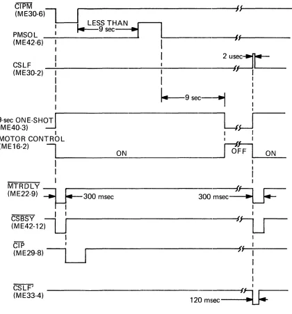
4.6.1 INITIATING PRINT OPERATION
As data is received by the printer, the count is increased incrementally in the up-counters until the maximum count is reached (full line of data). This drives ME10-7 (CO) low, Causing ME14-34 (DMC) to be driven high. This DMC input is also driven high when signal DSCR is driven low by the reception of a carriage return code (octal 015).
When LSI chip ME 14 recognizes a high DMC signal, it generates a low carriage in print signal (CIPX).
As shown in Figue 4-6, the CI PX signal is double inverted and routed to:
A. Inverter ME34, where CIPM is inverted by ME34-4 to generate CIP.
B. The Motor Control circuit, where CIPM resets a retriggerable 9-second one-shot. If a paper
move-ment command (CSLF or PMSOLD) or another print command (CIPM) has not been received for
nine seconds, a 300-millisecond Motor Delay (MTRDL Y) signal is generated.
The MTR D L Y signal causes a 300-millisecond busy condition while delaying the generation of CI P
via ME29-S. The delay is effective when the printer has the Motor Control feature. The Motor Control feature is discussed in paragraph 4.8.4.
MOTOR MTRDLY CAUSES CONTROL ... ----~ BUSY
CIRCUIT ~ FOR 300 msec
300msec
POWER DRIVER BOARD
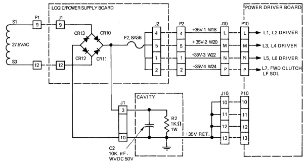
FWD CLUTCH
Pl0
Figure 4-6. FORWARD CLUTCH INTERCONNECTION DIAGRAM
W96 FWD CLUTCH
When signal CI P goes low, it activates the forward clutch via the Power Driver Board, causing the carr~age assembly to move from left to right.
A limit switch is located at the right (RTP switch) and left (EOP switch) end of print head travel. They are actuated by a magnet mounted on the underside of the carriage mechanism. Actuation of the RTP or EOP switch indicates that the carriage is at the extreme left or right position, respectively.
Signals i~TPSW and EOPSW generated by the switches are applied to LSI chip ME 14 to control the
forward clutch logic (CI PX) and to detect failure in the video signal from the timing fence (LD goes low).
When the EOP switch is actuated or a control code is detected by LSI chip ME 14 (=fB6 and TB7 signal high), CIPX goes high, turning off the forward clutch. This results in returning the print head to the left margin.
4.6.2 CHARACTER REGISTRATION AND TIMING
As the carriage assembly moves from left to right, the optic pick-up assembly on the video amplifier board generates the video signal for controlling the print timing. As the print head moves across the page, the optic pick-up assembly scans the alternate transparent-opaque bar pattern on the timing fence, gen-erati ng a video signal.
Depending on the timing fence and video amplifier used, single channel or dual channel (Model 306C Only), CHANNEL 1 or CHANNEL 1 and CHANNEL 2 signals will be generated and routed to the Logic/ Power Supply Board (Logic Board) via the Power Driver board (See Figure 4-7).
If the single-channel timing fence and video amplifier are used, signal CHANNEL 1 is routed through a jumper (X4-5 to 11) to the VIDEO input of LSI chip ME28 on the logic board. If the dual-channel timing fence and video amplifier are used, signals CHANNEL 1 and CHANNEL 2 are routed to the Video Select circuit (ME39 and ME43) on the logic board. The signal selected by the Video Select circuit is routed through a jumper (X4-6 to 11) and appears at the universal timing chip ME28 as signal VIDEO.
NOTE
The VI DEO signal causes ME28 to generate a STROBE signal, initiating the print timing shown in Figure 4-8. (Timing shown for Model 306 and 500. For timing related to Model 301, 501, 588 and 306C printers, see Appendix A).
If a 9 x 7 dot matrix is used, the leading edge of STROBE initiates a delay interval (internal to LSI chip ME28) between STROBE and Delayed Strobe (DL YSTB). The duration of the STROBE and D L YSTB pulses are the same. I n normal character printing, STROBE is used for full-step timing and DL YSTB for the half-step timing.
4.6.2.1 Video Amplifier
The single-channel (63060330-4001) or dual-channel (63060374-4002) video amplifier assembly is mounted on the carriage assembly. Each video amplifier channel Gonsists of a photo transistor in the optic pick-up assembly and a comparator circuit. The phototransistor converts the light monitored through the timing fence into an analog video signal. This signal causes the comparator to generate a pulsing output (VIDEO) that is routed to the logic board via the power driver board (See Figure 4-7). The duty cycle of VI DEO is set by the potentiometer connected to the other comparator input.
When the dual-channel video amplifier is used (Model 306C Only), the VI DEO 1 output reflects the top bar pattern on the timing fence, while VI DEO 2 reflects the lower bar pattern.
4.6.2.2 Video Select Circuit (Model 306C Only)
The Video Select Circuit is located on the logic board and consists of elements ME39 and ME43. This circuit selects either CHANNEL 1 or CHANNEL 2 signal as a VIDEO input to the universal timing chip ME28 and, depending to the timing fence used, can change the strobe delay time via the MODE input of ME28.
The Video Select circuit has four inputs:
A. Two control lines - VI DEO CONT and input from First Decoder (022).
1. VI DEO CONT - This input is low when the NORMAL/CONDENSED switch is set to
NORMAL position and goes high when the switch is set to the CONDENSED position.
2. I nput from First Decoder (022) - This is a gated input and goes high when a octal 022 is
monitored on the printer input data lines.
B. The video signal inputs - CHANNEL 1 and CHANNEL 2. These signals are generated by the
During a prime condition, PRIME resets the 022 input from the First Decoder, driving ME39-11 high. ""hen the NORMAL/CONDENSED switch is set to NORMAL position, VIDEO CONT is low and sets exclusive OR gate output ME39-11 low. This drives the MODE output (ME39-4) high and enables the VIDEO output (ME43-11) to track the CHANNEL 1 signal. If the switch is set to the CONDENSED position, the MODE output goes low and the VIDEO output tracks the CHANNEL 2 signal.
When an octal 022 code is detected, ME39-13 input is driven high. This input is OR'ed with the VI DEO CONT signal, causing the VI DEO output to track the signal opposite to the signal selected by the NORMAL/CONDENSED switch setting. The state of the MODE output is changed accordingly.
4.6.2.3
Strobe and Delay Strobe TimingThe universal timing chip (ME28) generates the STROBE and DL YSTB signals. The timing of these signals, along with a delay between STROBE and DL YSTB (internal to ME28), are determined by the conditions set by the X2 jumper platform configuration. See Appendix A, it provides all the timing set by the X2 jumper platform according to the printer model and timing fence used in the printer.
I n the Model 306C, the strobe delay time is selected by the Video Select Circuit via jumper X2-2 to 15 whenever the printer is configured with an 80/132, 96/132, 80/120 or 96/120 dual-timing fence. The strobe delay time is changed from 660 to 370 microseconds when the printer switches from 80 or 96 characters per full line to 132 or 120 characters per full line, respectively.
4.6.2.4
Matrix Column TimingThe LSI element ME14 has two strobe counters. They establish the timing involved to print each
column in the 5 x 7 or 9 x 7 do~ matrix of a character (See Figure 4-9). One strobe counter (full-step) is
clocked by the trailing edge of STROBE. The other counter (half-step) is clocked by the trailing edge of DL YSTB.
The full-step counter establishes times DCWO through DCW5. Time DCWO corresponds to the space between characters.
During time DCW1 through DCW5, ME14 generates signal DCW1 through DCW5. These signals correspond to the full step columns in the 5 x 7 or 9 x 7 dot matrix.
The half-step counter establ ishes times DCWO 1 through DCW04 and causes ME 14 to generate signals DCW01 through DCW04. These signals correspond to the half-step columns in a 9 x 7 matrix.
During elongated character printing, the UCC latch (internal to ME 14) allows alternate STROBE and DL YSTB pulses to clock the full-step and half-step counters, respectively. This results in all full and half-step DCW times being twice as long during elongated character printing than during normal
::0
CD
::::
--...
--...
"
--
./'0...---c.Q'
DCW1- = \
DCW1-c::
...,
DCW01-CD
c.o
~ (J'1
cO
x -...J DCW2- xDCW2-DCW02- -...J
0 Z 0 DCW3-
c.a
Z DCW3- '>c.n
0
("') :0 DCW03- :0
:E
s:
s:
DCW4--I ):> DCW4- ):>
-
r DCW04- rs:
DCW5-DCW5-Z
G>
Z
0
::tJ
s:
~
»
~
r
DCW1-DCW1-0
»
z
0 DCW 1 /DCWO 1-
DCW1-m
r
0 DCWO 1 /DCW2-
DCW2-Z
G> c.o (J'1
»
x DCW2/DCW02- xDCW2---! -...J ...
,
m m m
0 r DCW02/DCW3- r
DCW3-("') 0 0
Z Z
I G') G')
DCW3-»
):> DCW3/DCW03- ):>::tJ --I --I
»
m m("') 0 DCW03/DCW4- 0
DCW4--I
m
::tJ DCW4/DCW04-
DCW4-Cf)
DCW04/DCW5-