J. Phys.: Condens. Matter 22 (2010) 084018 (16pp) doi:10.1088/0953-8984/22/8/084018
Probing surface and interface structure
using optics
J F McGilp
School of Physics, Trinity College Dublin, Dublin 2, Republic of Ireland
E-mail:[email protected]
Received 30 April 2009, in final form 25 May 2009 Published 5 February 2010
Online atstacks.iop.org/JPhysCM/22/084018
Abstract
Optical techniques for probing surface and interface structure are introduced and recent developments in the field are discussed. These techniques offer significant advantages over conventional surface probes: all pressure ranges of gas–condensed matter interfaces are accessible and liquid–liquid, liquid–solid and solid–solid interfaces can be probed, due to the large penetration depth of the optical radiation. Sensitivity and discrimination from the bulk are the two challenges facing optical techniques in probing surface and interface structure. Where instrumental improvements have resulted in enhanced sensitivity, conventional optical
techniques can be used to characterize heterogeneous adsorbed layers on a substrate, often with sub-monolayer resolution. Nanoscale lateral resolution is possible using scanning near-field optics. A separate class of techniques, which includes reflection anisotropy spectroscopy, and nonlinear optical probes such as second-harmonic and sum-frequency generation, uses the difference in symmetry between the bulk and the surface or interface to suppress the bulk contribution. A perspective is presented of likely future developments in this rapidly expanding field.
(Some figures in this article are in colour only in the electronic version)
1. Introduction
1.1. Background and scope
The non-destructive characterization of ultra-thin films, surfaces and interfaces with sub-monolayer (ML) sensitivity is important in the development of new materials and processes, particularly in the area of nanoscience and nanotechnology. The penetration depth of optical radiation into condensed matter is large, which makes the isolation of a surface or interface contribution challenging. Even in spectral regions where optical absorption in the bulk is strong, the interface contribution to the linear reflectivity will only be a few per cent. However, the structure of the surface or interface differs from that of the bulk and experimental techniques have been developed that exploit these differences to measure the optical response of the interface with sub-ML resolution. The development of these techniques has been driven by the potential advantages such optical probes may have over conventional surface spectroscopies:
(1) the material damage and contamination associated with charged particle probes is eliminated and non-conductors can be studied without the problem of charging effects;
(2) all pressure ranges of gas–condensed matter interfaces are accessible;
(3) liquid–liquid, liquid–solid and solid–solid interfaces are accessible due to the large penetration depth of the optical radiation;
(4) in situ, non-contaminating monitoring of monolayer growth becomes possible via (1), (2) and (3);
(5) femtosecond lasers allow ultra-fast processes to be probed.
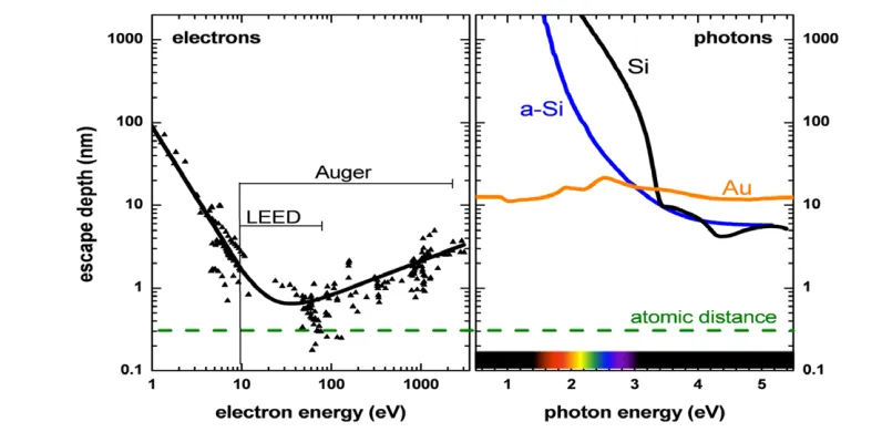
Figure 1 compares sampling depths for electrons with those of photon-based techniques around the visible region of the electromagnetic (EM) spectrum, using the inverse of the absorption coefficient. The figure shows that, even for metals, optical radiation penetrates∼10 nm, allowing buried interfaces to be probed.
Since the first surface optics experiment by Chiarotti
Figure 1. Sampling depths of electron- and photon-based techniques.
the development of elegant optical techniques for interface characterization. This special area of optics has been called epioptics to distinguish from conventional optical spectroscopies [3]. There are reviews available covering different areas of surface and interface optics. A perspective is presented in this paper of recent work and likely future developments in the field.
1.2. The optical response
The interaction of an EM field of optical frequency ω with condensed matter can be described in terms of the polarization amplitude,
P(0, ω,2ω, . . .)=ε0[χ(1)(ω)·E(ω)
+χ(2)(0, ω,2ω):E(ω)E(ω)+ · · ·] (1) where χ(i) is the i th-order dielectric susceptibility tensor describing the material response and only frequency dispersion is shown explicitly. The first term on the right-hand side of the equation describes the linear optical response, which is exploited in conventional techniques like spectroscopic ellipsometry. The dielectric tensor,ε(ω), is related to the linear susceptibility by ε(ω) = 1+χ(1)(ω). The nonlinear terms in the equation become significant at high EM field strengths and the second term in equation (1), which depends on χ(2) and has a polarization quadratic in the EM field, describes the lowest-order nonlinear optical response responsible for optical rectification and second-harmonic generation (SHG). Considering higher nonlinearities briefly within the electric dipole approximation, the third-order response, in the absence of any strong resonantly enhanced surface electric dipole effects, probes the bulk, while the fourth-order response is surface sensitive but requires pulse compression techniques to raise the EM field strength sufficiently to be useful [4].
The linear, second-harmonic and fourth-harmonic optical response are controlled by second rank, third rank and fifth rank tensors, respectively. General symmetry arguments have been used to show that the rank of the tensor and
the order of the multipole expansion of the EM field determines the degree of surface and interface rotational anisotropy that can be probed [5]. Within the electric dipole approximation, an nth rank tensor process can exhibit up to
has been pointed out that epioptic techniques are particularly suited for the in situ characterization of the growth of aligned structures on stepped surfaces, and also for probing buried interfaces and aligned nanostructures that are protected from environmental corrosion or contamination by thin capping layers [10]. It is likely that linear epioptic techniques like RAS will become increasingly used in this technologically important area of advanced materials fabrication.
2. Conventional optical techniques and their
adaptation
Sensitivity and discrimination from the bulk are the two challenges facing conventional optical techniques attempting to probe surface and interface structure [2, 11]. Monolayer resolution can be achieved with some conventional techniques when the response of the interface differs substantially from that of the bulk, as can occur, for example, with some adsorbates.
Diffuse elastic light scattering, also known as laser light scattering, can be used to determine the roughness of thin film surfaces, with atomic-scale resolution in favourable cases [12]. Photoluminescence spectroscopy is widely used to assess material quality in epitaxial semiconductor films grown on low bulk defect substrates, where information on surface and interface quality is available via non-radiative recombination lifetimes. Photoluminescence from nanostructures is also of technological interest, as spatial confinement decreases the non-radiative recombination rate. For example, light emission efficiency from Si1−xGex/Si superlattices is increased by coupling between the nanostructures [13]. Fourier transform infra-red spectroscopy (FTIR) has sufficient sensitivity to probe the vibrational structure of adsorbates at the surfaces of suitable systems, such as small molecules adsorbed on metals [14].
Spectroscopic ellipsometry (SE) is a widely used thin film characterization technique, based on the change in polarization on reflection from the thin film surface. Sub-monolayer resolution can be attained with SE under favourable conditions [2, 11] and the use of SE in characterizing ultra-thin absorbing layers has been reviewed recently [15]. Phenomenological modelling is required if the thickness and dielectric function of the adsorbed layer are to be extracted from the overall response that, for ultra-thin films, is dominated by the bulk response of the substrate.
X-rays can also provide surface and interface information. For example, surface x-ray diffraction (SXRD), which employs grazing incidence to obtain surface sensitivity, can also be used to probe buried interfaces through ultra-thin capping layers [16]. For example, annealing sub-ML amounts of Au deposited on singular and vicinal Si(111) substrates produces
quasi-one-dimensional (1D) single and double Au chain
structures of considerable length [17]. Such ultimate nanowire structures are potentially of technological interest, if they can be capped without significantly perturbing their properties. Recently, SXRD studies of Si(111)-5× 2-Au, capped with 4.6 nm of amorphous Si (a-Si), showed that the positions of the Au atoms under the capping layer were essentially
unchanged [18], raising the interesting possibility of successful capping of this nanowire structure with a-Si. However, RAS studies have shown that the anisotropic optical response of the
(5×2)-Au structure is destroyed during capping, indicating that the technological interesting quasi-1D properties have been lost [19].
Another ray technique of impressive sensitivity is x-ray magnetic circular dichroism (XMCD). The absorption of circularly polarized x-rays in the soft-x-ray energy range is different for parallel and antiparallel orientation of the helicity of the incident light with respect to the magnetization direction of the sample [20]. This synchrotron-based technique can be used to measure the magnetization of ultra-thin ferromagnetic films grown on non-magnetic substrates [21], and was used to show that single atomic wires of Co grown at the step edges of Pt(997) were ferromagnetic at 10 K [22]. The sensitivity of XMCD is significantly greater than that of the magneto-optic Kerr effect (MOKE), which is a form of ellipsometry widely used for ferromagnetic thin film characterization.
2.1. Raman spectroscopy
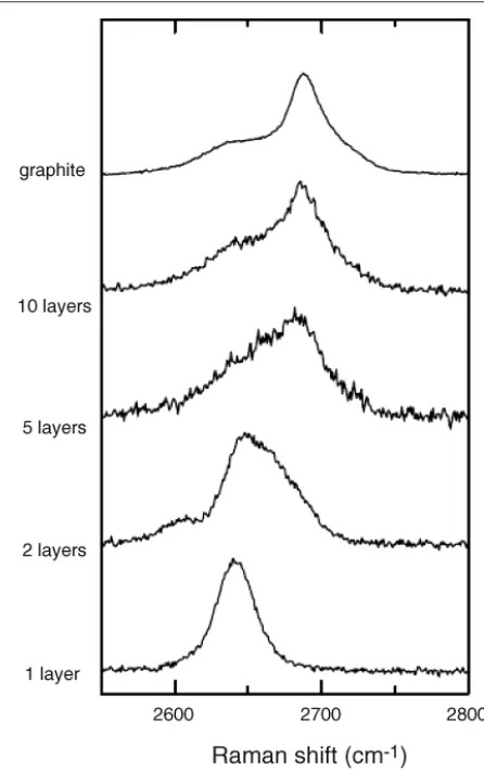
The use of conventional Raman spectroscopy at surfaces has increased recently. Different forms of carbon give strong and distinctive phonon peaks allowing, for example, sp2 and sp3 bonding to be distinguished [23]. Raman spectroscopy and microscopy are now widely used to characterize C60, carbon nanotubes and graphene, where a single carbon layer gives an easily measurable signal (figure2) [24]. Monolayer sensitivity is normally difficult to achieve with Raman spectroscopy unless resonant electronic excitation can be used. The phonon spectra of the zig-zag atomic chains of In on Si(111) have been measured recently (figure3), and major differences were found between the 4×1 phase and the low temperature 8×2 phase below 100 cm−1, which allowed some models of the controversial 8×2 phase to be excluded [25]. The low energy In–In and In–Si vibrations were measured using a triple-grating monochromator and liquid nitrogen cooled CCD array. It is becoming more difficult to source Raman spectrometers capable of accessing this low energy region, as manufacturers appear to be concentrating on producing less costly instruments that use simpler monochromators with notch filters that cut in above 100 cm−1.
Figure 2. Evolution of the Raman spectra of graphene with the
number of layers, using 633 nm excitation. The spectra are normalized to the peak height (adapted from [24]).
SERS is limited in its ability to study molecular adsorption at surfaces in detail because the substrate is typically a poorly characterized, inhomogeneous noble metal. TERS addresses this by replacing the rough metal surface with the sharp metal tip of an atomic force microscope (AFM), thus exploiting the contribution to the SERS response of EM field enhancement in regions of high curvature in an alternative way. TERS is a scanning near-field optical microscopy (SNOM) technique and various laser beam geometries are used to enhance the contrast between the near-field and far-field response. SNOM uses near-field optics to obtain better lateral resolution than is available in conventional, far-field, diffraction-limited images. TERS can probe adsorbed species on well-characterized, homogeneous surfaces with a lateral resolution approaching 10 nm and potential single molecule sensitivity [30]. Figure4 shows the topographical image and TERS spectra of a single-walled carbon nanotube (SWNT) [31]. The TERS spectra have a comparable signal-to-noise ratio to figure1and show changes in the SWNT structure along the length of the tube. There are other SNOM and tip-enhanced SNOM techniques, including nonlinear optical techniques such as coherent anti-Stokes Raman scattering (CARS) and second-harmonic generation (SHG) that are beyond the scope of this paper. It is very likely, however, that SNOM techniques will continue to develop and
mature, and become much more widely used in characterizing nanostructures.
2.2. Surface differential reflectance
Surface differential reflectance (SDR) adapts polarized reflectance measurements to probe surfaces and interfaces by measuring the normalized difference in reflectance when the interface is changed from state a to state b:
Rii
Rii
= Riib −Riia
Ra ii
(2)
where i refers to p-polarized light (EM field vector in the plane of incidence) or s-polarized light (EM field vector orthogonal to the plane of incidence). SDR was used in the earliest surface optics studies where, typically, a clean surface prepared in ultra-high vacuum (UHV) would be oxidized and the change in polarized reflectance measured [1, 32]. The difference in reflectance measures the effect of removing the electronic states of the clean surface on adsorption. The optical transitions of the new adsorbate-induced states typically occur at much higher energies than the spectral region where the clean surface state response is found. Taking the difference removes the bulk contribution, which is unchanged by adsorption. Equation (2) can be expressed in terms of the surface (a), adsorbate-covered surface (b), and bulk dielectric function, typically by using the well-known three-layer model [33]. The bulk dielectric function can be determined using SE, but extracting the components of the surface dielectric function, εii where i = x,y,z, requires knowledge of the response of the adsorbate-covered surface. Often, the latter response will be very similar to that of the bulk. Recent studies of semiconductor surfaces have used hydrogen adsorption, as the H-terminated surfaces are more amenable to ab initio surface optical response calculations [34]. Si(001) surfaces, with their well-known dimer row reconstruction, have been extensively studied and figure5shows experimental results [35], and theoretical SDR results [36] using density functional theory (DFT) within the local density approximation (LDA), for light s-polarized along the[110]and[¯110]directions. Vicinal Si(001) samples were used, offcut 4◦ along [110] to obtain a single domain surface. Figure 5 shows the difference between the clean Si(001)-2×1 surface and the hydrogenated Si(001)-1× 1-H surface, and the theoretical results are blue-shifted rigidly by 0.5 eV to account for the well-known underestimation of excitation energies when self-energy effects are neglected. The spectra essentially are showing the clean surface reflectance as the response of the hydrogenated surface is bulk-like. The reflectance is anisotropic, with a larger response along the dimer rows, which run in the[110]direction. The agreement between theory and experiment is good.
Figure 3. Polarized Raman spectra of Si(111)-4×1-In and Si(111)-8×2-In taken in Aand Asymmetries, using an incident laser energy of 1.91 eV (adapted from [25]).
results [37]. The effective number of electrons that contribute to the surface optical response in a particular spectral region can then be determined from the area under the SDR curves:
neff∝
ω
0
ω[dε(ω)]dω (3)
whereε(ω)is the imaginary part of the dielectric function at frequencyωand d is the nominal surface layer thickness [37]. The SDR spectra depend on the product, dε(ω). Sum rules have been used to show that, below 3.5 eV, the surface optical response of Si(111)-2×1 saturates at one electron per surface atom, consistent with the half-filled dangling bond state of this reconstructed surface [37]. It has also been shown that sum rules can be applied, with care, to RAS spectra [38,39].
3. Linear optical techniques exploiting symmetry:
reflection anisotropy spectroscopy
RAS has proved to be very versatile and is now widely used to study semiconductor and metal single crystal surfaces in UHV, gaseous and electrochemical environments: a comprehensive review has been published recently [40]. RAS measures the difference, at a near-normal angle of incidence, in the reflection
of light polarized along two orthogonal axes x and y in the surface plane, normalized to the mean reflection. The most common experimental arrangement measures the difference,
r , in the complex Fresnel reflection coefficient r
r =2
rx−ry
rx+ry
. (4)
As the anisotropy in the response is generally small, the normalized difference in reflectance R/R ≈ 2 Re(r/r)
and both have been termed RAS signals in the literature. This is essentially a near-normal incidence SE measurement, adapted to measure only the anisotropy in the response. RAS is surface and interface sensitive when the bulk optical response is isotropic, due to the structural symmetry of the bulk, and the symmetry of the surface or interface structure is lower, possessing at the most a two-fold rotation axis. Following SE analysis procedures, simple systems can be described using a three-layer model of isotropic bulk, anisotropic surface or interface layer, and isotropic ambient, giving
r
r =i
2ω
c
d(εxx−εyy)
εb−1
(5)
Figure 4. Three-dimensional topographic image of a single SWNT
on glass and, below, TERS spectra detected at positions 1–4, using 633 nm excitation (adapted from [31]).
dielectric tensor of the anisotropic layer, andεbis the isotropic bulk dielectric function [40]. The quantity d(εxx−εyy)is called the surface dielectric anisotropy and is a robust quantity: in the absence of other information, the division between d and
(εxx−εyy)is uncertain. For more complex multi-layer systems, an analogous approach to that used in SE modelling may be employed.
3.1. Instrumentation
A schematic of the most common phase modulating spectrometer is shown in figure 6. If the optical phase is modulated at frequency f (typically ∼50 kHz), phase-sensitive detection at 2 f measures the real part of equation (4),
while detection at f measures the imaginary part [40]. For in situ studies, strain in the optical window needs to be minimized, particularly if the imaginary part is being measured. Instruments like this are available commercially from a number of manufacturers, with a typical spectral range from 1.5 to 5.0 eV.
Instrumental developments have improved the spectral range, the speed of response and the lateral resolution of the standard instrument. Reflection anisotropy microscopy (RAM) typically uses a fixed wavelength laser source. Figure7 shows recent results from the oxidation of CO on the surface of Pt(110), using an improved design that offers a spatial resolution of <10 μm [41]. Contrast is obtained because adsorption of CO lifts the anisotropic 1×2 reconstruction of the clean and oxygen-covered surface. The video signal of the CCD camera undergoes downstream real-time background subtraction and contrast enhancement, after which the areas of reaction can be seen clearly (figure7(b)).
Expanding the spectral range typically involves using multi-grating monochromators and additional detectors, partic-ularly in the infra-red (IR) region. Calcium fluoride and mag-nesium fluoride tend to be the choice for optical components. For UHV studies, obtaining reliable low-strain windows cov-ering an extended spectral range has proved problematic, but diamond windows may solve this problem and are beginning to become available at manageable prices. Figure8shows recent RAS results in the IR region from Si(111)-2×1 [42]. There has been continuing interest in the(2×1)chain structures of Si(111)and Ge(111)since the first surface optics studies of Chiarotti et al [1]. An unresolved issue is that the combina-tion of photoemission and inverse photoemission results pro-duce a surface state gap of 0.75 eV for Si(111)-2×1, while the measured surface optical gap is 0.45 eV [42]. It appears likely that there is a strong excitonic contribution to the optical gap between dangling bond states on these surfaces. Ab initio calculations of the optical response at surfaces are particularly time-consuming when excitonic effects are included, although progress has recently been reported for Si nanostructures [43]. The optical gap of 0.45 eV in figure8is the same for the intrin-sic and highly doped samples, which eliminates the possibility that the gap narrows on doping because of increased screening. The speed of response of the spectrometer becomes critical when monitoring adsorption and reaction processes in
[image:6.595.128.474.596.731.2]Figure 6. A typical RAS system for in situ studies, employing a photoelastic modulator (PEM) and a low-strain window (adapted from [40]).
Figure 7. Images of the oxidation of CO on Pt(110), using RAM: (a) normal; (b) enhanced contrast. Reproduced with permission from [41]. Copyright 2007 by IOP Publishing Ltd.
real time. Instruments with multi-channel detection have been developed that allow a complete spectrum from 1.4 to 3.2 eV to be gathered in 0.1 s [44], while other instruments have been optimized for in situ monitoring of epitaxial growth [45]. RAS is in routine use for monitoring III–V and II–VI semiconductor growth and, recently, it has been shown that growth monitoring can be extended to organic molecular beam epitaxy [46,47]. RAS studies of pseudomorphic growth of α-quaterthiophene on a tetracene single crystal substrate have shown that the growth is driven by a form of incommensurate epitaxy [48].
3.2. Theoretical developments
The increased computer power that has become available to researchers has made ab initio surface optical response calculations, within the slab model, feasible, although calculating quasiparticle corrections for large unit cells remains expensive. The slab approach is computationally efficient as it restores a periodicity normal to the surface by using a repeating stack of typically ten atomic layers sandwiched between a similar number of vacuum layers [49]. The ab initio approach is based on DFT-LDA and the Car–Parrinello algorithm [50] is used to find the equilibrium geometries of the surface atoms.
The slab polarizabilitiesαii(ω) are calculated and the RAS spectrum can be determined from equation (5) withεii(ω) = 4παii(ω). Within DFT, and neglecting local fields, the slab polarizability is given by
Im[αii(ω)] ∝ 1
ω2Ad
v,c
B Z
|ϕv,k|qi|ϕc,k|2
×δ(Ec−Ev− ¯hω)dk (6)
where v refers to an occupied valence band state of energy
Ev, c refers to an empty conduction band state, qi is the EM wavevector and k the electron wavevector, where the integration is performed over the Brillouin zone, BZ; the surface unit cell is of area A and the slab thickness is
[image:7.595.131.473.306.432.2]Figure 8. Infra-red RAS of highly doped n-type Si(111)-2×1 (full line curve and experimental points), and the spectrum of a nearly intrinsic sample (dashed curve). The vertical scale refers to the doped sample, while the data for the intrinsic material have been
normalized (adapted from [42]).
allow one of the original models of the surface structure to be excluded. This rigid band shift has been applied successfully in comparing theoretical and experimental RAS and SDR spectra of the initial stages of oxidation of Si(001) [54].
The energies of the conduction band states can be corrected, at considerable computational cost, using many-body theory within the GW approximation. This generally produces very good independent quasiparticle (I-QP) band structures and predicts bulk semiconductor band gaps quite accurately. However, for optical transitions the electron– hole interaction and local-field effects should also be taken into account and this requires efficient ways of solving the Bethe–Salpeter equation (BSE) [55]. Results of state-of-the-art calculations are shown in figure 10 for the Si(001)-c4×2 structure, which is the room temperature equilibrium structure where the dimer rows of the Si(001)-2×1 surface are buckled [56].
[image:8.595.55.284.64.367.2]Including the electron–hole interaction clearly shifts the spectral structure at low energies, improving the agreement with experiment but, at higher energies, agreement is not so good, probably because of convergence problems due to the limited sampling of k-space currently possible [56]. It is likely that these sophisticated calculations will become more common, given the increasing interaction between surface optics experimentalists and theoreticians, which is being encouraged by initiatives such as the European Theoretical Spectroscopy Facility (http://www.etsf.eu/).
Figure 9. RAS spectra of Si(111)-4×1-In and the results of DFT-LDA calculations: upper figure, zig-zag chain model; lower figureπ-bonded stacking fault model (adapted from [52]).
Figure 10. Theoretical RAS calculated for Si(001)-c4×2. Solid curves are the I-QP results, while the dashed curves are the BSE results. The experimental data are black dots. The intensity of the theoretical curves is scaled by a factor of five (adapted from [56]).
3.3. Solid–liquid interfaces
[image:8.595.318.536.409.609.2]re-sponse [40]. Metal–electrolyte interfaces are now being ex-plored and, in particular, electrochemically controlled adsorp-tion and desorpadsorp-tion from Au(110) surfaces [57]. This is one of relatively few anisotropic metal substrates that can be prepared under ambient conditions using the flame annealing technique developed and used successfully by electrochemists. An exam-ple of the potential of RAS in exploring this electrochemical interface is a study of the adsorption of the DNA base cytosine and cytidine 5-monophosphate from solutions of NaH2PO4 and K2HPO4 [58]. Ordered structures were formed on the Au surface, and analysis of the RAS results showed that the plane of the nucleic acid base was oriented vertically and was parallel to the[110¯ ]axis of the Au(110) surface. Very recent work, however, has indicated that the extension of this method-ology to the analysis of single stranded DNA hybridization is unlikely to be successful, because the strong interaction of the DNA bases with the Au(110) surface makes them inaccessible. Functionalized diamond surfaces appear to offer more promise for this ambitious project [59]. It is likely that RAS studies of biophysical and biochemical systems at aqueous interfaces will increase significantly in the next few years.
3.4. Nanostructures and solid–solid interfaces
The potential of nanostructures for information and communi-cation technology (ICT) applicommuni-cations is driving a substantial amount of fundamental and applied research. For example, nanowires for interconnects are being intensively studied, par-ticularly single-walled carbon nanotubes. The growth of ori-ented nanowires on Si surfaces is also of interest, being closer to current semiconductor technologies. Such structures are in-trinsically anisotropic and may be characterized using RAS. The aligned quasi-1D single and double atomic chains of Au that can be grown on vicinal Si(111) substrates have been men-tioned previously. RAS is remarkably sensitive to the structure of the atomic chains [19]. Figure11shows the large differ-ence between the single and double chain structures, which are grown on two vicinal substrates offcut by∼9◦, but in opposite directions. The opposite sign of the contribution of the step-induced states [60] is clearly seen at ∼3.3 eV in the figure. The spectral signatures have been used to estimate a 1:2 ratio of single to double chains on 4◦offcut Si(111) [19].
The conductivity of nanowires is a crucial parameter, but electrical contacting to such structures is a major problem, with the contacts often dominating the response of the system. The challenge of growing and contacting aligned conducting nanostructures can be separated by using RAS in the IR spectral region to measure the contactless optical conductivity of the nanostructures. A free carrier, Drude-like response is observed, which can be extrapolated to obtain a DC optical conductivity [61]. Crucially, the effect of capping on nanostructure properties can also be probed [62]. In situ growth monitoring and characterization of aligned nanostructures, and also capping studies and the characterization of the solid– solid interface, are likely to become areas of increased RAS activity.
[image:9.595.318.542.60.227.2]Larger, but still nanoscale, metallic structures are attracting considerable interest because of their potential in
Figure 11. RAS spectra of the single Au chain, Si(557)-5×1-Au structure (−) and the double Au chain, Si(775)-5×2-Au structure (−). Reproduced with permission from [19]. Copyright 2009 by IOP Publishing Ltd.
ICT applications. Current interest is focused on the surface plasmon-polariton resonance, a collective electron motion excited by light. The term plasmonics is used to describe the use of surface plasmon-based circuits to convert micron-scale optical data to nanoscale electronic data [63]. While outside the scope of this overview, it is clear that RAS can contribute to the characterization of such material systems. A recent paper contains a detailed analysis of the origins of the RAS response from Ag nanoparticles supported on an insulating, birefringent substrate. which included the effect of both image states and multipolar resonances [64].
It has been shown recently that RAS can be used to measure the magnetism of thin films and nanostructures, providing spectral MOKE information at near-normal incidence. Although not specifically surface and interface sensitive, and only measuring the normal component of the easy axis response, RAS-MOKE is very sensitive and measures the spectral response [65], in contrast to the single-wavelength laser-based approach necessary for sub-ML sensitivity in conventional MOKE instruments [66]. The growth mode and magnetism of Ni ultra-thin films on Cu(110) substrates using oxygen as a surfactant has been characterized by combining RAS and RAS-MOKE measurements [65]. Given the importance of perpendicular easy axis magnetization structures to ICT, it is likely that RAS-MOKE will see increased use as a characterization tool for magnetic nanostructures.
4. Nonlinear optical techniques exploiting symmetry
The higher rank tensors describing the nonlinear optical response of materials offer more opportunities to exploit symmetry differences. The basis of the surface and interface sensitivity of the main nonlinear epioptic techniques, second-harmonic generation (SHG), sum-frequency generation (SFG) and magnetic second-harmonic generation (MSHG), is that, within the electric dipole approximation, such three-wave mixing phenomena are forbidden in the bulk of centrosymmetric materials. The electric dipole contribution is allowed at the surface or interface, because the symmetry is broken in the direction normal to the interface. These techniques are also sensitive to other factors that affect symmetry, such as surface and interface structure, including step formation, local electric fields and magnetization (MSHG).
For non-magnetic systems, the i th component of the sum-frequency polarization amplitude induced by EM fields of frequencyω1andω2,
Pi(ω1+ω2)=ε0[χi j ks Ej(ω1)Ek(ω2)+χi jlkb Ej(ω1)∇lEk(ω2) +χb
i j kmEj(ω1)Ek(ω2)Em] (7) where χi j ks is the second-order surface dipole tensor component,χb
i jlkis the third-order nonlocal component,χ b i j km is the third-order bulk dipole-allowed component induced by a quasi-static electric field Em, and we have SHG ifω1 =
ω2. Although of higher order, the contribution from the bulk nonlocal quadrupolar term may be comparable in size to the dipolar contribution of the leading term because of the larger sampling volume. The third term, when ω1 = ω2, is called electric-field-induced second-harmonic generation (EFISH). The nonlinear intensity ∝ |Pi|2 and Fresnel coefficients for the fields are required, analogously to linear optics, but for the different incoming and outgoing frequencies and choice of polarizations. The components in equation (7) are generally complex and methods are available for measuring the phase of the optical response [70,71].
Symmetry plays a major role in these nonlinear techniques, as the tensor components reflect the symmetry of the surface or interface. Low symmetry systems have many non-zero components, which can necessitate careful choice of input and output polarizations, and experimental geometry, to simplify the interpretation of results.
4.1. Instrumentation
The development of reliable femtosecond laser systems, based on the Kerr lens mode locking Ti:sapphire laser, was central to the resurgence of interest in the use of nonlinear optics to probe surface and interface structure. The high peak powers necessary to obtain a significant nonlinear response can be combined with a low average power to avoid damage or even significant heating of the interfacial region. Probing electronic resonances is clearly important and the relatively narrow spectral range available can be expanded, for example, by using an optical parametric amplifier. A difference frequency generator can be used with amplified pulses to provide access
to ∼10μm. Conventional widely tuneable systems operate at∼1 kHz repetition rates, but high repetition rate systems, operating at ∼100 kHz, are now available that can offer improved reliability. The cost of these systems can be prohibitive, however, and super continuum sources, based on nonlinear high power fibre amplifiers, are beginning to offer a more cost-effective approach for standard applications, delivering high peak power typically between ∼350 nm and
∼2.5μm with picosecond pulses at megahertz repetition rates. SFG overlaps two beams at the interface, generally one from a fixed visible source and one from a tuneable IR source, to probe interface vibrational resonant structure by detecting the sum-frequency in the visible region. An efficient approach developed about ten years ago uses pulse shaping to combine long, and thus spectrally narrow, visible pulses with short, spectrally broad IR pulses to obtain single-shot SFG using a spectrograph and CCD camera [72]. Electronic and vibrational double-resonance experiments are beginning to appear using free-electron lasers and optical parametric oscillators [73].
4.2. Theory
The challenges facing surface and interface ab initio linear optical response calculations were discussed in section 3.2. Ab initio nonlinear calculations are even more computationally expensive, involving additional summations over intermediate states, and even bulk calculations have had limited success [74]. Alternative theoretical approaches have been reviewed [75] and, recently, interest has increased in polarizable dipole [76] and polarizable bond [77] models of the nonlinear optical response. Aspnes and co-workers have proposed a simplified bond hyperpolarizability model, where it was assumed that only the axial component of the bond hyperpolarizability contributes to the nonlinear response [78], and have recently extended this by including transverse components and higher-order effects [79]. The far-field SH radiation at a distance r from the SH dipoles is
E(2ω)=k 2eikr
r [ ˆI− ˆkkˆ]·
N
n=1
j
pn
j (8)
whereIˆis the unit tensor, kˆ is a unit vector in the direction of the observer and the summations are over the unit cells and the different bonds within the unit cell. The axial SH dipole moments of an individual bond
pj =βjbˆjbˆjbˆj·E(ω)E(ω) (9)
4.3. Second-harmonic generation and EFISH
SHG is sensitive to surface and interface symmetry, and many experiments have exploited this. Extensive reviews of the application of SHG to semiconductor [82] and molecular interfaces have been published [83]. Continuing the discussion of bond models, vicinal Si(001)/SiO2 interfaces have been probed by SHG and RAS in the same spectral range, and a simplified bond model used to analyse the results. Miller’s rule was used to generate axial linear polarizabilities and linear spectra from the hyperpolarizabilities obtaining by fitting the SHG response. It was found that the linear spectra reproduced the experimental RAS results quite well [80]. This is promising, as it appears these simple models may provide a guide to interpreting the optical response of quite complicated interfaces, such as the step and terrace structure of these vicinal systems. It also underlines the importance of applying complementary epioptic techniques, such as RAS and SHG, to complex systems.
SHG from well-characterized surfaces in UHV continues to be published, often being used to exclude models of the surface structure that do not possess the in-plane symmetry revealed by SHG via either sample or polarization rotation plots [2]. A recent example is the Si(111)-3 × 1-Ag surface structure, which SHG shows not to possess a mirror plane [84, 85]. When a vicinal Si(111) substrate is used to force a single domain structure, an x z mirror plane is retained orthogonal to the steps andα-sx polarization rotation plots of the clean surface show a four-fold symmetry. The top plot in figure12shows that the formation of the 3×1-Ag structure breaks this symmetry, confirming the absence of the mirror plane.
RAS has been widely used for compound semiconductor epitaxial growth monitoring, but is not generally suited to characterizing Si and Ge growth, due to domain averaging on Si(001) and the three-fold symmetry of Si(111). Recently, SHG has been investigated for the real-time monitoring of the growth of hydrogenated amorphous Si, using both the polarization and spectral dependence of the SHG signal, with promising results [86–88].
Also of interest in semiconductor technology is the use of EFISH to probe the electric fields, and thus the charge properties, at the buried Si/SiO2 interface [82]. Extracting the complex EFISH contribution to the nonlinear response is simplified by measuring the EFISH phase shift, as has been demonstrated for a Cr/SiO2/Si MOS structure [89]. Recently, high-κ dielectric interfaces have been investigated and it has been shown that SHG can be used to monitor the effect of composition and annealing on the fixed charge at Si/SiO2/Hf1−xSixO2 interfaces [90]. Band offsets can also be measured using pump–probe techniques, as discussed in section4.6[91].
[image:11.595.320.538.74.334.2]Strain is another symmetry-breaking phenomenon and SHG has been used to probe strain in a variety of material systems, including at semiconductor interfaces [82]. In many of these studies the strain arises from a lattice mismatch that produces a strain that is not amenable to external control. Recently, controlled measurements of the SHG strain response in a capped Co0.25Pd0.75 alloy film have been made
Figure 12. SHG polarization rotation plots for Si(111)-3×1-Ag, whereαis the input polarization angle. The top plot shows the breaking of mirror plane symmetry (adapted from [85]).
by growing it on a lead zirconate titanate thin film and using the inverse piezoelectric effect to control the applied stress [92]. The analysis is quite complicated, but indicates how ferroelectric polarization can be treated. Given the technological importance of ferroelectric interfaces, there is likely to be an increase in SHG studies of these material systems.
Studies of chirality using optics are particularly important in biochemical and biophysical systems, and interest in optically active chiral nanoparticles has also increased recently [93]. SHG can be used to detect chirality via the response of theχxyztensor component and can detect adsorbed monolayers under favourable conditions. SHG studies of chiral molecules [94] and surface systems [95] have been reviewed recently. In principle, RAS is also capable of detecting chirality, but it is not yet clear whether it has sufficient sensitivity. In an interesting very recent study of a Langmuir monolayer, an achiral molecule, 5-octadecyloxy-2-(2-pyridylazo)phenol, was shown to form chiral aggregates spontaneously on aggregation, probably due to the formation of local twist structures [96]. It has also been shown that tuning into excitonic resonances can produce a large increase in the SHG chiral response [97]. It remains to be seen whether the use of amplified pulses and/or resonant enhancement will allow the detection of sub-monolayer quantities of small chiral molecules at surfaces and interfaces.
4.4. Sum-frequency generation
to probe vibrational structure at surface and interfaces. The main advantage of SFG is the increased surface sensitivity available, compared to conventional IR spectroscopies, arising from detection at the sum-frequency wavelength, which allows the use of much more sensitive detectors operating in or near the visible region. Other advantages include a background-free signal and the time resolution associated with short laser pulses. Comprehensive reviews of SFG have been published recently [98,99].
SFG is mostly used for probing molecular vibrations at surfaces and interfaces, but some surface phonon work has been reported. It has been pointed out recently that SFG is not sensitive to the Fuchs–Kliewer surface phonon-polaritons that tend to dominate electron energy-loss spectra, but is sensitive to the microscopic surface phonons that are more characteristic of the surface structure [100]. Two surface vibrational modes ofα-quartz arising from Si–O–Si and Si–OH structures have been identified.
Arguably the most important hydroxyl structures are those at water interfaces. SFG studies are continuing to contribute significantly to the understanding of water–vapour interface structures and the role of hydrogen bonding, after pioneering SFG work from Shen and co-workers about ten years ago [101]. Recently, phase-sensitive SFG techniques have been developed that provide unique information about the net polar orientations of water species at interfaces [102,103]. Isotopic substitution has also been used to explore the hydrogen bond strengths at different water interfaces and to resolve a recent controversy. Figure 13 shows the disappearance of the well-known double peak structure on isotopic dilution, providing good evidence that this originates from intramolecular coupling at the interface rather than from ‘ice-like’ and ‘liquid-like’ water [104,105]. The figure also shows the impressive SNR possible with SFG.
The data from the water–lipid interface in figure13are an example of an area where increased activity may be expected. The water interface at the molecular level is critical to the understanding of biochemical and biophysical processes. Very recently SFG has been used to probe a monolayer of a model lung surfactant, comprising four lipids and a protein [106].
Electrolyte interfaces are another class of aqueous interfaces that have been extensively studied by SFG. Recently, access to free-electron lasers has allowed two-colour, doubly-resonant studies to be undertaken, with improved spectral and temporal resolution compared to tabletop systems [73,107]. This is another area that is likely to develop further as new large-scale facilities come on stream.
4.5. Magnetic second-harmonic generation
[image:12.595.319.540.66.275.2]Magnetic interfaces and nanostructures are attracting consider-able current interest, both regarding the fundamental physics and in their technological application [108]. As discussed above, a key advantage of photon-in/photon-out techniques is their ability to probe buried nanostructures located in the inter-facial region between the substrate and the capping layer used to protect the nanostructure from environmental corrosion and contamination [2]. However, techniques such as MOKE and
Figure 13. SFG spectra at different isotopic ratios of D/H at
aqueous interfaces with silica, a lipid, and air. Filled squares: deuterium ratio D/(D+H)=1; circles D/(D+H)=0.33. Lines are fits to the spectra, which are offset for clarity (adapted
from [105]).
XMCD have difficulty in discriminating between bulk and in-terface effects, or between inin-terface and step contributions in aligned magnetic nanostructures. MSHG extends the surface and interface sensitivity of SHG to magnetic interfaces. Mag-netization, as an axial vector, does not lift the inversion sym-metry of the bulk, allowing magnetic surfaces and interfaces to be probed in the presence of bulk magnetism. With the de-velopment of reliable femtosecond lasers, MSHG surface and interface studies became relatively straightforward, due to the improvement in the signal-to-noise ratio (SNR).
Within the electric dipole approximation, the intensity of MSHG from a magnetic interface is given by
I(2ω; ±M)∝ |χeffevenE(ω)E(ω)±χeffoddME(ω)E(ω)|2 (10) where χeffeven is the effective second-order crystallographic susceptibility tensor, E(ω) is the input electric-field vector,
χeff
odd is the effective third-order axial magnetic susceptibility tensor and M is the interface magnetization. Higher-order quadrupolar crystallographic contributions from the substrate or capping layer can be included in the effective value of the even term. SHG is sensitive to strain and any magneto-elastic contributions will appear in the even term. Appropriate Fresnel and local electromagnetic field factors are included in the effective tensor components of equation (10). For high symmetry interfaces, input and output polarizations can be chosen to identify even and odd components. The size of the odd contribution is typically∼10% of the even contribution. A comprehensive review of MSHG has been published recently by Kirilyuk and Rasing [109].
Figure 14. Normalized|χodd
eff|for the pin/soutgeometry as a function of the deposited Fe thickness on the Fe(001)- p1×1-O system (adapted from [110]).
bulk magnetism of the centrosymmetric Fe(001) substrate and only measures the surface magnetism, where the inversion symmetry is broken. A monolayer of oxygen acts as a surfactant in the homoepitaxial growth of Fe films on Fe(001), floating on the top of the growing film. The oscillations in MSHG intensity were attributed to the 7% outward relaxation of the top Fe layer, which is expected to increase the magnetic moment of the Fe atoms in the surface layer. Exchange-biased magnetic interfaces have also been probed successfully [111–113]. Magnetic oxide interfaces can also be probed. MSHG has been used to characterize the local magnetic properties at the interface of a perovskite ferromagnet, as used in spin-tunnel junctions [114]. The magnetic properties of interfaces of antiferromagnetic oxide films are also attracting interest [115] and MSHG can also probe these structures [116].
Work so far has been largely restricted to interfaces with high in-plane symmetry, due to the large number of tensor components that can contribute to lower symmetry magnetic systems [109]. Experimental geometries have also been chosen to ensure that the effective odd contribution remains small compared to the even contribution, allowing the expression for the MSHG contrast to be linearized:
A= I
+−I−
I++I− ≈2
|χeff oddM| |χeff
even|
cosθ (11)
where the +/− superscript refers to equal but opposite magnetizations and θ is the phase difference between the odd and even components [110, 113, 117]. Equation (11) shows that, if the effective even and odd components either remain constant or vary in the same way in an experiment, the asymmetry is proportional to the magnetization.
The main contributions to variation in the tensor components with coverage are expected to come from changes in the local electronic structure and the local electromagnetic fields at the interface. Edge or step contributions are likely to be different to those of the islands or terrace [113]. Indeed, MOKE studies from magnetic
films grown on vicinal substrates have reported distinct step effects at higher vicinal angles [118–120]. Step or edge contributions become increasingly important in the magnetism of aligned nanostructures as their dimensions shrink. Self-assembly at atomic steps has proved to be a useful route to aligned structures, with two well studied systems being vicinal W(110)/Fe, where MOKE was used to measure the magnetization of sub-monolayer nanostripes as small as ten atoms in width [121], and Pt(997)/Co, where the magnetization of single atomic wires was measured using XMCD, as discussed above [22].
A major attraction of applying MSHG to aligned magnetic nanostructures is that the symmetry of the edges or steps is lower than that of the terraces or islands and this, in principle, allows their contribution to be distinguished by MSHG [122]. However, two major difficulties must be overcome: sensitivity and complexity. A recent approach to overcoming the former is to account properly for the quadratic magnetic response implicit in equation (10), rather than using an experimental configuration that produces a smaller magnetic response in order to use the linearized expression of equation (11) [123]. Without this constraint, a large value of the contrast can be chosen, which increases the SNR.
Regarding complexity, lower symmetry systems have many tensor components that may contribute to the MSHG intensity, making interpretation particularly difficult where there are multiple magnetic regions. Recently, it has been shown that normal incidence (NI) SHG geometry makes the response manageable by excluding z-dependent tensor components, while choosing a large value of the contrast compensates for the reduced signal associated with the geometry [124].
For a typical vicinal system, a single x z mirror plane is retained perpendicular to the steps. For different magnetic regions, n, the dependence of the y-polarized NI MSHG intensity onϕ, the angle between the input polarization field and the x -direction, is given by:
Iy(2ω;ϕ,±MX)∝ |
n
yx y(n)sin 2ϕ
± {yx x X(n)cos2ϕ+yyy X(n)sin2ϕ}MX(n)|2 (12) where the odd magnetic tensor componentχi j kL ≡i j k L etc, and the magnetization is in direction L. Equation (12) contains only three tensor components for each magnetic region and can be used when the easy axis is in the x direction in the plane of the interface. MSHG thus offers the important diagnostic capability of exploiting the properties of the optical tensor components to identify different magnetization contributions from inhomogeneous interfaces and nanostructures, because the components will vary with the local atomic structure.
Figure 15. Extracted centrosymmetric hysteresis loops for vicinal W(110)/Fe/15 nm Au, for input polarization angles near 0◦and 90◦(or symmetry-related positions), together with the magnetic contrast as a function of temperature. Solid lines are simultaneous fits to all sets of data for a given coverage. Left column: 0.25 ML Fe. Right column: 3 ML Fe.
with the lower W/Fe interface and the upper Fe/Au interface. This experimental approach opens up low symmetry magnetic interfaces and aligned nanostructures to characterization by MSHG.
4.6. Temporal studies
The short pulse laser systems needed to obtain the power densities necessary for nonlinear optics at surfaces and interfaces are also readily used for temporal studies and a significant amount of work has been published. Only a few recent examples can be mentioned in this overview. SHG spectral hole burning in the dangling bond states of Si(111)-7×7, using 100 fs pulses, revealed strong coupling between these localized surface states and a surface phonon mode [126]. Pump–probe techniques are also used to measure slower processes. Band offsets at Si/SiO2 interfaces have been measured with two-colour pump–probe, time-dependent EFISH. Electrons are optically pumped into the oxide and trapped, and the EFISH response measured. The pumping rates, and thus the electric field and EFISH signal, vary with the order of the multiphoton process, which depends on the photon energy. Tuning the pump beam then allows thresholds for the internal photoemission process to be identified and band offsets measured [91].
Pump–probe techniques are also being used in SFG studies. At the air–water interface, SFG with an additional pump beam has been used to measure ultra-fast
vibrational energy transfer between surface and bulk water molecules [127].
5. Conclusion
A perspective of recent work in the area of surface and interface optics has been presented. The understanding gained from studies of well-characterized systems under UHV conditions has led to epioptic techniques being used with increasing confidence to probe solid–gas, solid–liquid and solid–solid interfaces. Aqueous and electrolytic interfaces are of particular interest and the first studies of biochemical and biophysical interfacial systems have appeared. The future is likely to see a major increase in the use of epioptics to probe these solid– liquid interfaces, and also the solid–solid interfaces of interest in ICT and nanotechnology.
Acknowledgment
This publication has emanated from research conducted with the financial support of Science Foundation Ireland.
References
[1] Chiarotti G, del Signore G and Nannarone S 1968 Phys. Rev.
Lett.21 1170
[2] McGilp J F 1995 Prog. Surf. Sci.49 1
[5] Koopmans B, van der Woude F and Sawatzky G A 1992 Phys.
Rev. B46 12780
[6] Lee Y S and Downer M C 2000 Thin Solid Films364 80 [7] McGrath R, Smerdon J A, Sharma H R, Theis W and
Ledieu J 2010 J. Phys.: Condens. Matter22 084022 [8] Lifshitz R, Arie A and Bahabad A 2005 Phys. Rev. Lett.
95 133901
[9] Hawkeye M M and Brett M J 2007 J. Vac. Sci. Technol. A 25 1317
[10] McGilp J F 2001 Phys. Status Solidi a188 1361
[11] Bordo V G and Rubahn H-G 2005 Optics and Spectroscopy at
Surfaces and Interfaces (Weinheim: Wiley–VCH)
[12] Chu B 1991 Laser Light Scattering (New York: Academic) [13] Tayagaki T, Fukatsu S and Kanemitsu Y 2009 Phys. Rev. B
79 041301
[14] Hirschmugl C J 2002 Surf. Sci.500 577
[15] Hilfiker J N, Singh N, Tiwald T, Convey D, Smith S M, Baker J H and Tompkins H G 2008 Thin Solid Films 516 7979
[16] Robinson I K and Tweet D J 1992 Rep. Prog. Phys.55 599 [17] Crain J N, McChesney J L, Zheng F, Gallagher M C,
Snijders P C, Bissen M, Gundelach C, Erwin S C and Himpsel F J 2004 Phys. Rev. B69 125401
[18] Iwasawa Y, Voegeli W, Shirasawa T, Sekiguchi K, Nojima T, Yoshida R, Takahashi T, Matsumoto M, Okano T, Akimoto K, Kawata H and Sugiyama H 2008 Appl. Surf.
Sci.254 7803
[19] McAlinden N and McGilp J F 2009 J. Phys.: Condens. Matter at press
[20] Chen C T, Sette F, Ma Y and Modesti S 1990 Phys. Rev. B 42 7262
[21] Gambardella P 2003 J. Phys.: Condens. Matter15 S2533 [22] Gambardella P, Dallmeyer A, Malti K, Malagoli M C,
Eberhardt W, Kern K and Carbone C 2002 Nature416 301 [23] Ferrari A C and Robertson J 2000 Phys. Rev. B61 14095 [24] Ferrari A C, Meyer J C, Scardaci V, Casiraghi C, Lazzeri M,
Mauri F, Piscanec S, Jiang D, Novoselov K S, Roth S and Geim A K 2006 Phys. Rev. Lett.97 187401
[25] Fleischer K, Chandola S, Esser N, Richter W and McGilp J F 2007 Phys. Rev. B76 205406
[26] Wu D-Y, Li J-F, Ren B and Tian Z-Q 2008 Chem. Soc. Rev. 37 1025
[27] Banholzer M J, Millstone J E, Qin L and Mirkin C A 2008
Chem. Soc. Rev.37 885
[28] Lal S, Grady N K, Kundu J, Levin C S, Lassiter J B and Halas N J 2008 Chem. Soc. Rev.37 898
[29] Pieczonka N P W and Aroca R F 2008 Chem. Soc. Rev. 37 946
[30] Bailo E and Deckert V 2008 Chem. Soc. Rev.37 921
[31] Hartschuh A, S´anchez E J, Xie X S and Novotny L 2003 Phys.
Rev. Lett.90 095503
[32] Chiaradia P and Sole R D 1999 Surf. Rev. Lett.6 517 [33] McIntyre J D E and Aspnes D E 1971 Surf. Sci.24 417 [34] Borensztein Y 2005 Phys. Status Solidi a202 1313 [35] Borensztein Y and Witkowski N 2004 J. Phys.: Condens.
Matter16 S4301
[36] Kress C, Shkrebtii A and Del Sole R 1997 Surf. Sci. 377–379 398
[37] Chiarotti G, Chiaradia P, Faiella E and Goletti C 2000 Surf.
Sci.453 112
[38] Chiarotti G, Chiaradia P, Arciprete F and Goletti C 2001 Appl.
Surf. Sci.175/176 777
[39] Goletti C, Bussetti G, Chiaradia P and Chiarotti G 2004
J. Phys.: Condens. Matter16 S4289
[40] Weightman P, Martin D S, Cole R J and Farrell T 2005 Rep.
Prog. Phys.68 1251
[41] Punckt C, Merkt F S and Rotermund H H 2007 New J. Phys. 9 213
[42] Bussetti G, Goletti C, Chiaradia P and Chiarotti G 2005 Phys.
Rev. B72 153316
[43] Bruno M, Palummo M, Marini A, Del Sole R and Ossicini S 2007 Phys. Rev. Lett.98 036807 [44] Harrison P, Farrell T, Maunder A, Smith C I and
Weightman P 2001 Meas. Sci. Technol.12 2185 [45] Kaspari C, Pristovsek M and Richter W 2005 Phys. Status
Solidi b242 2561
[46] Goletti C, Bussetti G, Chiaradia P, Sassella A and Borghesi A 2003 Appl. Phys. Lett.83 4146
[47] Sassella A, Campione M, Moret M, Borghesi A, Goletti C, Bussetti G and Chiaradia P 2005 Phys. Rev. B71 201311 [48] Sassella A, Campione M, Raimondo L, Borghesi A,
Bussetti G, Cirilli S, Violante A, Goletti C and Chiaradia P 2009 Appl. Phys. Lett.94 073307 [49] Inglesfield J E 1982 Rep. Prog. Phys.45 223 [50] Car R and Parrinello M 1985 Phys. Rev. Lett.55 2471 [51] Manghi F, Del Sole R, Selloni A and Molinari E 1990 Phys.
Rev. B41 9935
[52] Fleischer K, Chandola S, Esser N, Richter W, McGilp J F, Schmidt W G, Wang S, Lu W and Bernholc J 2004 Appl.
Surf. Sci.234 302
[53] Wippermann S and Schmidt W G 2009 Surf. Sci.603 247 [54] Gaal-Nagy K, Incze A, Onida G, Borensztein Y,
Witkowski N, Pluchery O, Fuchs F, Bechstedt F and Del Sole R 2009 Phys. Rev. B79 045312
[55] Palummo M, Pulci O, Sole R D, Marini A, Hahn P, Schmidt W G and Bechstedt F 2004 J. Phys.: Condens.
Matter16 S4313
[56] Palummo M, Witkowski N, Pluchery O, Del Sole R and Borensztein Y 2009 Phys. Rev. B79 035327
[57] Sheridan B, Martin D S, Power J R, Barrett S D, Smith L C, Lucas C A, Nichols R J and Weightman P 2000 Phys. Rev.
Lett.85 4618
[58] Weightman P, Dolan G J, Smith C I, Cuquerella M C, Almond N J, Farrell T, Fernig D G, Edwards C and Martin D S 2006 Phys. Rev. Lett.96 086102 [59] Smith C I, Bowfield A, Cuquerella M C, Mansley C P,
Farrell T, Harrison P, Martin D S, Fernig D G, Edwards C, Butler J E, Hamers R J, Sun B, Wang X and
Weightman P 2009 Europhys. Lett.85 18006
[60] Schmidt W G, Bechstedt F and Bernholc J 2001 Phys. Rev. B 63 045322
[61] Fleischer K, Chandola S, Herrmann T, Esser N,
Richter W and McGilp J F 2006 Phys. Rev. B74 195432 [62] Fleischer K, Jacob J, Chandola S, Esser N and McGilp J F
2008 Phys. Status Solidi c5 2556 [63] Ozbay E 2006 Science311 189
[64] Flores-Camacho J M, Sun L D, Saucedo-Zeni N, Weidlinger G, Hohage M and Zeppenfeld P 2008 Phys.
Rev. B78 075416
[65] Herrmann T, Ludge K, Richter W, Georgarakis K G, Poulopoulos P, Nunthel R, Lindner J, Wahl M and Esser N 2006 Phys. Rev. B73 134408
[66] Bader S D 1991 J. Magn. Magn. Mater.100 440 [67] R¨onnow D, Lastras-Mart´ınez L F, Cardona M and
Santos P V 1999 J. Opt. Soc. Am. A16 568 [68] Liarokapis E, Papadimitriou D, Rumberg J and
Richter W 1999 Phys. Status Solidi b211 309 [69] Lastras-Mart´ınez L F, Ortega-Gallegos J,
Balderas-Navarro R E, Flores-Camacho J M, Chavira-Rodr´ıguez M E, Lastras-Mart´ınez A and Cardona M 2008 Phys. Status Solidi c5 2591
[70] Veenstra K J, Petukhov A V, De Boer A P and Rasing T 1998
Phys. Rev. B58 R16020
[71] Wilson P T, Jiang Y, Aktsipetrov O A, Mishina E D and Downer M C 1999 Opt. Lett.24 496
[72] Richter L J, Petralli-Mallow T P and Stephenson J C 1998
Opt. Lett.23 1594
[73] Bozzini B, D’Urzo L, Mele C, Busson B, Humbert C and Tadjeddine A 2008 J. Phys. Chem. C112 11791 [74] Bergfeld S and Daum W 2003 Phys. Rev. Lett.90 036801 [75] Downer M C, Mendoza B S and Gavrilenko V I 2001 Surf.
[76] Arzate N, Mendoza B S and Vazquez-Nava R A 2004
J. Phys.: Condens. Matter16 S4259
[77] Patterson C H, Weaire D and McGilp J F 1992 J. Phys.:
Condens. Matter4 4017
[78] Powell G D, Wang J F and Aspnes D E 2002 Phys. Rev. B 65 205320
[79] Adles E J and Aspnes D E 2008 Phys. Rev. B77 165102 [80] Kwon J, Downer M C and Mendoza B S 2006 Phys. Rev. B
73 195330
[81] McGilp J F 2007 J. Phys.: Condens. Matter 19 13 pp [82] L¨upke G 1999 Surf. Sci. Rep.35 75
[83] Zhang W, Wang H and Zheng D 2006 Phys. Chem. Chem.
Phys.8 4041
[84] Deng D and Suzuki T 2004 Japan. J. Appl. Phys. 243 510 [85] Jacob J, Gomes Silva A, Fleischer K and McGilp J F 2008
Phys. Status Solidi c5 2649
[86] Kessels W M M, Gielis J J H, Aarts I M P, Leewis C M and van de Sanden M C M 2004 Appl. Phys. Lett.85 4049 [87] Aarts I M P, Gielis J J H, van de Sanden M C M and
Kessels W M M 2006 Phys. Rev. B73 045327 [88] Gielis J J H, Gevers P M, Aarts I M P,
van de Sanden M C M and Kessels W M M 2008 J. Vac.
Sci. Technol. A26 1519
[89] Dolgova T V, Fedyanin A A and Aktsipetrov O A 2003 Phys.
Rev. B68 073307
[90] Carriles R, Kwon J, An Y Q, Miller J C, Downer M C, Price J and Diebold A C 2006 Appl. Phys. Lett.88 161120 [91] Marka Z, Pasternak R, Rashkeev S N, Jiang Y, Pantelides S T,
Tolk N H, Roy P K and Kozub J 2003 Phys. Rev. B 67 45302
[92] Jeong J-W, Shin S-C, Dadoenkova N N, Lyubchanskii I L, Valev V K and Rasing T 2007 Appl. Phys. Lett.90 044108 [93] Noguez C and Garzon I L 2009 Chem. Soc. Rev.38 757 [94] Fischer P and Hache F 2005 Chirality17 421
[95] Hicks J M and Petralli-Mallow T 1999 Appl. Phys. B68 589 [96] Xu Y-Y, Rao Y, Zheng D-s, Guo Y, Liu M-h and
Wang H-F 2009 J. Phys. Chem. C113 4088
[97] Schanne-Klein M C, Boulesteix T, Hache F, Alexandre M, Lemercier G and Andraud C 2002 Chem. Phys. Lett. 362 103
[98] Vidal F and Tadjeddine A 2005 Rep. Prog. Phys.68 1095 [99] Hopkins A J, McFearin C L and Richmond G L 2005 Curr.
Opin. Solid State Mater. Sci.9 19
[100] Liu W-T and Shen Y R 2008 Phys. Rev. Lett.101 016101 [101] Du Q, Freysz E and Shen Y R 1994 Science264 826 [102] Ostroverkhov V, Waychunas G A and Shen Y R 2005 Phys.
Rev. Lett.94 046102
[103] Ji N, Ostroverkhov V, Tian C S and Shen Y R 2008 Phys. Rev.
Lett.100 096102
[104] Sovago M, Campen R K, Wurpel G W H, Muller M, Bakker H J and Bonn M 2008 Phys. Rev. Lett.100 173901 [105] Sovago M, Kramer Campen R, Bakker H J and Bonn M 2009
Chem. Phys. Lett.470 7
[106] Ghosh A, Campen R K, Sovago M and Bonn M 2009 Faraday
Discuss.141 145
[107] Humbert C, Busson B, Six C, Gayral A, Gruselle M, Villain F and Tadjeddine A 2008 J. Electroanal. Chem. 621 314
[108] Velev J P, Dowben P A, Tsymbal E Y, Jenkins S J and Caruso A N 2008 Surf. Sci. Rep.63 400
[109] Kirilyuk A and Rasing T 2005 J. Opt. Soc. Am. B22 148 [110] Nyvlt M, Bisio F, Franta J, Gao C L, Petek H and
Kirschner J 2005 Phys. Rev. Lett.95 127201 [111] Sampaio L C, Mougin A, Ferre J, Georges P, Brun A,
Bernas H, Poppe S, Mewes T, Fassbender J and Hillebrands B 2003 Europhys. Lett.63 819
[112] Valev V K, Gruyters M, Kirilyuk A and Rasing T 2006 Phys.
Rev. Lett.96 067206
[113] Valev V K, Kirilyuk A, Longa F D, Kohlhepp J T,
Koopmans B and Rasing T 2007 Phys. Rev. B75 012401 [114] Yamada H, Ogawa Y, Ishii Y, Sato H, Kawasaki M,
Akoh H and Tokura Y 2004 Science305 646
[115] Finazzi M, Duo L and Ciccacci F 2007 Surf. Sci. Rep.62 337 [116] Pisarev R V, Sanger I, Petrakovskii G A and Fiebig M 2004
Phys. Rev. Lett.93 037204
[117] Straub M, Vollmer R and Kirschner J 1996 Phys. Rev. Lett. 77 743
[118] Choi H J, Qiu Z Q, Pearson J, Jiang J S, Li D and Bader S D 1998 Phys. Rev. B57 12713
[119] Choi H J, Kawakami R K, Escorcia-Aparicio E J, Qiu Z Q, Pearson J, Jiang J S, Dongqi L and Bader S D 1999 Phys.
Rev. Lett.82 1947
[120] Choi H J, Kawakami R K, Escorcia-Aparicio E J, Qiu Z Q, Pearson J, Jiang J S, Li D, Osgood R M III and Bader S D 1999 J. Appl. Phys.85 4958
[121] Hauschild J, Elmers H J and Gradmann U 1998 Phys. Rev. B 57 R677
[122] Carroll L and McGilp J F 2003 Phys. Status Solidi c0 3046 [123] McGilp J F, Carroll L and Fleischer K 2007 J. Phys.:
Condens. Matter19 396002
[124] Carroll L, Fleischer K, Cunniffe J P and McGilp J F 2008
J. Phys.: Condens. Matter20 265002
[125] McGilp J F, Carroll L, Fleischer K, Cunniffe J P and Ryan S 2009 J. Magn. Magn. Mater. at press (doi:10.1016/j.jmmm.2009.03.081)
[126] McGuire J A, Raschke M B and Shen Y R 2006 Phys. Rev.
Lett.96 087401
[127] Smits M, Ghosh A, Sterrer M, Muller M and Bonn M 2007
![Figure 3. Polarized Raman spectra of Si(111)-41.91 eV (adapted from [ × 1-In and Si(111)-8 × 2-In taken in A′ and A′′ symmetries, using an incident laser energy of25]).](https://thumb-us.123doks.com/thumbv2/123dok_us/1496836.690226/5.595.147.459.67.426/figure-polarized-raman-spectra-adapted-symmetries-incident-energy.webp)
![Figure 5. Experimental s-polarized SDR spectra, for light polarized along two orthogonal axes in the surface plane (adapted from [34]),compared with DFT-LDA calculations (adapted from [36]).](https://thumb-us.123doks.com/thumbv2/123dok_us/1496836.690226/6.595.60.280.67.348/figure-experimental-polarized-polarized-orthogonal-compared-calculations-adapted.webp)
![Figure 6. A typical RAS system for in situ studies, employing a photoelastic modulator (PEM) and a low-strain window (adapted from [40]).](https://thumb-us.123doks.com/thumbv2/123dok_us/1496836.690226/7.595.131.473.306.432/figure-typical-studies-employing-photoelastic-modulator-strain-adapted.webp)
![Figure 9. RAS spectra of Si(111)-4 × 1-In and the results ofDFT-LDA calculations: upper figure, zig-zag chain model; lowerfigure π-bonded stacking fault model (adapted from [52]).](https://thumb-us.123doks.com/thumbv2/123dok_us/1496836.690226/8.595.318.536.409.609/figure-spectra-results-calculations-gure-lowergure-stacking-adapted.webp)


![Figure 14. Normalizedof the deposited Fe thickness on the Fe(001)-(adapted from [ |χoddeff | for the pin/sout geometry as a functionp1 × 1-O system110]).](https://thumb-us.123doks.com/thumbv2/123dok_us/1496836.690226/13.595.56.282.60.238/figure-normalizedof-deposited-thickness-adapted-xoddeff-geometry-functionp.webp)