Bachelor Assignment
Computational Material Sciences
-Interface Models for Spin Transport through
Magnetic Multilayers
Author: Bas Schuttrups
Contents
1 Introduction 3
2 Theory 5
2.1 Valet-Fert . . . 5
2.1.1 Change of variables . . . 6
2.2 Transfer Matrices . . . 7
2.3 Interface Models . . . 8
2.3.1 Valet-Fert . . . 9
2.3.2 Bass-Pratt . . . 9
2.3.3 6 Resistances . . . 10
3 Implementation 13 3.1 Multiply layer & interface transfer matrices . . . 13
3.2 Set up the linear system . . . 14
3.3 Calculate boundary values . . . 15
3.4 Calculate integration constants . . . 16
3.5 Precision . . . 17
4 Results 19 4.1 Identity Interface Model . . . 19
4.1.1 NFN . . . 19
4.1.2 Spin Valves . . . 21
4.2 Non-identity Interface Models . . . 22
4.3 Interface Parameter Dependent Step Sizes . . . 24
4.3.1 Valet-Fert . . . 24
4.3.2 Bass-Pratt . . . 27
4.3.3 6 Resistances . . . 29
5 Conclusions 31
6 Future Recommendations 33
Chapter 1
Introduction
Giant magnetoresistance (GMR) refers to an effect that occurs in thin film struc-tures, composed of alternating ferromagnetic and nonmagnetic layers with thick-nesses comparable to the spin-diffusion length. If an electric current is passed through such a structure perpendicular to the layers (which makes it a current-perpendicular-to-the-plane, or CPP-MR geometry), the total electrical resistance depends on the alignment of the magnetizations of adjacent layers.
If we now create a so called ’spin valve’: one layer with a magnetic field indepen-dent magnetization and one with a field depenindepen-dent magnetization, we have created a magnetic field sensor, which is the main application of CPP-MR structures. Magnetic field sensors are then used in hard disk drive read heads, for example.
In 1993, Thierry Valet and Albert Fert (VF) published a paper in which they found general solutions for the spin-dependent chemical potentials and current densities in these ferro- and nonmagnetic layers. This has been done before, but VF were the first to do it without assuming that the layer thickness is much larger than the spin-diffusion length. Therefore, their results allow for a more accurate calculation of the spin accumulation in CPP-MR structures and thereby GMR.
Chapter 2
Theory
2.1
Valet-Fert
The paper by VF1 uses a macroscopic approach to solving these CPP-MR geometries
for the spin-dependent chemical potential and current density through the linearized Boltzmann Equation (LBE). It also shows that this approach is justified for any layer thickness for the limit where the spin-diffusion length (SDL, lsf) is much
longer than the mean free path (MFP,λsf). We can safely make this assumption,
because the ratio of the SDL and MFP depends on the strength of the spin orbit coupling in a material, which is usually weak, meaning that spin-flip scattering occurs far less frequently than momentum scattering, i.e. SDL MFP.
The Boltzmann equation is a macroscopic equation that describes the statistical behavior of, in our case, the charge carrier density inside a metal or semiconductor. Its principle statement for a steady state is as follows:
∂fs
∂t
diffusion
+ ∂fs
∂t
field
+ ∂fs
∂t
scattering
= 0 (2.1)
with fs(z,v) the charge carrier distribution function with spin s and velocity v at position z.
The LBE is obtained by filling in the three terms in 2.1 and dropping all the terms of order E2 and higher. VF1 states the LBE as follows:
diffusion
z }| {
vz
∂fs
∂z (z,v)−
field
z }| {
eE(z)vz
∂f0
∂ (v) =
scattering
z }| {
Z
d3v0δh(v0)−(v)iPs h
z, (v)ihfs(z,v0)−fs(z,v) i
+ Z
d3v0δh(v0)−(v)iPsf h
z, (v)ihf−s(z,v0)−fs(z,v) i
(2.2) with (v) = 12mv2 the electron energy, E(z) the local electric field and P
integrals on the right-hand side represent the summation over respectively all spin conserving and spin-flipping scatterings.
The distribution function is then written down by adding up the equilibrium density (the Fermi-Dirac distribution) and a term for small perturbations:
fs(z,v) =f0(v) +
∂f0
∂
nh
µ0−µs(z) i
+gs(z,v) o
(2.3)
withµ0the equilibrium chemical potential,f0the Fermi-Dirac distribution, (∂f0/∂)gs the anisotropic part of the perturbation and (∂f0/∂)[µ0−µ
s] the isotropic pertur-bation due to spin-dependent local variations in the chemical potential, caused by spin accumulation. Here,µs(z)(=µ±(z)) is the spin-dependent chemical potential as a function of position.
Using 2.3, one can derive the following macroscopic transport equations from the LBE, which are valid in the limit λsf/lsf 1:
e σs
∂Js
∂z =
µs−µ−s
l2
s
, (2.4a)
Js =
σs
e ∂µs
∂z (2.4b)
where Js(=J±), σs andls are the spin-dependent current density, conductivity and SDL respectively. These two equations can be rewritten to a spin-diffusion type equation, namely:
∂2∆µ ∂z2 =
∆µ l2
sf
(2.5)
with ∆µ≡ 1 2(µ
+−µ−). VF then solve 2.5 and obtain the following general solutions:
µ±n(z) =αnJ z+K
(n)
1 ±(1±βn) h
K2(n)ez/l(sfn) +K(n)
3 e
−z/l(sfn)i (2.6a)
Jn±(z) = (1∓βn)J 2 ±
1
rsf(n)
h
K2(n)ez/l(sfn) −K(n)
3 e
−z/l(sfn)i
(2.6b)
with αn ≡ (1−βn2)eρ∗n, r
(n) sf ≡ eρ
∗ nl
(n)
sf , where βn is the magnetization, αn the electrical resistivity of the layer ande the elementary charge. K1(n,2),3 are integration constants and n denotes the layer index. Therefore, all the material-specific variables are n-dependent.
2.1.1
Change of variables
In this report, two different sets of variables are used. The first one is the set used in the paper by VF and is denoted with a tilde:
The second set is defined as in 2.8 and is denoted without a tilde. These are the variables we will be working with. We also define a matrix Γ, which transforms the set used by VF into the new set:
x= µ ∆µ ∆J J ≡ 1 2
µ++µ−
1 2
µ+−µ−
J+−J−
J++J− = 1 2 1
2 0 0
1
2 −
1
2 0 0
0 0 1 −1
0 0 1 1
˜
x≡Γ ˜x (2.8)
so that the solutions from VF become:
µ(n)(z) =αnJ z+K
(n)
1 +βn∆µ(n)(z) (2.9a)
∆µ(n)(z) =K2(n)ez/lsf(n) +K(n)
3 e
−z/l(sfn)
(2.9b)
∆J(n)(z) =−βnJ + 1
rsf(n)
h
K2(n)ez/lsf(n) −K(n)
3 e
−z/l(sfn)i
(2.9c)
J(n)(z) =J. (2.9d)
Note that µ = qV = −eV has the same properties as any potential and can be chosen relative to any arbitrary reference value (i.e. ground). Mathematically, this is done through the coefficient K1(n). Also note that the current density J is a constant since the system is in a steady state and current is conserved.
Secondly, since we are dealing with a steady-state system of a series of layers, the total current densityJ has to be constant throughout the system.
2.2
Transfer Matrices
Often the transport equations 2.4 are numerically integrated to simulate the behavior of magnetic multilayer systems. One could pose this is a bit redundant for we already possess the general solutions to the system (2.6). In this report, a possibly smarter and faster method using transfer matrices is developed and implemented.
Since the general solutions to the system are already known, the goal of our method is to provide a way to calculate the unknowns in these general solutions (i.e. integration constants).
In order to do this, our method makes use of the fact that we are working in the linear response regime, i.e. that the variables in the system only depend linearly on each other. This means that the state vector, containing those variables on one side of the system or any component of the system can be expressed as a linear function of the state vector elements on the other side of that system, which can be written down as a matrix product:
1 2 N-1 N
Lead Lead
Interface Interface
1 2 N N+1
Layer Layer Layer
Interface Interface
x
1=x
Ax
2x
3x
4x
2N-1x
2Nx
2N+1 [image:10.595.105.500.78.209.2]x
2N+2=x
BFigure 2.1: Schematic representation of the used system.
where the matrix W21 is called the transfer matrix and xi is the state vector at some point, indicated by the subscript i, between two components and therefore contains the boundary values at that point (see figure 2.1).
So we need an expression for the transfer matrix of each layer, and for the transfer matrix of each interface. In the next section we will consider models for interfaces. Here we state the result for a layer that we derived from 2.6:
WVFlayer =
1 β(coshδ−1) βrsfsinhδ (1−β2)rsfδ+β2rsfsinhδ
0 coshδ rsfsinhδ βrsfsinhδ
0 r1
sf sinhδ coshδ β(coshδ−1)
0 0 0 1
(2.11)
where δ ≡t/lsf, with t the layer thickness. For nonmagnetic layers β = 0 so the
transfer matrix becomes quite simple.
Note the simple form of the first column and the bottom row. This is no coincidence: Because the reference for the electrochemical potential is arbitrary and constant, only µ2 can depend on µ1 and the other variables cannot depend on µ1. Hence the
form of the first column.
Also, J is constant throughout the system. Hence the form of the bottom row. Finally, note that the contents of the matrix only depend on three constants: β, δ
and rsf =eρ∗l (n) sf .
2.3
Interface Models
Determining how the interfaces between the layers affect the variables is less straight-forward. In this report, we take a look at three different models which can be used to derive a transfer matrix for the interfaces. The first two of these interface models are taken from literature, the third one is an original model.
2.3.1
Valet-Fert
The first interface model is the model used in the paper by VF. This model, also known as the two-current series resistor (2CSR) model, basically replaces the interface by a circuit-diagram which can be seen in figure 2.2.
A
B
+
[image:11.595.130.467.167.302.2]-1
2
Figure 2.2: Circuit diagram containing two series resistors used in the VF interface model.
The transfer matrix for the VF model looks as follows:
WVFint =
1 0 14RA−RB
1 4
RA+RB
0 1 14RA+RB
1 4
RA−RB
0 0 1 0
0 0 0 1
(2.12)
with RA and RB the resistances for the up and the down spin current respectively.
The 2CSR model assumes no spin-flipping occurs at the interfaces. This can be seen in the circuit diagram (figure 2.2) by the absence of connections between the spin up and spin down nodes. This means that the spin-dependent currents flow through the interfaces as if they are flowing through a system of two independent, parallel series connections, meaning that the spin-dependent currents remain constant (i.e.
J2± =J1±).
In other words, the VF interface model describes two channel interface transport using two independent parameters (RA and RB).
2.3.2
Bass-Pratt
The second interface model is a model introduced by W.P. Pratt and J. Bass3. They
rsfδ(1−γ2), and δ. This definition makesr the interface resistance.
These changes lead to the Bass-Pratt interface transfer matrix:
WBPint =
1 γ(coshδ−1) δ(1γ r−γ2)sinhδ r+ γ2r
δ(1−γ2)sinhδ 0 coshδ δ(1−rγ2)sinhδ
γ r
δ(1−γ2)sinhδ 0 δ(1−rγ2)sinhδ coshδ γ(coshδ−1)
0 0 0 1
. (2.13)
This means that the BP interface model describes interface transport three inde-pendent parameters.
2.3.3
6 Resistances
The third and final interface model is a new model, created by R. Wesselink2. Just
like the VF model, this model behaves as if the interfaces were replaced by an electrical circuit. However, this time the circuit contains not two but six resistances (see figure 2.3). Therefore, we call this model the 6 resistances (R6) model.
A
B
D
C
E
F
+
[image:12.595.129.466.398.611.2]-1
2
Figure 2.3: Circuit diagram containing six resistors, used in the R6 interface model.
By using a modified version of Ohm’s law:
Vdiff.=r·I, r >0, µ=−eV, J =I/A, (2.14a)
⇒µdiff.=Ri·J, Ri >0 (2.14b)
it is possible to write down explicit expressions for the spin-dependent variables on side 2 in terms of the variables on side 1. Since these expressions are all linear, they yield the R6 interface transfer matrix:
˜ WR6int =
ξ1++ −ξ1+− R++ −R+−
−ξ1−+ ξ1−− −R−+ R−−
Q −Q ξ2++ −ξ2+−
−Q Q −ξ2−+ ξ2−−
(2.15)
with:
G=
G++ G+−
G−+ G−−
≡
A D C B
, Gr1 ≡E , Gr2 ≡F (2.16a)
L1s≡Gss+G−s,s+Gr1 , L2s≡Gss+Gs,−s+Gr2 (2.16b)
ξ1st ≡ 1
det G (G−s,−tL1t+G−s,tG
r
1) (2.16c)
ξ2st ≡ 1
det G (G−s,−tL2s+Gs,−tG
r
1) (2.16d)
Q≡ 1
4 X
st
ξ1stξ2st
det G
G−s,−t +st
Gr
1 Gr2
Gst
−Gst
(2.16e)
Rst ≡ 1
det G G−s,−t. (2.16f)
Here, the definitionsA ≡R−A1, B ≡RB−1, ...were used.
In this model the six parameters can be intuitively related to six different scattering processes:
1. A is related to the part of the incoming up-spin current that flows through the interface without spin-flipping.
2. B is related to the part of the incoming down-spin current that flows through the interface without spin-flipping.
3. C is related to the part of the incoming down-spin current that flows through the interface and ends up in a spin-flipped state.
4. D is related to the part of the incoming up-spin current that flows through the interface and ends up in a spin-flipped state
5. E is related to the part of the incident current from the left that undergoes a spin-flip and is reflected.
Chapter 3
Implementation
So the solver treated in this report takes the general solutions from VF1 (2.6) and
calculates the system-specific integration constants using transfer matrices and three different models for the interface transfer matrices. In order to do this, the solver performs four consecutive tasks:
First, the solver multiplies all layer and interface transfer matrices to obtain a transfer matrix for the entire system. After that, the solver takes the matrix expression for the entire system, which is an underdetermined linear system, and transforms it into a solvable one. The third step consists of solving this linear system and obtain the system boundary values. Finally, the solver uses these boundary values to calculate the integration constants for all the layers and with that obtain a solution to the system.
3.1
Multiply layer & interface transfer matrices
The first step the solver performs is calculating the elements of all the layer and interface transfer matrices. Once all the transfer matrices are known, they are all multiplied to obtain a single transfer matrix that describes the entire system:
xB =
µ
∆µ
∆J J
B
=W
µ
∆µ
∆J J
A
=W xA (3.1)
where xA is the state vector on the far left side of the system and xB the state vector on the far right side of the system (see figure 2.1). This procedure can be mathematically described by:
W =W(intN+1)
N Y
i=1
h
where the superscripts denote the layer or interface number. The exact forms of the interface matrices depend on the interface model that is being used. Note that every system consists of N layers andN + 1 interfaces.
Furthermore, the system is nondimensionalized by dividing our set of variables (µ,∆µ,∆J, J) by the scaling quantities respectively (e, e,1,1). These scaling
quantities were chosen according to the relationship
−e·Vdiff.=µdiff.=−e·r·Iand are therefore taking care of the order of magnitude difference between µand J, which might become a problem computationally wise when calculating number in terms of both µ and J on a computer with a finite precision.
3.2
Set up the linear system
The second step consists of setting up a solvable, linear system of equations for the entire system and solving it.
The linear system is obtained by taking 3.1. However, this is an underdeter-mined system, consisting of four equations (four matrix rows) and eight unknowns (µA, µB,∆µA,∆µB,∆JA,∆JB, JA and JB) and is therefore not (yet) solvable. To make it solvable, we need to make the number of unknowns equal to the number of equations. To do this, we start with the total current density J, which is constant throughout the system:
JA=JB =J. (3.3)
This leaves us with a system containing six unknowns and three equations. Then, we make use of the fact that µ can be defined to be relative to any reference value or ground (as long as we are consistent about it). If we define µA as our ground:
µA ≡0 (3.4)
we have eliminated one unknown. This leaves us with a system of five unknowns and three equations.
Finally, we take a look at the general solutions from VF (2.6) and notice that both
∆µand ∆J contain the same two exponential functions: e+z/l(sfn) and e−z/l
(n)
sf . Since
the leads are semi-infinite, the former would blow up in the right lead and the latter would blow up in the left lead. Because we know that ∆µ and ∆J go to zero over distance instead of blowing up, we know that this behavior is physically incorrect and thus that these exponential terms cannot exist. Mathematically, this means that the integration constants K2(A) and K3(B) are zero. Therefore, we can
now write for the left lead:
∆µ(A)(z) =K2(A)e+z/l(sfA) ⇒∆µ
A≡∆µ(A)(0) =K
(A)
2 (3.5a)
∆J(A)(z) = 1
rA
K2(A)e+z/l(sfA) ⇒∆J
A≡∆J(A)(0) = 1
rA
K2(A) (3.5b)
⇒ ∆JA=
1
rA
∆µA (3.5c)
and for the right lead:
∆µ(B)(z) = K3(B)e−z/lsf(B) ⇒∆µ
B ≡∆µ(B)(0) =K
(B)
3 (3.6a)
∆J(B)(z) = − 1
rB
K3(B)e−z/l(sfB) ⇒∆J
B≡∆ J(B)(0) =− 1
rB
K3(B) (3.6b)
⇒ ∆JB =−
1
rB
∆µB . (3.6c)
As can be seen in 3.5c and 3.6c, we have now obtained explicit expressions for ∆JA and ∆JB. If we now substitute these expressions back in our linear system of equations, we have effectively eliminated ∆JA and ∆JB from our set of unknowns, leaving us with a system of three equations and three unknowns (µB,∆µA and ∆µB), which is no longer underdetermined and therefore solvable.
Rewriting the system into the form M x=b yields the following linear system:
w12+wr13A 0 −1
w22+wr23A −1 0
w32+wr33 A
1
rB 0
∆µA ∆µB
µB =−
J·w14
J·w24
J·w34
(3.7)
where wij are the elements of the transfer matrix of the entire system (i.e. W).
3.3
Calculate boundary values
The third step consists of calculating the boundary values (BVs) of the system, i.e. the state vectors between all the layers and interfacesxi with i∈[1, 2N + 2]. This is done by first solving the linear system (3.7) using an analytical solution from Mathematica which yields a numerical value for ∆µA. This, combined with 3.4 and 3.5c and the fact that J is known, allows us to calculate xA:
xA= µA ∆µA ∆JA
JA = 0 ∆µA ∆µA/rA
J . (3.8)
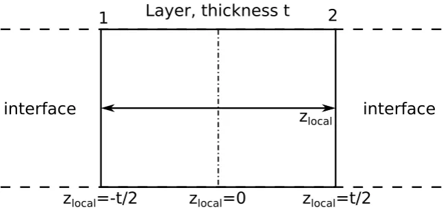
Layer, thickness t
zlocal=0 zlocal=t/2
zlocal=-t/2
zlocal
1 2
[image:18.595.138.462.75.233.2]interface interface
Figure 3.1: Definition of a local coordinate system for a layer.
3.4
Calculate integration constants
After the BVs are calculated, the solver performs the fourth and last step. This step consists of calculating the integration constants from the BVs and with that obtaining the full spatial solution of the system. As can be seen in 2.9, the general solutions to the system contain three integration constants. The first of these is
K1(n). Before calculating K1(n), we first define local coordinate systems for the layers like in figure 3.1.
Now that we have our system of reference, we continue by deriving K1(n,2),3 such that the local solutions in the layer match with the earlier obtained BVs. Since
K1(n) is the only unknown in µ(n)(z) (2.9a), simply substituting z = −tn 2 and
µ(n)(−tn 2 ) =µ
(n)
1 (i.e. the BV on the left side of the layer) gives us an expression
which can be solved easily for K1(n):
K1(n)=µ(1n)+1
2αntJ−βn∆µ
(n)
1 . (3.9)
Calculating K2(n) and K3(n) is slightly more complicated, since they both appear in the expression for ∆µ(n)(z) (2.9b). Two unknowns means we need two expressions:
one is obtained by substituting z = −tn
2 and ∆µ
(n)(−tn
2) = ∆µ (n)
1 and one by
substituting z = +tn
2 and ∆µ
(n)(+tn
2) = ∆µ (n)
2 into 2.9b. Solving this system of
equations yields the expressions forK2(n) and K3(n):
K2(n) = 1 sinhδn
h
∆µ(2n)eδn/2−∆µ(n) 1 e
−δn/2i,
K3(n) = 1 sinhδn
h
∆µ(1n)eδn/2−∆µ(n) 2 e
−δn/2i.
(3.10a)
(3.10b)
Now we can simply substitute these integration constants into 2.9 to obtain the final solutions for µ,∆µ and ∆J inside the layers.
3.5
Precision
One major issue that occurred with this transfer matrix method has to do with the precision at which the floating points are handled. When the solver steps, described in the sections above, were implemented correctly, the results showed incorrect behavior for a lot of system setups, mainly ones with relatively thick layers, or ones with a relatively high number of layers.
As can be seen in 3.11, the element WVF
layer,14 consists of two parts: one linear in
δ and one hyperbolic in δ, i.e. WVFlayer,14 = A·δ+Bsinhδ. Upon investigation, it turned out that the failure of the solver occurred when the relative difference between these linear and hyperbolic terms became of 19 orders of magnitude, i.e. sinhδ/δ ∼1019
WVFlayer =
1 β(coshδ−1) βrsinhδ (1−β2)r
sfδ+β2rsfsinhδ
0 coshδ rsfsinhδ βrsfsinhδ
0 r1
sf sinhδ coshδ β(coshδ−1)
0 0 0 1
. (3.11)
At this point, a 80-bit container with a 63-bit mantissa 1 was used to store floating
point variables. Calculating the precision of the datatype yields:
263 = 9.223372036854776·1018 ≈1019 (3.12)
or a precision of 19 orders of magnitude. This coincidence led to the hypothesis, that the loss of the linear term in WVF
layer,14 due to a lack of precision led to the
failure of the solver.
In order to increase the precision and thereby solve this issue, an arbitrary precision container for floats, following the IEEE 754-2008 standard, was implemented. This container allows all bitwidths which are a multiple of 32.
After implementing this arbitrary precision model and increasing the bitwidth, the output of the solver turned out to be physically correct (see chapter 4). All the results in chapter 4 were obtained using a bitwidth of 1856.
1The mantissa is the part of the container used to store the actual number. The rest is used
Chapter 4
Results
Now that it is clear what the solver calculates and with which methods, we can take a look at the results the solver produces. What the solver basically does is it calculates µ,∆µand ∆J for the given system, returns these calculated values and, if asked for, produces plots of these values throughout the system.
4.1
Identity Interface Model
4.1.1
NFN
First, the solver was tested on different systems using the identity matrix for all the interface transfer matrices. One of these systems is an NFN geometry (a ferromagnetic layer, sandwiched between two nonmagnetic layers) and its solutions can be seen in figure 4.1. Please note that a vector notation was used here to denote layer numbers (i.e. β = (β1, β2, β3)). Also,ρ∗ andlsf in the leads need to be
known for the calculation ofrsf in the leads (3.5c and 3.6c). They are defined to be
equal toρ∗ and lsf in the adjacent N layers. The layers are separated by vertical,
dotted lines. The solid lines represent the solution curves, the triangles the BVs.
0 2 4 6 8 10 12 14 z
0 2 4 6 8 10 12
µ
µ
vs. z
(a) µ
0 2 4 6 8 10 12 14 z
0.4 0.2 0.0 0.2 0.4
∆
µ
∆µ
vs. z
(b) ∆µ
0 2 4 6 8 10 12 14
z 0.8
0.6 0.4 0.2 0.0
∆
J
[image:21.595.99.501.601.716.2](c) ∆J
Figure 4.1: Solver results for an NFN geometry witht= (5,5,5),
Looking at figure 4.1, we see first of all that the solution curves match the BVs at the boundaries and thatµ(z = 0) = 0, as defined in 3.4. It can also be seen, that the derivative of the chemical potential is always positive. This is correct, since
µis proportional to V, with proportionality constant e <0, and the voltage in a passive system in steady state never spontaneously rises. Also note the fact that the curve forµis a straight line in the N layers, which is correct since J andρ∗ are constant within the layers. Further note the lack of discontinuities at the interfaces, which should be the case when using the identity interface model.
Furthermore, we can see that our system is symmetric around the center of the F layer (zlocal = 0). We take this point as the origin of our global frame of reference.
If we now do a thought experiment in which we reverse the direction of the total current density (i.e. Jnew = −Jold), we can imagine that the behaviour of the
system would remain exactly the same (since the system is symmetric), except for the reversed current direction. Mathematically, this means we can write the spin-dependent chemical potential and current density as functions of the global position z and J:
µ±(z, J) = µ±(−z,−J), (4.1a)
J±(z, J) = −J±(−z,−J). (4.1b)
If we now imagine sending in both the positive and the negative current, the total current density would become zero and the solutions for µ± and J± would be superpositions of the solutions for both currents. Since the total current would become zero, the solutions for µ+(z) and µ−(z) would be equal and constant:
µ±(z, J) +µ±(z,−J) = const.≡α, (4.2a)
⇒ µ±(z, J) = α−µ±(−z, J), (4.2b)
withα= 2·µ±(0, J)⇒µ+(0) =µ−(0). (4.2c)
J±(z, J) +J±(z,−J) = J±(z, J)−J±(−z, J) = 0, (4.2d)
⇒J(z, J) =J(−z, J). (4.2e)
With this, we can now prove the symmetries in µ,∆µ and ∆J, using the same, constant J throughout the derivation:
µ(z)≡ 1
2
µ(z)++µ(z)− (4.3a)
⇒µ(−z) = 1 2
µ(−z)++µ(−z)−= 1 2
α+α−µ(z)+−µ(z)− (4.3b)
⇒µ(−z) = 2µ(0)−µ(z) ⇒ antisymmetric with an offset. (4.3c)
∆µ(z)≡ 1
2
µ(z)+−µ(z)− (4.3d)
⇒∆µ(−z) = 1 2
µ(−z)+−µ(−z)−= 1 2
α−α−µ(z)++µ(z)− (4.3e)
⇒∆µ(−z) = −∆µ(z)⇒ ⇒antisymmetric. (4.3f)
∆J(z)≡J(z)+−J(z)− (4.3g)
⇒∆J(−z) = J(−z)+−J(−z)− =J(z)+−J(z)− (4.3h)
⇒∆J(−z) = ∆J(z) ⇒ symmetric. (4.3i)
A similar derivation can be used to show that in an antisymmetrical geometry, µ(z) should be antisymmetric with an offset, ∆µ(z) symmetric and ∆J(z) antisymmetric. As can be seen in figures 4.1 and 4.2, the predicted symmetries are present in the solver result.
Lastly, note that both ∆µ and ∆J have an exponential form in the nonmagnetic layers and go to zero as we go away from the F-N interface. This is correct since the N layers have the same properties (ρ∗, lsf, β) as the leads, and inside the leads
any deviations from equilibrium should decay exponentially, since the system is governed by a spin-diffusion type equation (2.5).
4.1.2
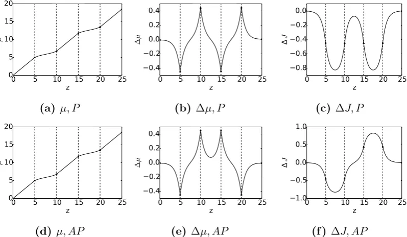
Spin Valves
In addition to the NFN system, the solver was also tested on the parallel (P) and antiparallel (AP) spin valves, which are NFNFN geometries where the magnetiza-tions in the F layers point respectively in equal and opposite direcmagnetiza-tions.
The results of these spin valves can be seen in figure 4.2. Here it can be seen that all the signs of correctness that were checked with the NFN geometry also hold for the two spin valves. Note that for the AP spin valve the magnetization is antisymmetric in z around the center of the geometry, whereas for the P spin valve it is symmetric. This can be seen in figure 4.2 by the fact that ∆µ has an antisymmetric solution and ∆J a symmetric one in the P case, while ∆µ has a symmetric solution and ∆J an antisymmetric one in the AP case.
0 5 10 15 20 25 z 0 5 10 15 20 µ
µ
vs. z
(a) µ, P
0 5 10 15 20 25
z 0.4 0.2 0.0 0.2 0.4 ∆ µ
∆µ
vs. z
(b) ∆µ, P
0 5 10 15 20 25 z 0.8 0.6 0.4 0.2 0.0 ∆ J
(c) ∆J, P
0 5 10 15 20 25
z 0 5 10 15 20 µ
µ
vs. z
(d) µ, AP
0 5 10 15 20 25
z 0.4 0.2 0.0 0.2 0.4 ∆ µ
∆µ
vs. z
(e) ∆µ, AP
0 5 10 15 20 25
z 1.0 0.5 0.0 0.5 1.0 ∆ J
[image:24.595.101.500.81.313.2](f ) ∆J, AP
Figure 4.2: Solver results for the P and AP spin valve geometries with
t= (5,5,5,5,5), β±= (0,0.9,0,±0.9,0), ρ∗ = (1,1,1,1,1), lsf = (1,1,1,1,1)
and J = 1.
0 1 2 3 4 5
z 01 2 3 4 5 µ
µ
vs. z; black=P, red=AP
(a) µ
0 1 2 3 4 5
z 0.4 0.30.2 0.1 0.0 0.1 0.2 0.3 0.4 ∆ µ
∆µ
vs. z; black=P, red=AP
(b) ∆µ
0 1 2 3 4 5
z 0.4 0.30.2 0.1 0.0 0.1 0.2 0.3 ∆ J
(c) ∆J
Figure 4.3: Solver results for the P and AP spin valve geometries to show
the effect of GMR. t= (1,1,1,1,1), β± = (0,0.9,0,±0.9,0), ρ∗ = (1,1,1,1,1),
lsf = (1,1,1,1,1) andJ = 1.
4.2
Non-identity Interface Models
After this, the solver was tested on the NFN geometry, using different interface models. All the following results, including this section and the next one, are ob-tained using the following parameters: t=(1,1,1),β = (0,0.9,0), ρ∗ = (1,1,1,1,1),
lsf = (1,1,1,1,1) and J = 1.
The first interface model is the Valet-Fert (VF) interface model and the results can be seen in figure 4.4. These results show the same signs of correctness as in figure 4.1: µ(0) = 0,∂µ∂z >0, curves that match the BVs, ∆µ(±∞) = 0,∆J(±∞) = 0, similar forms and (anti)symmetry. However, this time there is a step in µ and ∆µ at the interfaces. On the contrary, ∆J is still continuous, albeit non-smooth.
Looking back at figure 2.2, we see that these results are in line with the theory,
[image:24.595.111.501.390.496.2]since in a series circuit the voltage can drop but the current will be conserved. The fact that there is a step in ∆µ, even though RA=RB, can be explained with the fact that the incident ∆J is not zero, as can be seen in figure 4.4c. Since
µ2±−µ±1 =R·J1±,2, the drops in µ+ and µ− are not equal and thus there is a step in ∆µat the interface.
0 2 4 6 8 10 12 14 z 0 2 4 6 8 10 12 14 16 18 µ
µ
vs. z
(a) µ
0 2 4 6 8 10 12 14 z 0.8 0.6 0.40.2 0.0 0.2 0.4 0.6 0.8 ∆ µ
∆µ
vs. z
(b) ∆µ
0 2 4 6 8 10 12 14 z 0.8 0.7 0.6 0.5 0.4 0.3 0.2 0.1 0.0 ∆ J
[image:25.595.96.501.406.522.2](c) ∆J
Figure 4.4: Solver results for the NFN geometries. im=VF,RA= 5, RB = 5.
The results for the Bass-Pratt (BP) and 6 resistance (R6) interface models can be found respectively in figures 4.5 and 4.6. Again, the same signs of correctness can be seen as in the previous figures. Apart from that, we can see that this time there are steps at the interfaces in all the variables.
0 2 4 6 8 10 12 14 z 0 2 4 6 8 10 12 14 16 µ
µ
vs. z
(a) µ
0 2 4 6 8 10 12 14 z 0.8 0.6 0.40.2 0.0 0.2 0.4 0.6 0.8 ∆ µ
∆µ
vs. z
(b) ∆µ
0 2 4 6 8 10 12 14 z 0.9 0.8 0.7 0.6 0.5 0.4 0.30.2 0.1 0.0 ∆ J
(c) ∆J
Figure 4.5: Solver results for the NFN geometries. im=BP,γ = 0.9, δint= 1,
rint = 5.
0 2 4 6 8 10 12 14 z 0 2 4 6 8 10 12 14 µ
µ
vs. z
(a) µ
0 2 4 6 8 10 12 14 z 0.4 0.2 0.0 0.2 0.4 ∆ µ
∆µ
vs. z
(b) ∆µ
0 2 4 6 8 10 12 14
z 1.0 0.8 0.6 0.4 0.2 0.0 0.2 0.4 ∆ J
(c) ∆J
Figure 4.6: Solver results for the NFN geometries. im=R6,
[image:25.595.103.504.580.726.2]4.3
Interface Parameter Dependent Step Sizes
So when using a non-identity interface model, we get steps in µ,∆µ,∆J at the interfaces. This fact, however, is not a very interesting result. What is more inter-esting is how those interface step sizes depend on the interface model parameters. In order to study these dependencies, we define ∆µavg. and ∆µstep according to 4.4.
∆µ4 ≡∆µavg.+ ∆µstep, (4.4a)
∆µ3 ≡∆µavg.−∆µstep. (4.4b)
We conduct similar definitions for µavg., µstep, ∆Javg. and ∆Jstep. The values for
the NF interface, containing the 3rd and 4th BVs (see figure 2.1), were used.
4.3.1
Valet-Fert
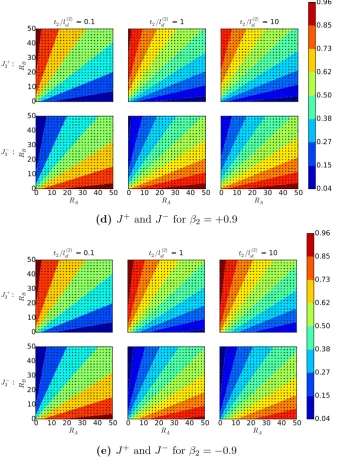
The parameter space of the Valet-Fert interface model (VFIM) spans only two dimensions: RA and RB. However, since we are also interested in the effects of spin accumulation, the layer thickness over the spin-diffusion length of the F layer (i.e. t2/l
(2)
sf ) was added as a third dimension. In plot sheets, we are able to visualize
four dimensions: two on the plots axes and two on the plot grid on the sheet. The fourth and last dimension was used to portray either the values for both spins or the values for both the step and the average in the same plot (see figure 4.7).
Looking at figure 4.7a, that µstep goes to zero as RA and RB go to zero. This is correct, since two parallel, resistanceless channels let the incoming signal pass through unchanged. Also note that as RA and RB increase, µstep and µavg. seem to evolve as [R−A1+R−B1]−1. This is correct, since that is the formula for the total
resistance of two parallel resistances.
Looking at figure 4.7b, we see that ∆µstep increases asRA increases. This seems correct, since ifRA increases we expect (µ+4 −µ
+
4) to increases, meaning that ∆µstep
increases. The opposite holds for RB and ∆µstep. Also note that when RA and RB are equal, ∆µstep does not become zero. This is due to the fact that the spin-up
current encounters more resistance in the F layer than the spin-down current (i.e.
ρ↑ < ρ↓), meaning that J+ 6=J− whenRA=RB, causing a difference in the two spin-dependent chemical potential steps.
Furthermore, when we compare 4.7b to 4.7c, we see that
∆µstep(β2 = 0.9)>∆µstep(β2 =−0.9). This effect seems logical if we think of
the NF interface and the F layer as two parallel series circuits, neglecting spin-flipping (which is a relatively small effect anyways). If β2 = 0.9 ⇒ ρ↑ < ρ↓ in the F layer, causing (µ+4 −µ+4) to increase and (µ+3 − µ+3) to decrease and thus ∆µstep(β2 = 0.9) to increase. Since the opposite is true for β2 = −0.9,
∆µstep(β2 = 0.9)>∆µstep(β2 =−0.9) seems correct.
0 10 20 30 40 50 RB
t2/lsf(2) = 0.1 t2/lsf(2) = 1 t2/lsf(2) = 10
0 10 20 30 40 50
RA 0 10 20 30 40 50 RB
0 10 20 30 40 50
RA
0 10 20 30 40 50
RA 0.00 2.19 4.38 6.56 8.75 10.94 13.12 15.31 17.50
µavg.:
µstep:
(a) µstep and µavg. forβ2 = +0.9
0 10 20 30 40 50 RB
t2/lsf(2) = 0.1 t2/lsf(2) = 1 t2/lsf(2) = 10
0 10 20 30 40 50
RA 0 10 20 30 40 50 RB
0 10 20 30 40 50
RA
0 10 20 30 40 50
RA -1.25 -1.03 -0.82 -0.60 -0.39 -0.17 0.04 0.26 0.47
∆µavg.:
∆µstep:
(b) ∆µstep and ∆µavg. forβ2 = +0.9
0 10 20 30 40 50 RB
t2/lsf(2) = 0.1 t2/lsf(2) = 1 t2/lsf(2) = 10
0 10 20 30 40 50
RA 0 10 20 30 40 50 RB
0 10 20 30 40 50
RA
0 10 20 30 40 50
RA -0.47 -0.26 -0.04 0.17 0.39 0.60 0.82 1.03 1.25
∆µavg.:
∆µstep:
0 10 20 30 40 50
RB
t2/lsf(2) = 0.1 t2/lsf(2) = 1 t2/lsf(2) = 10
0 10 20 30 40 50
RA
0 10 20 30 40 50
RB
0 10 20 30 40 50
RA
0 10 20 30 40 50
RA
0.04 0.15 0.27 0.38 0.50 0.62 0.73 0.85 0.96
J+
3 :
J−
3 :
(d) J+ and J− forβ2= +0.9
0 10 20 30 40 50
RB
t2/lsf(2) = 0.1 t2/lsf(2) = 1 t2/lsf(2) = 10
0 10 20 30 40 50
RA
0 10 20 30 40 50
RB
0 10 20 30 40 50
RA
0 10 20 30 40 50
RA
0.04 0.15 0.27 0.38 0.50 0.62 0.73 0.85 0.96
J+
3 :
J−
3 :
(e) J+ and J− forβ
[image:28.595.130.468.159.626.2]2=−0.9
Figure 4.7: Step sizes in and average interface values of µ,∆µ and J+, J−
plotted vs. RA, RB and t2/l(2)sf for β2 ∈ (−0.9,0.9) for the VFIM. Every dot
represents the result of one simulation.
01 2 3 4
δint
, γ = − 0 . 9
t2/lsf(2) = 0.1 t2/lsf(2) = 1 t2/lsf(2) = 10
01 2 3 4
δint
, γ = − 0 . 45 01 2 3 4
δint
, γ = 0 01 2 3 4
δint
, γ = 0 . 45
1 2 3 4
rint
01 2 3 4
δint
, γ = 0 . 9
1 2 3 4
rint 1 2 3 4rint
6.00 7.29 8.59 9.88 11.17 12.47 13.76 15.06 16.35
(a) µavg.
01 2 3 4
δint
, γ = − 0 . 9
t2/lsf(2) = 0.1 t2/lsf(2) = 1 t2/lsf(2) = 10
01 2 3 4
δint
, γ = − 0 . 45 01 2 3 4
δint
, γ = 0 01 2 3 4
δint
, γ = 0 . 45
1 2 3 4
rint
01 2 3 4
δint
, γ = 0 . 9
1 2 3 4
rint 1 2 3 4rint
0.00 1.29 2.59 3.88 5.17 6.47 7.76 9.06 10.35
[image:29.595.94.501.74.387.2](b) µstep
Figure 4.8: Step sizes in and average interface values of µplotted vs. γ, r, δ
and t2/l(2)sf for β2 = 0.9 for the BPIM. Every dot represents the result of one
simulation.
If we look at figures 4.7d and 4.7e, we see that an increase in RA leads to an decrease in J+ and an increase in J− and that the opposite hold for an increase in RB. This is correct, since the current drops as the resistance increases and
J =J++J− = const.
Finally, increasing t2/l (2)
sf basically represses the effects caused by the difference
in ρ↑ and ρ↓. This can be seen in figures 4.7d and 4.7e, where for β2 = 0.9, J+
decreases and J− increases, while ρ↑ < ρ↓. For β2 = −0.9, J+ increases and J−
decreases, while ρ↓ < ρ↑.
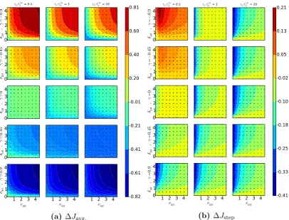
4.3.2
Bass-Pratt
The parameter space of the Bass-Pratt interface model (BPIM) spans three dimen-sions: γ, rint and δint, equivalent to β, rsf and δ for the VF layer transfer matrix.
Since we are again also interested in the effects of spin accumulation, the layer thickness over the spin-diffusion length of the F layer (i.e. t2/l
(2)
sf ) was added as a
01 2 3 4
δint
, γ = − 0 . 9
t2/lsf(2) = 0.1 t2/lsf(2) = 1 t2/lsf(2) = 10
01 2 3 4
δint
, γ = − 0 . 45 01 2 3 4
δint
, γ = 0 01 2 3 4
δint
, γ = 0 . 45
1 2 3 4
rint
01 2 3 4
δint
, γ = 0 . 9
1 2 3 4
rint 1 2 3 4rint
-0.82 -0.61 -0.41 -0.21 -0.01 0.20 0.40 0.60 0.81
(a) ∆Javg.
0 1 2 3 4
δint
, γ = − 0 . 9
t2/lsf(2) = 0.1 t2/lsf(2) = 1 t2/lsf(2) = 10
0 1 2 3 4
δint
, γ = − 0 . 45 0 1 2 3 4
δint
, γ = 0 0 1 2 3 4
δint
, γ = 0 . 45
1 2 3 4
rint 0 1 2 3 4
δint
, γ = 0 . 9
1 2 3 4
rint 1 2 3 4rint
-0.41 -0.33 -0.25 -0.18 -0.10 -0.02 0.05 0.13 0.21
[image:30.595.96.503.232.541.2](b) ∆Jstep
Figure 4.9: Step sizes in and average interface values of ∆J plotted vs. γ, r, δ
and t2/l(2)sf for β2 = 0.9 for the BPIM. Every dot represents the result of one
simulation.
2 46 8 RB , D = 0
C = 0 C = 0.05
E=0,F=0
C = 0.1
2 46 8 RB , D = 0 . 05 E=0,F=0
2 4 6 8
RA 2 46 8 RB , D = 0 . 1
2 4 6 8
RA
2 4 6 8
RA E=0,F=0 0.13 0.21 0.28 0.36 0.43 0.51 0.58 0.66 0.73
(a) J4+
2 46 8 RB , D = 0
C = 0 C = 0.05
E=0,F=0
C = 0.1
2 46 8 RB , D = 0 . 05 E=0,F=0
2 4 6 8
RA 2 46 8 RB , D = 0 . 1
2 4 6 8
RA
2 4 6 8
RA E=0,F=0 0.27 0.34 0.42 0.49 0.57 0.64 0.72 0.79 0.87
[image:31.595.89.504.74.300.2](b) J4−
Figure 4.10: J4+ andJ4− plotted vs. RA, RB, C, Dfort2/lsf(2)= 1, β2 = 0.9 and
E, F = 0 for the R6IM. Every dot represents the result of one simulation.
expected since the virtual layer resistance r=rsfδ(1−γ2). Also since the BPIM
uses a virtual layer to describe an interface one would expect to see some coupling betweenγ and β2, just the coupling that the principle of GMR is based upon. As
can be seen in the plots by comparing the result for γ = 0.9 and γ = −0.9 or
γ = 0.45 and γ =−0.45, whenγ is positive (i.e. aligned with β2) the step in µis
slightly smaller, but the effect is very minimal.
By looking at the figure, we can see that the plots confirm that WBPint is equal to the identity matrix for δint = 0, which is correct, since a layer with thickness
zero can not have any effects. We could continue this kind of explanation for all the effects of the BPIM and pointing out that they are indeed equivalent to the effects an actual F or N layer. However, the most important point to notice when examining the BPIM is that its behaviour is more complicated (see figures 4.9a and 4.9b) and less directly correlated to its parameters in comparison to the VFIM and (as will become clear in the next subsection) the 6 resistances model.
4.3.3
6 Resistances
The parameter space of the 6 resistances interface model (R6IM) spans six dimen-sions: A,B,C,D,E and F. Since the reciprocals of A and B (A−1 =R
2 46 8 RB , D = 0
C = 0 C = 0.05
E=0.05,F=0.05
C = 0.1
2 46 8 RB , D = 0 . 05 E=0.05,F=0.05
2 4 6 8
RA 2 46 8 RB , D = 0 . 1
2 4 6 8
RA
2 4 6 8
RA E=0.05,F=0.05 -0.25 -0.08 0.09 0.25 0.42 0.59 0.76 0.93 1.10
(a) J4+
2 46 8 RB , D = 0
C = 0 C = 0.05
E=0.05,F=0.05
C = 0.1
2 46 8 RB , D = 0 . 05 E=0.05,F=0.05
2 4 6 8
RA 2 46 8 RB , D = 0 . 1
2 4 6 8
RA
2 4 6 8
RA E=0.05,F=0.05 -0.10 0.07 0.24 0.41 0.58 0.75 0.91 1.08 1.25
[image:32.595.89.505.72.302.2](b) J4−
Figure 4.11: J4+ andJ4− plotted vs. RA, RB, C, Dfort2/lsf(2)= 1, β2 = 0.9 and
E, F = 0.05 for the R6IM. Every dot represents the result of one simulation.
Furthermore, by looking at the figure, we see thatJ4+ increases andJ4−decreases as we increase C. This inverse is the case as we increases D. This is in agreement with the expected behaviour from the electrical circuit (see figure 2.3). However, we can also see in the figure that J4+ and J4− show similar behaviour when we increase both C and as when C,D=0, but mirrored around the lineRA=RB. Why this is, is not entirely clear.
Finally, by comparing figures 4.11a and 4.11b to 4.10a and 4.10b we see that increases E and F decreases the differences between the two spin currents. This is correct, since increasing the conductivity of E and F, both the spin accumulation on the left side (i.e. the difference between µ+3 and µ−3) and on the right side (i.e. the difference between µ+4 andµ−4) of the interface are allowed to relax out more. When we also increase C, it can be seen in the figure that J4+ and J4− become less dependent onRA. The same is the case for increased D and less dependence on
RB.
Chapter 5
Conclusions
First of all, we can conclude that the solver created for this report allows for the correct calculation of spin transport through magnetic multilayers according to the theory from the VF paper, when using the identity interface model. The other interface models seem to be implemented correctly as well, since the results seem to behave as expected.
As for the behaviour of the the three interface models, the Valet-Fert interface model proved to be a simple and relatively easy to understand interface model. However, as was known beforehand, it is not able to model spin-flipping at the interfaces.
The Bass-Pratt interface model is able to model more complicated behaviour. Also, since it behaves just as a (ferro)magnetic layer, we can simply apply all acquired knowledge of the VF theory of spin transport to predict the behaviour of this interface model. However, since it models more complicated behaviour with only three parameters, its behaviour seems to be less directly correlated to its parameters, which might make it harder to match the interface model to actual (theoretically of experimentally determined) behaviour at an interface.
Chapter 6
Future Recommendations
First of all, the solver created for this report is still in a very user-unfriendly state. Some pieces of interface codes were written in order to be able to call the solver back-end more easily, to be able to change the solver input without having to write them into the solver code itself and to be able to comfortably perform parameter sweeps with the solver to create plot sheets like the one in figure 4.7. However, most tasks still require the user to edit the back-end, which is not practical for anyone who has not written the code itself.
Therefore, the first recommendation would be to improve the interface codes to the point were one could use the solver without ever having to touch the back-end.
Furthermore, all the plot sheets that can be seen in this report were created using simulations on NFN geometries. In order to gain a deeper understanding of the behaviour of the interface models, plot sheets would have to be created and analyzed using different geometries (e.g. spin valves).
References
[1] T. Valet and A. Fert, PRB 48 (1993) 7099
[2] R.J.H. Wesselink, PhD. thesis, unpublished