Structure Analysis of GaN Thin Film with Inversion Domains by High Voltage Atomic Resolution Microscopy
5
0
0
Full text
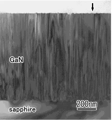
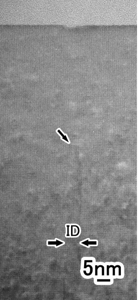
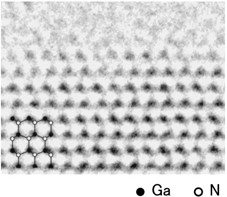
(2) Structure Analysis of GaN Thin Film with Inversion Domains by High Voltage Atomic Resolution Microscopy. 1543. 3. Results 3.1 Atomic resolution observation of GaN film First of all, an imaging condition of GaN was studied by HVARM. Figure 1 is a typical high-resolution image of GaN taken by HVARM. In order to compare to the experimental image, multislice and image simulations were performed using electron microscopy software developed by Ishizuka and Uyeda.21) The calculated image at Scherzer defocus and 3.2 nm in thickness and a schematic atomic structure model are inserted in the figure. The insertions suggest that Ga atomic columns are imaged as strong dark spots and N atomic columns are imaged as weak dark spots under these conditions. Experimental image in Fig. 1 is taken under almost the same defocus and thickness conditions as the calculation. In the experiment, focus series around the Scherzer condition were taken, and the thickness of the sample were checked by comparing the experimental image variation and the calculated image variation depending on the amount of the defocus. The experimental image is in good agreement with the calculated image and reveals that the discrimination between Ga and N is possible. Therefore, in this paper, absolute polarity of GaN was determined by the image taken under these conditions. 3.2 Atomic structure of the GaN film grown on a nitrided sapphire Figure 2 is the bright field image of the GaN film grown on a nitridation sapphire. The polarity of the film assumed to be mainly N-polarity by CAICISS.5) In Fig. 2, high density of domains crosses over the GaN film. The surface also contains high density of pyramids that are about 7 nm in height and 7–15 nm in width. An arrow denotes one of the pyramids at the surface. Figure 3 shows a high-resolution image of the GaN surface with pyramids. Arrows denote domain boundaries and “D”s denote the domains. The image suggests that the pyramids are formed at the surface of the nanometric domains. Figure 4 is the enlarged image of one of the domain boudaries in Fig. 3. The absolute polarity can be di-. Fig. 1 High-resolution electron micrograph of GaN taken by HVARM, showing that Ga and N can be resolved in the image. Insets are the simulated image obtained at −35 nm defocus and 3.2 nm thickness and a schematic of the atomic structure model.. Fig. 2 Low magnification image of the GaN film grown on the sapphire substrate. Many pyramids are formed on the surface. An arrow denotes one of the pyramids.. Fig. 3 High-resolution electron micrograph of the GaN surface with pyramids. Arrows denote domain boundaries and “D”s denote the domains. The pyramids are formed at the surface of the nanometric domains.. Fig. 4 High-resolution electron micrograph of the domain boundaries. An arrow denotes a domain boundary and “D” denotes the domain. Insets are the atomic structure models of GaN. The domain with pyramid has Ga-polarity and the rest has N-polarity..
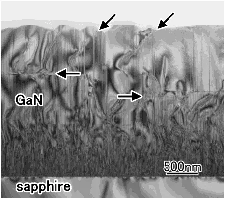
(3) 1544. C. Iwamoto, X.-Q. Shen, H. Okumura, H. Matsuhata and Y. Ikuhara. rectly determined by the ARHVEM image, i.e., the nanometric domain with a pyramid has Ga-polarity and the rest has Npolarity. Thus the domain with the pyramid can be identified to be the inversion domain (ID) and the arrows in Fig. 3 and Fig. 4 are inversion domain boundaries (IDBs). Comparing with the image simulation calculated in Fig. 1, geometrical models for GaN in matrix and the ID are inserted as the insets in Fig. 4. In Fig. 4, Ga and N are distinguishable in most of areas, but in some regions they are indistinguishable due to the weak contrast of the image. However, the distinguishable images enable us to reconstruct the structure of the six membered ring of GaN and determine the absolute polarity even in the weak contrast area. 3.3 Atomic structure of the GaN film with In exposure during film growth Figure 5 is the bright field image of a GaN film with In exposure during film growth. The polarity of the film assumed to be mainly Ga-polarity by CAICISS.5) Many domains are observed in the film and originate at the film/substrate interface. In contrast to the previous observations, density of the domains is reduced at the surface of the film. Although some grooves are observed, the pyramids that were formed at the surface of the nanometric domains are not observed and the surface is almost flat. Defects which directions are parallel or oblique to the film/substrate interface are also observed. In the film, two reduction mechanisms of the density reduction of the domains were observed: domains termination by planar defects and gradual reduction of domains. Figure 6 is the magnified image around the planar defects parallel to the film/substrate interface. The defects, which are denoted by arrows, terminate a lot of domains. Figure 7 is the magnified image at the surface of the film. The domains gradually reduce its diameter from the interface to the surface and several domains disappear inside the film. In this paper, we would like to focus on the mechanism of the gradual reduction of the domains. Figure 8 is the high-resolution image of the domain, which terminates near the surface of the film. At the surface, very large groove, which bottom is almost flat, is. Fig. 6 Magnified image around the planar defects parallel to the film/substrate interface in Fig. 5. Many defects are terminated by the planar defects.. Fig. 7 Magnified image at the surface of the film. Domains gradually reduce its diameter from the interface to the surface and several domains disappear inside the film.. Fig. 8 High-resolution electron micrograph of the domain which terminates near the surface. Fig. 5 Low magnification image of a GaN film with In exposure during film growth. Arrows indicate the defects..
(4) Structure Analysis of GaN Thin Film with Inversion Domains by High Voltage Atomic Resolution Microscopy. 1545. Fig. 10 High-resolution electron micrograph of the domain boundaries. Solid lines denote domain boundaries and “D” denotes the domain. Insets are the atomic structure models of GaN.. Fig. 9 High-resolution electron micrograph of the domain which terminates about 45 nm from the surface.. formed. Figure 9 is the high-resolution image of the domain, which terminates at about 45 nm from the surface. Although small groove is still observed above the domain, the surface is almost flat. Figure 8 and Fig. 9 suggests that domains, which produce the rough surface by making groove at the surface, gradually buried during growth of the film and the surface become flat. Figure 10 is the high-resolution image of the domain boundary, which is denoted by solid lines. The image suggested that the domain has N-polarity and the rest has Gapolarity. Thus the domain is ID like previous observation. In contrast, steps are observed on the IDB. The steps, about one Ga–N atomic pair in height, exist perpendicular to the growth direction. Consequently, the steps are considered to cause the gradual reduction of the ID. 3.4 Atomic structure of the GaN film grown on an AlN high-temperature buffer layer Figure 11 is the bright field image of a GaN film grown on an AlN high-temperature buffer layer. The polarity of the film assumed to be mainly Ga-polarity by CAICISS.5) AlN buffer layer with 200 nm in thickness exists between sapphire and GaN. Around the interface between GaN and AlN or AlN and sapphire, high strain contrast is observed. This configuration is in good agreement with the previous observations.22, 23) In the GaN film, only dislocations are observed and domains, which were observed in Fig. 2 or 5, are hardly observed. The surface of the GaN film is flat. Figure 12 is the high-resolution image of the interface between the AlN buffer layer and the substrate. Near the interface between the film and the substrate, many stacking faults and defects were observed. In addition to the wurtzite-type AlN, zincblend-type AlN was also. Fig. 11 Low magnification image of a GaN film grown on an AlN buffer layer.. Fig. 12 High-resolution electron micrograph of the interface between AlN buffer layer and sapphire substrate..
(5) 1546. C. Iwamoto, X.-Q. Shen, H. Okumura, H. Matsuhata and Y. Ikuhara. 5. Conclusions The morphology and the atomic structure of the GaN films, such as surface and ID morphologies and the polarity of the IDs, were directly determined from only one image taken using HVARM. Three types of the GaN films that have different growth procedure were investigated and the polarity and quality of the film were found to be determined by the density of the IDs. HVARM is thus powerful tool for the investigation of the atomic structure of the GaN films. Acknowledgements A part of this study was financially supported by Grant-inAid for Scientific Research. REFERENCES Fig. 13 High-resolution electron micrograph of GaN film grown on an AlN buffer layer. Inset is the atomic structure model of GaN.. observed. However, domain boundaries, which are observed in previous observations, are hardly observed. Figure 11 and Fig. 12 suggests that the domain did not form from beginning of the deposition. Figure 13 is a high-resolution image of the film near the surface. The polarity of the film is determined to be Ga-polarity. 4. Discussion The present results are directly compared to the previous results. The polarity of the poor-quality GaN film grown by conventional MBE was directly characterized by CAICISS and was assumed to be mainly N-polarity.5) In the present work, HVARM observations of the same sample directly revealed that the poor-quality derived from the high density of Ga-polarity IDs. It was considered that CAICISS gives average information about the lattice-polarity in the film, then, the polarity of nanometric IDs did not significantly contribute to the spectra of the film. On the contrary, the GaN films grown using two different growth procedures were assumed to be Ga-polarity and had a improved quality.5) HVARM observations were in good agreement with these results. In addition, different growth modes were revealed. In the case of GaN with In exposure during the growth, GaN film also had N-polarity IDs. However, the density of IDs was reduced near the surface of the film. In contrast, GaN grown on an AlN buffer had no IDs and was unipolar film. It was considered that the key factor for the improvement in quality was the control of the lattice polarity of the GaN films during the growth.5) Furthermore, HVARM observations of three types of the films indicated that reduction of the density of the N-polarity IDs improve the film quality. Consequently, the control of the density of the IDs during the growth determines the quality and the polarity of the film.. 1) S. Strite and H. Morkoc: J. Vac. Sci. & Technol. B10 (1992) 1237–1266. 2) S. Nakamura, M, Senoh, N. Iwasa, S. Nagahama, T. Yamada and T. Mukai: Jpn. J. Appl. Phys. 34 (1995) L1332–L1335. 3) S. Nakamura, M. Senoh, S. Nagahama, N. Iwasa, T. Yamada, T. Matsushita, Y. Sugimoto and H. Kiyoku: Appl. Phys. Lett. 70 (1997) 2753–2755. 4) E. S. Hellman: MRS Internet J. Nitride Semicond. Res. 3 (1998) 11. 5) X. Q. Shen, T. Ide, S. H. Cho, M. Shimizu, S. Hara, H. Okumura, S. Sonoda and S. Shimizu: Jpn. J. Appl. Phys. 39 (2000) L16–L18. 6) S. Sonoda, S. Shimizu, Y. Suzuki, K. Balakrishnan, J. Shirakashi and H. Okumura: Jpn. J. Appl. Phys. 39 (2000) L73–L75. 7) S. Sonoda, S. Shimizu, X. Q. Shen, S. Hara and H. Okumura: Jpn. J. Appl. Phys. 39 (2000) L202–L204. 8) S. Sonoda, S. Shimizu, K. Balakrishnan and H. Okumura: J. Cryst. Growth. 209 (2000) 364–367. 9) X. Q. Shen, T. Ide, S. H. Cho, M. Shimizu, S. Hara, H. Okumura, S. Sonoda and S. Shimizu: J. Cryst. Growth 218 (2000) 155–160. 10) A. R. Smith, R. M. Feenstra, D. W. Greve, M. S. Shin and M. Showronski: J. Neugebauer and J. E. Northrup: Appl. Phys. Lett. 72 (1998) 2114–2116. 11) X. Q. Shen, T. Ide, S. H. Cho, M. Shimizu, S. Hara, H. Okumura, S. Sonoda and S. Shimizu: Jpn. J. Appl. Phys. 40 (2001) L23–L25. 12) B. Daudin, J. L. Rouviere and M. Arlery: Appl. Phys. Lett. 69 (1997) 2480–2482. 13) L. T. Romano, J. E. Northrup and M. A. O’Keefe: Appl. Phys. Lett. 69 (1996) 2394–2396. 14) F. A. Ponce, D. P. Bour, W. T. Young, M. Saunders and J. W. Steeds: Appl. Phys. Lett. 69 (1996) 337–339. 15) D. Cherns, W. T. Young, M. Saunders, J. W. Steeds, F. A. Ponce and S. Nakamura: Philos. Mag. A 77 (1998) 273–286. 16) V. Potin, P. Ruterana and G. Nouet: J. Appl. Phys. 82 (1997) 2176–2183. 17) V. Potin, P. Ruterana and G. Nouet: Mater. Sci. Eng. B59 (1999) 173– 176. 18) V. Potin, G. Nouet and P. Ruterana: Appl. Phys. Lett. 74 (1999) 947– 949. 19) C. Iwamoto, X. Q. Shen, H. Okumura, H. Matsuhata and Y. Ikuhara: Appl. Phys. Lett. 79 (2001) 3941–3943. 20) H. Ichinose, H. Sawada, E. Takuma and M. Osaki: J. Electon. Microsc. 48 (1999) 887–891. 21) K. Ishizuka and N. Uyeda: Acta Crystallogr., Sect. A: Cryst. Phys., Diffr., Theor. Gen. Crystallogr. 33 (1970) 280–290. 22) K. Hiramatsu, S. Itoh, H. Amano, I. Akasaki, N. Kuwano, T. Shiraishi and K. Oki: J. Cryst. Growth. 115 (1991) 628–633. 23) N. Kuwano, T. Shiraishi, A. Koga, K. Oki, K. Hiramatsu, H. Amano, K. Itoh and I. Akasaki: J. Cryst. Growth. 115 (1991) 381–387..
(6)
Figure
Related documents