MOTOROLA.COM/SEMICONDUCTORS
HCS12
Microcontrollers
"CONTROLLED COPY"
S12MEBIV3/D Rev. 3.00
Multiplexed External
Bus Interface (MEBI)
Block User Guide
Module V3
PRINTED VERSIONS ARE UNCONTROLLED EXCEPT WHEN STAMPED
"CONTROLLED COPY"
IN RED
Block Guide — S12MEBI V3
2
Motorola and the Stylized M Logo are registered trademarks of Motorola, Inc. DigitalDNA is a trademark of Motorola, Inc.
This product incorporates SuperFlash® technology licensed from SST. © Motorola, Inc., 2003
Revision History
Version Number
Revision Date
Effective
Date Author Description of Changes
PRINTED VERSIONS ARE UNCONTROLLED EXCEPT WHEN STAMPED
"CONTROLLED COPY"
IN RED
Table of Contents
Section 1 Introduction
1.1 Overview. . . 6
1.2 Features . . . 6
1.3 Modes of Operation . . . 6
Section 2 External Signal Description
2.1 Overview. . . 92.2 Detailed Signal Descriptions. . . 11
Section 3 Memory Map/Register Definition
3.1 Register Descriptions . . . 143.1.1 Port A Data Register (PORTA) . . . 14
3.1.2 Port B Data Register (PORTB) . . . 15
3.1.3 Data Direction Register A (DDRA) . . . 15
3.1.4 Data Direction Register B (DDRB) . . . 16
3.1.5 Reserved Registers . . . 17
3.1.6 Port E Data Register (PORTE) . . . 17
3.1.7 Data Direction Register E (DDRE) . . . 18
3.1.8 Port E Assignment Register (PEAR) . . . 19
3.1.9 MODE Register (MODE) . . . 21
3.1.10 Pull-Up Control Register (PUCR) . . . 24
3.1.11 Reduced Drive Register (RDRIV) . . . 25
3.1.12 External Bus Interface Control Register (EBICTL) . . . 26
3.1.13 Reserved Register . . . 27
3.1.14 IRQ Control Register (IRQCR) . . . 27
3.1.15 Port K Data Register (PORTK). . . 28
3.1.16 Port K Data Direction Register (DDRK) . . . 29
Section 4 Functional Description
4.1 External Bus Control. . . 314.1.1 Detecting Access Type from External Signals . . . 31
4.1.2 Stretched Bus Cycles. . . 32
4.2 External Data Bus Interface . . . 32
PRINTED VERSIONS ARE UNCONTROLLED EXCEPT WHEN STAMPED
"CONTROLLED COPY"
IN RED
Block Guide — S12MEBI V3
4
4.2.2 Secure Mode . . . 32
4.3 Control . . . 33
4.3.1 Low-Power Options . . . 33
4.3.1.1 Run Mode . . . 33
4.3.1.2 Wait Mode . . . 33
4.3.1.3 Stop Mode . . . 33
4.4 Registers . . . 33
List of Figures
Figure 1-1 MEBI Block Diagram . . . 5Figure 3-1 MEBI Register Map Summary . . . 13
Figure 3-2 Port A Data Register (PORTA) . . . 14
Figure 3-3 Port B Data Register (PORTB) . . . 15
Figure 3-4 Data Direction Register A (DDRA). . . 15
Figure 3-5 Data Direction Register B (DDRB). . . 16
Figure 3-6 Reserved Registers . . . 17
Figure 3-7 Port E Data Register (PORTE) . . . 17
Figure 3-8 Data Direction Register E (DDRE). . . 18
Figure 3-9 Port E Assignment Register (PEAR) . . . 19
Figure 3-10 MODE Register (MODE) . . . 21
Figure 3-11 Pullup Control Register (PUCR) . . . 24
Figure 3-12 Reduced Drive Register (RDRIV) . . . 25
Figure 3-13 External Bus Interface Control Register (EBICTL) . . . 26
Figure 3-14 Reserved Register . . . 27
Figure 3-15 IRQ Control Register (IRQCR) . . . 27
Figure 3-16 Port K Data Register (PORTK) . . . 28
Figure 3-17 Port K Data Direction Register (DDRK) . . . 29
List of Tables
Table 2-1 External System Pins Associated With MEBI . . . 9Table 3-1 MODC, MODB, and MODA Write Capability . . . 22
Table 3-2 Mode Select and State of Mode Bits . . . 23
PRINTED VERSIONS ARE UNCONTROLLED EXCEPT WHEN STAMPED
"CONTROLLED COPY"
IN RED
Section 1 Introduction
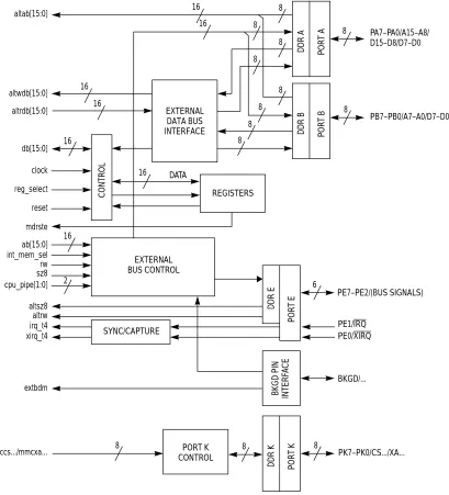
[image:5.612.105.514.209.660.2]This section describes the functionality of the Multiplexed External Bus Interface (MEBI) sub-block of the S12 Core Platform. The functionality of the module is closely coupled with the S12 CPU and the Memory Map Controller (MMC) sub-blocks.
Figure 1-1 is a block diagram of the MEBI. InFigure 1-1, the signals on the right hand side represent pins that are accessible externally. On some chips, these may not all be bonded out.
Figure 1-1 MEBI Block Diagram
CONTR OL REGISTERS POR T K POR T E POR T A DDR K DDR E DDR A POR T B DDR B 8 8 6 8 16 16 16 DATA 8 8 8 8 8 8 8 8 8 16 16 16 16 8 2 PE7–PE2/(BUS SIGNALS) PE1/IRQ PE0/XIRQ BKGD/... PK7–PK0/CS.../XA... mmccs.../mmcxa... extbdm altsz8 altrw irq_t4 xirq_t4 ab[15:0] int_mem_sel rw sz8 cpu_pipe[1:0] mdrste db[15:0] clock reg_select reset altab[15:0] altwdb[15:0] altrdb[15:0] EXTERNAL DATA BUS INTERFACE PA7–PA0/A15–A8/ D15–D8/D7–D0 PB7–PB0/A7–A0/D7–D0 EXTERNAL BUS CONTROL SYNC/CAPTURE PORT K CONTROL
BKGD PIN INTERF
A
C
PRINTED VERSIONS ARE UNCONTROLLED EXCEPT WHEN STAMPED
"CONTROLLED COPY"
IN RED
Block Guide — S12MEBI V3
6
1.1 Overview
The MEBI sub-block of the Core serves to provide access and/or visibility to internal Core data manipulation operations including timing reference information at the external boundary of the Core and/or system. Depending upon the system operating mode and the state of bits within the control registers of the MEBI, the internal 16-bit read and write data operations will be represented in 8-bit or 16-bit accesses externally. Using control information from other blocks within the system, the MEBI will determine the appropriate type of data access to be generated.
1.2 Features
The block name includes these distinctive features:
• External bus controller with four 8-bit Ports A,B, E, and K
• Data and data direction registers for Ports A, B, E, and K when used as general-purpose I/O
• Control register to enable/disable alternate functions on Ports E and K
• Mode control register
• Control register to enable/disable pull-ups on Ports A, B, E, and K
• Control register to enable/disable reduced output drive on Ports A, B, E, and K
• Control register to configure external clock behavior
• Control register to configure IRQ pin operation
• Logic to capture and synchronize external interrupt pin inputs
1.3 Modes of Operation
• Normal Expanded Wide Mode
Ports A and B are configured as a 16-bit multiplexed address and data bus and Port E provides bus control and status signals. This mode allows 16-bit external memory and peripheral devices to be interfaced to the system.
• Normal Expanded Narrow Mode
Ports A and B are configured as a 16-bit address bus and Port A is multiplexed with 8-bit data. Port E provides bus control and status signals. This mode allows 8-bit external memory and peripheral devices to be interfaced to the system.
• Normal Single-Chip Mode
PRINTED VERSIONS ARE UNCONTROLLED EXCEPT WHEN STAMPED
"CONTROLLED COPY"
IN RED
• Special Single-Chip Mode
This mode is generally used for debugging single-chip operation, boot-strapping, or security related operations. The active background mode is in control of CPU execution and BDM firmware is waiting for additional serial commands through the BKGD pin. There is no external expansion bus after reset in this mode.
• Emulation Expanded Wide Mode
Developers use this mode for emulation systems in which the users target application is Normal Expanded Wide Mode.
• Emulation Expanded Narrow Mode
Developers use this mode for emulation systems in which the users target application is Normal Expanded Narrow Mode.
• Special Test Mode
Ports A and B are configured as a 16-bit multiplexed address and data bus and Port E provides bus control and status signals. In special test mode, the write protection of many control bits is lifted so that they can be thoroughly tested without needing to go through reset.
• Special Peripheral Mode
PRINTED VERSIONS ARE UNCONTROLLED EXCEPT WHEN STAMPED "CONTROLLED COPY" IN RED
Block Guide — S12MEBI V3
PRINTED VERSIONS ARE UNCONTROLLED EXCEPT WHEN STAMPED
"CONTROLLED COPY"
IN RED
Section 2 External Signal Description
2.1 Overview
[image:9.612.58.556.235.684.2]In typical implementations, the MEBI sub-block of the Core interfaces directly with external system pins. Some pins may not be bonded out in all implementations.
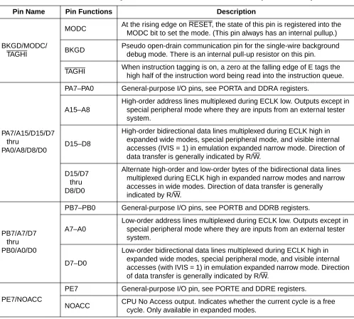
Table 2-1outlines the pin names and functions and gives a brief description of their operation Reset state of these pins and associated pull-ups or pull-downs is dependent on the mode of operation and on the integration of this block at the chip level (chip dependent).
.
Table 2-1 External System Pins Associated With MEBI (Sheet 1 of 3)
Pin Name Pin Functions Description
BKGD/MODC/ TAGHI
MODC At the rising edge on RESET, the state of this pin is registered into the MODC bit to set the mode. (This pin always has an internal pullup.)
BKGD Pseudo open-drain communication pin for the single-wire background debug mode. There is an internal pull-up resistor on this pin.
TAGHI When instruction tagging is on, a zero at the falling edge of E tags the high half of the instruction word being read into the instruction queue.
PA7/A15/D15/D7 thru
PA0/A8/D8/D0
PA7–PA0 General-purpose I/O pins, see PORTA and DDRA registers.
A15–A8
High-order address lines multiplexed during ECLK low. Outputs except in special peripheral mode where they are inputs from an external tester system.
D15–D8
High-order bidirectional data lines multiplexed during ECLK high in expanded wide modes, special peripheral mode, and visible internal accesses (IVIS = 1) in emulation expanded narrow mode. Direction of data transfer is generally indicated by R/W.
D15/D7 thru D8/D0
Alternate high-order and low-order bytes of the bidirectional data lines multiplexed during ECLK high in expanded narrow modes and narrow accesses in wide modes. Direction of data transfer is generally indicated by R/W.
PB7/A7/D7 thru PB0/A0/D0
PB7–PB0 General-purpose I/O pins, see PORTB and DDRB registers.
A7–A0
Low-order address lines multiplexed during ECLK low. Outputs except in special peripheral mode where they are inputs from an external tester system.
D7–D0
Low-order bidirectional data lines multiplexed during ECLK high in expanded wide modes, special peripheral mode, and visible internal accesses (with IVIS = 1) in emulation expanded narrow mode. Direction of data transfer is generally indicated by R/W.
PE7/NOACC
PE7 General-purpose I/O pin, see PORTE and DDRE registers.
PRINTED VERSIONS ARE UNCONTROLLED EXCEPT WHEN STAMPED
"CONTROLLED COPY"
IN RED
Block Guide — S12MEBI V3
10
PE6/IPIPE1/ MODB/CLKTO
MODB At the rising edge of RESET, the state of this pin is registered into the MODB bit to set the mode.
PE6 General-purpose I/O pin, see PORTE and DDRE registers.
IPIPE1 Instruction pipe status bit 1, enabled by PIPOE bit in PEAR.
CLKTO
System Clock Test Output. Only available in special modes. PIPOE = 1 overrides this function. The enable for this function is in the clock module.
PE5/IPIPE0/MO DA
MODA At the rising edge on RESET, the state of this pin is registered into the MODA bit to set the mode.
PE5 General-purpose I/O pin, see PORTE and DDRE registers.
IPIPE0 Instruction pipe status bit 0, enabled by PIPOE bit in PEAR.
PE4/ECLK
PE4 General-purpose I/O pin, see PORTE and DDRE registers.
ECLK
Bus timing reference clock, can operate as a free-running clock at the system clock rate or to produce one low-high clock per visible access, with the high period stretched for slow accesses. ECLK is controlled by the NECLK bit in PEAR, the IVIS bit in MODE, and the ESTR bit in EBICTL.
PE3/LSTRB/ TAGLO
PE3 General-purpose I/O pin, see PORTE and DDRE registers.
LSTRB Low strobe bar, zero indicates valid data on D7–D0.
SZ8 In special peripheral mode, this pin is an input indicating the size of the data transfer (0 = 16-bit; 1 = 8-bit).
TAGLO
In expanded wide mode or emulation narrow modes, when instruction tagging is on and low strobe is enabled, a zero at the falling edge of E tags the low half of the instruction word being read into the instruction queue.
PE2/R/W
PE2 General-purpose I/O pin, see PORTE and DDRE registers.
R/W Read/write, indicates the direction of internal data transfers. This is an output except in special peripheral mode where it is an input.
PE1/IRQ PE1 General-purpose input-only pin, can be read even if IRQ enabled. IRQ Maskable interrupt request, can be level sensitive or edge sensitive.
PE0/XIRQ PE0 General-purpose input-only pin. XIRQ Non-maskable interrupt input.
PK7/ECS PK7 General-purpose I/O pin, see PORTK and DDRK registers. ECS Emulation chip select
[image:10.612.51.553.69.667.2]PK6/XCS PK6 General-purpose I/O pin, see PORTK and DDRK registers. XCS External data chip select
Table 2-1 External System Pins Associated With MEBI (Sheet 2 of 3)
PRINTED VERSIONS ARE UNCONTROLLED EXCEPT WHEN STAMPED
"CONTROLLED COPY"
IN RED
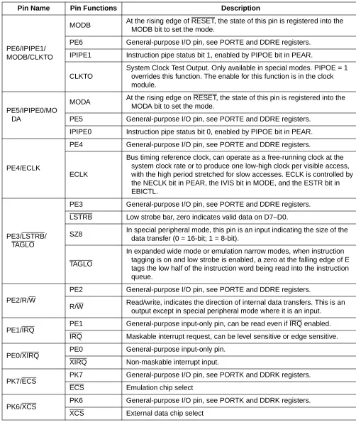
2.2 Detailed Signal Descriptions
Detailed descriptions of these pins can be found in the device specification for the particular chip being used.
PK5/X19 thru PK0/X14
PK5–PK0 General-purpose I/O pins, see PORTK and DDRK registers.
X19–X14 Memory expansion addresses
Table 2-1 External System Pins Associated With MEBI (Sheet 3 of 3)
PRINTED VERSIONS ARE UNCONTROLLED EXCEPT WHEN STAMPED "CONTROLLED COPY" IN RED
Block Guide — S12MEBI V3
PRINTED VERSIONS ARE UNCONTROLLED EXCEPT WHEN STAMPED
"CONTROLLED COPY"
IN RED
Section 3 Memory Map/Register Definition
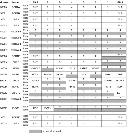
[image:13.612.63.561.152.689.2]A summary of the registers associated with the MEBI sub-block is shown inFigure 3-1. Detailed descriptions of the registers and bits are given in the subsections that follow.On most chips the registers are mappable. Therefore, the upper bits may not be all zeros as shown in the table and descriptions.
Figure 3-1 MEBI Register Map Summary
Address Name Bit 7 6 5 4 3 2 1 Bit 0
$0000 PORTA Read Bit 7 6 5 4 3 2 1 Bit 0
Write
$0001 PORTB Read Bit 7 6 5 4 3 2 1 Bit 0
Write
$0002 DDRA Read Bit 7 6 5 4 3 2 1 Bit 0
Write
$0003 DDRB Read Bit 7 6 5 4 3 2 1 Bit 0
Write
$0004 Reserved Read 0 0 0 0 0 0 0 0
Write
$0005 Reserved Read 0 0 0 0 0 0 0 0
Write
$0006 Reserved Read 0 0 0 0 0 0 0 0
Write
$0007 Reserved Read 0 0 0 0 0 0 0 0
Write
$0008 PORTE Read Bit 7 6 5 4 3 2 1 Bit 0
Write
$0009 DDRE Read Bit 7 6 5 4 3 2 0 0
Write
$000A PEAR Read NOACCE 0 PIPOE NECLK LSTRE RDWE 0 0 Write
$000B MODE Read MODC MODB MODA 0 IVIS 0 EMK EME Write
$000C PUCR Read PUPKE 0 0 PUPEE 0 0 PUPBE PUPAE Write
$000D RDRIV Read RDPK 0 0 RDPE 0 0 RDPB RDPA
Write
$000E EBICTL Read 0 0 0 0 0 0 0 ESTR
Write
$000F Reserved Read 0 0 0 0 0 0 0 0
Write
$001E IRQCR Read IRQE IRQEN 0 0 0 0 0 0
Write
$0032 PORTK Read Bit 7 6 5 4 3 2 1 Bit 0
Write
$0033 DDRK Read Bit 7 6 5 4 3 2 1 Bit 0
Write
PRINTED VERSIONS ARE UNCONTROLLED EXCEPT WHEN STAMPED
"CONTROLLED COPY"
IN RED
Block Guide — S12MEBI V3
14
3.1 Register Descriptions
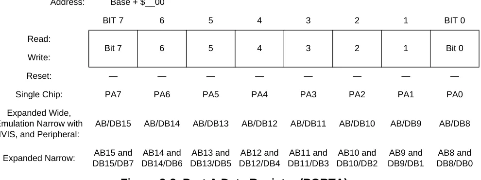
3.1.1 Port A Data Register (PORTA)
Read: anytime when register is in the map
Write: anytime when register is in the map
Port A bits 7 through 0 are associated with address lines A15 through A8 respectively and data lines D15/D7 through D8/D0 respectively. When this port is not used for external addresses such as in single-chip mode, these pins can be used as general-purpose I/O. Data Direction Register A (DDRA) determines the primary direction of each pin. DDRA also determines the source of data for a read of PORTA.
This register is not in the on-chip memory map in expanded and special peripheral modes. Therefore, these accesses will be echoed externally.
NOTE: To ensure that you read the value present on the PORTA pins, always wait at least one cycle after writing to the DDRA register before reading from the PORTA register.
Address: Base + $__00
BIT 7 6 5 4 3 2 1 BIT 0
Read:
Bit 7 6 5 4 3 2 1 Bit 0
Write:
Reset: — — — — — — — —
Single Chip: PA7 PA6 PA5 PA4 PA3 PA2 PA1 PA0
Expanded Wide, Emulation Narrow with
IVIS, and Peripheral:
AB/DB15 AB/DB14 AB/DB13 AB/DB12 AB/DB11 AB/DB10 AB/DB9 AB/DB8
Expanded Narrow: AB15 and DB15/DB7
AB14 and DB14/DB6
AB13 and DB13/DB5
AB12 and DB12/DB4
AB11 and DB11/DB3
AB10 and DB10/DB2
AB9 and DB9/DB1
[image:14.612.65.560.129.314.2]AB8 and DB8/DB0
PRINTED VERSIONS ARE UNCONTROLLED EXCEPT WHEN STAMPED
"CONTROLLED COPY"
IN RED
3.1.2 Port B Data Register (PORTB)
Read: anytime when register is in the map
Write: anytime when register is in the map
Port B bits 7 through 0 are associated with address lines A7 through A0 respectively and data lines D7 through D0 respectively. When this port is not used for external addresses, such as in single-chip mode, these pins can be used as general-purpose I/O. Data Direction Register B (DDRB) determines the primary direction of each pin. DDRB also determines the source of data for a read of PORTB.
This register is not in the on-chip memory map in expanded and special peripheral modes. Therefore, these accesses will be echoed externally.
NOTE: To ensure that you read the value present on the PORTB pins, always wait at least one cycle after writing to the DDRB register before reading from the PORTB register.
3.1.3 Data Direction Register A (DDRA)
Read: anytime when register is in the map
Write: anytime when register is in the map
Address: Base + $__01
BIT 7 6 5 4 3 2 1 BIT 0
Read:
Bit 7 6 5 4 3 2 1 Bit 0
Write:
Reset: — — — — — — — —
Single Chip: PB7 PB6 PB5 PB4 PB3 PB2 PB1 PB0 Expanded Wide,
Emulation Narrow with IVIS, and Peripheral:
AB/DB7 AB/DB6 AB/DB5 AB/DB4 AB/DB3 AB/DB2 AB/DB1 AB/DB0
[image:15.612.81.536.91.267.2]Expanded Narrow: AB7 AB6 AB5 AB4 AB3 AB2 AB1 AB0
Figure 3-3 Port B Data Register (PORTB)
Address: Base + $__02
BIT 7 6 5 4 3 2 1 BIT 0
Read:
Bit 7 6 5 4 3 2 1 Bit 0
Write:
Reset: 0 0 0 0 0 0 0 0
[image:15.612.111.504.545.635.2]PRINTED VERSIONS ARE UNCONTROLLED EXCEPT WHEN STAMPED
"CONTROLLED COPY"
IN RED
Block Guide — S12MEBI V3
16
This register controls the data direction for Port A. When Port A is operating as a general-purpose I/O port, DDRA determines the primary direction for each Port A pin. A “1” causes the associated port pin to be an output and a “0” causes the associated pin to be a high-impedance input. The value in a DDR bit also affects the source of data for reads of the corresponding PORTA register. If the DDR bit is zero (input) the buffered pin input state is read. If the DDR bit is one (output) the associated port data register bit state is read.
This register is not in the on-chip memory map in expanded and special peripheral modes. Therefore, these accesses will be echoed externally. It is reset to $00 so the DDR does not override the three-state control signals.
DDRA7–DDRA0 — Data Direction Port A
1 = Configure the corresponding I/O pin as an output 0 = Configure the corresponding I/O pin as an input
3.1.4 Data Direction Register B (DDRB)
Read: anytime when register is in the map
Write: anytime when register is in the map
This register controls the data direction for Port B. When Port B is operating as a general-purpose I/O port, DDRB determines the primary direction for each Port B pin. A “1” causes the associated port pin to be an output and a “0” causes the associated pin to be a high-impedance input. The value in a DDR bit also affects the source of data for reads of the corresponding PORTB register. If the DDR bit is zero (input) the buffered pin input state is read. If the DDR bit is one (output) the associated port data register bit state is read.
This register is not in the on-chip memory map in expanded and special peripheral modes. Therefore, these accesses will be echoed externally. It is reset to $00 so the DDR does not override the three-state control signals.
DDRB7–DDRB0 — Data Direction Port B
1 = Configure the corresponding I/O pin as an output 0 = Configure the corresponding I/O pin as an input
Address: Base + $__03
BIT 7 6 5 4 3 2 1 BIT 0
Read:
Bit 7 6 5 4 3 2 1 Bit 0
Write:
[image:16.612.109.499.300.392.2]Reset: 0 0 0 0 0 0 0 0
PRINTED VERSIONS ARE UNCONTROLLED EXCEPT WHEN STAMPED
"CONTROLLED COPY"
IN RED
3.1.5 Reserved Registers
These register locations are not used (reserved). All unused registers and bits in this block return logic zeros when read. Writes to these registers have no effect.
These registers are not in the on-chip map in special peripheral mode.
3.1.6 Port E Data Register (PORTE)
Read: anytime when register is in the map
Write: anytime when register is in the map
Port E is associated with external bus control signals and interrupt inputs. These include mode select (MODB/IPIPE1, MODA/IPIPE0), E clock, size (LSTRB/TAGLO), read/write (R/W), IRQ, and XIRQ. When not used for one of these specific functions, Port E pins 7–2 can be used as general-purpose I/O and pins 1–0 can be used as general-purpose input. The Port E Assignment Register (PEAR) selects the function of each pin and DDRE determines whether each pin is an input or output when it is configured to be general-purpose I/O. DDRE also determines the source of data for a read of PORTE.
Some of these pins have software selectable pull-ups (PE7, ECLK, LSTRB, R/W, IRQ, and XIRQ). A single control bit enables the pull-ups for all of these pins when they are configured as inputs
Address: Base + $__04 through $__07
BIT 7 6 5 4 3 2 1 BIT 0
Read: 0 0 0 0 0 0 0 0
Write:
Reset: 0 0 0 0 0 0 0 0
[image:17.612.113.500.91.208.2]= Unimplemented
Figure 3-6 Reserved Registers
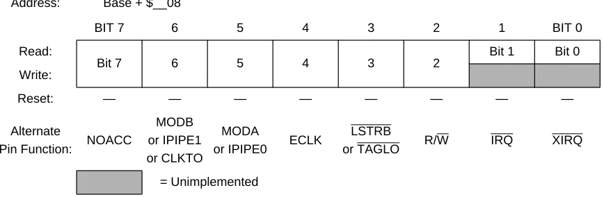
Address: Base + $__08
BIT 7 6 5 4 3 2 1 BIT 0
Read:
Bit 7 6 5 4 3 2
Bit 1 Bit 0 Write:
Reset: — — — — — — — —
Alternate
Pin Function: NOACC
MODB or IPIPE1 or CLKTO
MODA
or IPIPE0 ECLK
LSTRB
or TAGLO R/W IRQ XIRQ
= Unimplemented
[image:17.612.87.521.337.479.2]PRINTED VERSIONS ARE UNCONTROLLED EXCEPT WHEN STAMPED
"CONTROLLED COPY"
IN RED
Block Guide — S12MEBI V3
18
This register is not in the on-chip map in special peripheral mode or in expanded modes when the EME bit is set. Therefore, these accesses will be echoed externally.
NOTE: It is unwise to write PORTE and DDRE as a word access. If you are changing Port E pins from being inputs to outputs, the data may have extra transitions during the write. It is best to initialize PORTE before enabling as outputs.
NOTE: To ensure that you read the value present on the PORTE pins, always wait at least one cycle after writing to the DDRE register before reading from the PORTE register.
3.1.7 Data Direction Register E (DDRE)
Read: anytime when register is in the map
Write: anytime when register is in the map
Data Direction Register E is associated with Port E. For bits in Port E that are configured as
general-purpose I/O lines, DDRE determines the primary direction of each of these pins. A “1” causes the associated bit to be an output and a “0” causes the associated bit to be an input. Port E bit 1 (associated with IRQ) and bit 0 (associated with XIRQ) cannot be configured as outputs. Port E, bits 1 and 0, can be read regardless of whether the alternate interrupt function is enabled. The value in a DDR bit also affects the source of data for reads of the corresponding PORTE register. If the DDR bit is zero (input) the buffered pin input state is read. If the DDR bit is one (output) the associated port data register bit state is read.
This register is not in the on-chip memory map in expanded and special peripheral modes. Therefore, these accesses will be echoed externally. Also, it is not in the map in expanded modes while the EME control bit is set.
DDRE7–DDRE2 — Data Direction Port E
1 = Configure the corresponding I/O pin as an output 0 = Configure the corresponding I/O pin as an input
NOTE: It is unwise to write PORTE and DDRE as a word access. If you are changing Port E pins from inputs to outputs, the data may have extra transitions during the write. It is best to initialize PORTE before enabling as outputs.
Address: Base + $__09
BIT 7 6 5 4 3 2 1 BIT 0
Read:
Bit 7 6 5 4 3 Bit 2
0 0
Write:
Reset: 0 0 0 0 0 0 0 0
[image:18.612.109.502.245.344.2]= Unimplemented
PRINTED VERSIONS ARE UNCONTROLLED EXCEPT WHEN STAMPED
"CONTROLLED COPY"
IN RED
3.1.8 Port E Assignment Register (PEAR)
Read: anytime (provided this register is in the map).
Write: each bit has specific write conditions. Please refer to the descriptions of each bit on the following pages.
Port E serves as general-purpose I/O or as system and bus control signals. The PEAR register is used to choose between the general-purpose I/O function and the alternate control functions. When an alternate control function is selected, the associated DDRE bits are overridden.
The reset condition of this register depends on the mode of operation because bus control signals are needed immediately after reset in some modes. In normal single-chip mode, no external bus control signals are needed so all of Port E is configured for general-purpose I/O. In normal expanded modes, only the E clock is configured for its alternate bus control function and the other bits of Port E are configured for general-purpose I/O. As the reset vector is located in external memory, the E clock is required for this access. R/W is only needed by the system when there are external writable resources. If the normal expanded system needs any other bus control signals, PEAR would need to be written before any access that needed the additional signals. In special test and emulation modes, IPIPE1, IPIPE0, E, LSTRB, and R/W are configured out of reset as bus control signals.
This register is not in the on-chip memory map in expanded and special peripheral modes. Therefore, these accesses will be echoed externally.
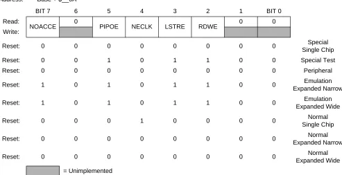
Address: Base + $__0A
BIT 7 6 5 4 3 2 1 BIT 0
Read:
NOACCE 0 PIPOE NECLK LSTRE RDWE 0 0 Write:
Reset: 0 0 0 0 0 0 0 0 Special
Single Chip
Reset: 0 0 1 0 1 1 0 0 Special Test
Reset: 0 0 0 0 0 0 0 0 Peripheral
Reset: 1 0 1 0 1 1 0 0 Emulation
Expanded Narrow
Reset: 1 0 1 0 1 1 0 0 Emulation
Expanded Wide
Reset: 0 0 0 1 0 0 0 0 Normal
Single Chip
Reset: 0 0 0 0 0 0 0 0 Normal
Expanded Narrow
Reset: 0 0 0 0 0 0 0 0 Normal
[image:19.612.60.553.99.352.2]Expanded Wide = Unimplemented
PRINTED VERSIONS ARE UNCONTROLLED EXCEPT WHEN STAMPED
"CONTROLLED COPY"
IN RED
Block Guide — S12MEBI V3
20
NOACCE — CPU No Access Output Enable Normal: write once
Emulation: write never Special: write anytime
1 = The associated pin (Port E, bit 7) is output and indicates whether the cycle is a CPU free cycle. 0 = The associated pin (Port E, bit 7) is general-purpose I/O.
This bit has no effect in single-chip or special peripheral modes.
PIPOE — Pipe Status Signal Output Enable Normal: write once
Emulation: write never Special: write anytime.
1 = The associated pins (Port E, bits 6:5) are outputs and indicate the state of the instruction queue 0 = The associated pins (Port E, bits 6:5) are general-purpose I/O.
This bit has no effect in single-chip or special peripheral modes.
NECLK — No External E Clock Normal and Special: write anytime Emulation: write never
1 = The associated pin (Port E, bit 4) is a general-purpose I/O pin.
0 = The associated pin (Port E, bit 4) is the external E clock pin. External E clock is free-running if ESTR = 0
External E clock is available as an output in all modes.
LSTRE — Low Strobe (LSTRB) Enable Normal: write once
Emulation: write never Special: write anytime.
1 = The associated pin (Port E, bit 3) is configured as the LSTRB bus control output. If BDM tagging is enabled, TAGLO is multiplexed in on the rising edge of ECLK and LSTRB is driven out on the falling edge of ECLK.
0 = The associated pin (Port E, bit 3) is a general-purpose I/O pin.
This bit has no effect in single-chip, peripheral, or normal expanded narrow modes.
PRINTED VERSIONS ARE UNCONTROLLED EXCEPT WHEN STAMPED
"CONTROLLED COPY"
IN RED
RDWE — Read/Write Enable Normal: write once Emulation: write never Special: write anytime
1 = The associated pin (Port E, bit 2) is configured as the R/W pin 0 = The associated pin (Port E, bit 2) is a general-purpose I/O pin. This bit has no effect in single-chip or special peripheral modes.
NOTE: R/W is used for external writes. After reset in normal expanded mode, R/W is disabled to provide an extra I/O pin. If R/W is needed it should be enabled before any external writes.
3.1.9 MODE Register (MODE)
Read: anytime (provided this register is in the map).
Write: each bit has specific write conditions. Please refer to the descriptions of each bit on the following pages.
The MODE register is used to establish the operating mode and other miscellaneous functions (i.e., internal visibility and emulation of Port E and K).
Address: Base + $__0B
BIT 7 6 5 4 3 2 1 BIT 0
Read:
MODC MODB MODA 0
IVIS
0
EMK EME Write:
Reset: 0 0 0 0 0 0 0 0 Special Single Chip
Reset: 0 0 1 0 1 0 1 1 Emulation
Expanded Narrow
Reset: 0 1 0 0 1 0 0 0 Special Test
Reset: 0 1 1 0 1 0 1 1 Emulation
Expanded Wide
Reset: 1 0 0 0 0 0 0 0 Normal Single Chip
Reset: 1 0 1 0 0 0 0 0 Normal
Expanded Narrow
Reset: 1 1 0 0 0 0 0 0 Peripheral
Reset: 1 1 1 0 0 0 0 0 Normal
[image:21.612.72.536.282.550.2]Expanded Wide = Unimplemented
PRINTED VERSIONS ARE UNCONTROLLED EXCEPT WHEN STAMPED
"CONTROLLED COPY"
IN RED
Block Guide — S12MEBI V3
22
In special peripheral mode, this register is not accessible but it is reset as shown to system configuration features. Changes to bits in the MODE register are delayed one cycle after the write.
This register is not in the on-chip memory map in expanded and special peripheral modes. Therefore, these accesses will be echoed externally.
MODC, MODB, and MODA — Mode Select Bits These bits indicate the current operating mode.
If MODA = 1, then MODC, MODB, and MODA are write never.
If MODC= MODA = 0, then MODC, MODB, and MODA are writable with the exception that you cannot change to or from special peripheral mode
[image:22.612.52.562.303.531.2]If MODC = 1, MODB = 0, and MODA = 0, then MODC is write never. MODB and MODA are write once, except that you cannot change to special peripheral mode. From normal single-chip, only normal expanded narrow and normal expanded wide modes are available.
Table 3-1 MODC, MODB, and MODA Write Capability(1)
NOTES:
1. No writes to the MOD bits are allowed while operating in a SECURE mode. For more details, refer to the device user guide.
MODC MODB MODA Mode MODx Write Capability
0 0 0 Special Single Chip MODC, MODB, and MODA
write anytime but not to 110(2)
2. If you are in a special single-chip or special test mode and you write to this register, changing to normal single-chip mode, then one allowed write to this register remains. If you write to normal expanded or emulation mode, then no writes remain.
0 0 1 Emulation Narrow No write
0 1 0 Special Test MODC, MODB, and MODA
write anytime but not to 110(2)
0 1 1 Emulation Wide No write
1 0 0 Normal Single Chip
MODC write never, MODB and MODA write once
but not to 110
1 0 1 Normal Expanded Narrow No write
1 1 0 Special Peripheral No write
PRINTED VERSIONS ARE UNCONTROLLED EXCEPT WHEN STAMPED
"CONTROLLED COPY"
IN RED
IVIS — Internal Visibility (for both read and write accesses)
This bit determines whether internal accesses generate a bus cycle that is visible on the external bus. Normal: write once
Emulation: write never Special: write anytime
1 = Internal bus operations are visible on external bus. 0 = No visibility of internal bus operations on external bus.
EMK — Emulate Port K Normal: write once Emulation: write never Special: write anytime
1 = If in any expanded mode, PORTK and DDRK are removed from the memory map.
0 = PORTK and DDRK are in the memory map so Port K can be used for general-purpose I/O. In single-chip modes, PORTK and DDRK are always in the map regardless of the state of this bit. In special peripheral mode, PORTK and DDRK are never in the map regardless of the state of this bit.
EME — Emulate Port E
Normal and Emulation: write never Special: write anytime
1 = If in any expanded mode or special peripheral mode, PORTE and DDRE are removed from the memory map. Removing the registers from the map allows the user to emulate the function of these registers externally.
[image:23.612.58.560.64.304.2]0 = PORTE and DDRE are in the memory map so Port E can be used for general-purpose I/O. In single-chip modes, PORTE and DDRE are always in the map regardless of the state of this bit.
Table 3-2 Mode Select and State of Mode Bits
Input BKGD and Bit MODC
Input and Bit MODB
Input and Bit MODA
Mode Description
0 0 0
Special Single Chip, BDM allowed and ACTIVE. BDM is “allowed” in all other modes but a serial command is required to make BDM “active”.
0 0 1 Emulation Expanded Narrow, BDM allowed
0 1 0 Special Test (Expanded Wide), BDM allowed
0 1 1 Emulation Expanded Wide, BDM allowed
1 0 0 Normal Single Chip, BDM allowed
1 0 1 Normal Expanded Narrow, BDM allowed
1 1 0
Peripheral, BDM allowed but bus operations would cause bus conflicts
(must not be used)
PRINTED VERSIONS ARE UNCONTROLLED EXCEPT WHEN STAMPED
"CONTROLLED COPY"
IN RED
Block Guide — S12MEBI V3
24
3.1.10 Pull-Up Control Register (PUCR)
Read: anytime (provided this register is in the map).
Write: anytime (provided this register is in the map).
This register is used to select pull resistors for the pins associated with the core ports. Pull resistors are assigned on a per-port basis and apply to any pin in the corresponding port that is currently configured as an input. The polarity of these pull resistors is determined by chip integration. Please refer to the specific device User’s Guide to determine the polarity of these resistors.
This register is not in the on-chip memory map in expanded and special peripheral modes. Therefore, these accesses will be echoed externally.
NOTE: These bits have no effect when the associated pin(s) are outputs. (The pull resistors are inactive.)
PUPKE — Pull-Up Port K Enable
1 = Enable pull resistors for Port K input pins. 0 = Port K pull resistors are disabled.
PUPEE — Pull-Up Port E Enable
1 = Enable pull resistors for Port E input pins bits 7, 4–0. 0 = Port E pull resistors on bits 7, 4–0 are disabled.
NOTE: Bits 5 and 6 of Port E have pull resistors which are only enabled during reset. This bit has no effect on these pins.
PUPBE — Pull-Up Port B Enable
1 = Enable pull resistors for all Port B input pins. 0 = Port B pull resistors are disabled.
PUPAE — Pull-Up Port A Enable
1 = Enable pull resistors for all Port A input pins.
Address: Base + $__0C
BIT 7 6 5 4 3 2 1 BIT 0
Read:
PUPKE
0 0
PUPEE
0 0
PUPBE PUPAE Write:
Reset:(1) 1 0 0 1 0 0 0 0
= Unimplemented
NOTES:
[image:24.612.108.499.99.212.2]1. The default value of this parameter is shown. Please refer to the specific device User’s Guide to determine the actual reset state of this register.
PRINTED VERSIONS ARE UNCONTROLLED EXCEPT WHEN STAMPED
"CONTROLLED COPY"
IN RED
0 = Port A pull resistors are disabled.
3.1.11 Reduced Drive Register (RDRIV)
Read: anytime (provided this register is in the map)
Write: anytime (provided this register is in the map)
This register is used to select reduced drive for the pins associated with the core ports. This gives reduced power consumption and reduced RFI with a slight increase in transition time (depending on loading). This feature would be used on ports which have a light loading. The reduced drive function is independent of which function is being used on a particular port.
This register is not in the on-chip memory map in expanded and special peripheral modes. Therefore, these accesses will be echoed externally.
RDPK — Reduced Drive of Port K
1 = All Port K output pins have reduced drive enabled. 0 = All Port K output pins have full drive enabled.
RDPE — Reduced Drive of Port E
1 = All Port E output pins have reduced drive enabled. 0 = All Port E output pins have full drive enabled.
RDPB — Reduced Drive of Port B
1 = All Port B output pins have reduced drive enabled. 0 = All Port B output pins have full drive enabled.
RDPA — Reduced Drive of Ports A
1 = All Port A output pins have reduced drive enabled. 0 = All Port A output pins have full drive enabled.
Address: Base + $__0D
BIT 7 6 5 4 3 2 1 BIT 0
Read:
RDPK
0 0
RDPE
0 0
RDPB RDPA Write:
Reset: 0 0 0 0 0 0 0 0
[image:25.612.112.502.125.234.2]= Unimplemented
PRINTED VERSIONS ARE UNCONTROLLED EXCEPT WHEN STAMPED
"CONTROLLED COPY"
IN RED
Block Guide — S12MEBI V3
26
3.1.12 External Bus Interface Control Register (EBICTL)
Read: anytime (provided this register is in the map)
Write: refer to individual bit descriptions below
The EBICTL register is used to control miscellaneous functions (i.e., stretching of external E clock).
This register is not in the on-chip memory map in expanded and special peripheral modes. Therefore, these accesses will be echoed externally.
ESTR — E Clock Stretches
This control bit determines whether the E clock behaves as a simple free-running clock or as a bus control signal that is active only for external bus cycles.
Normal and Emulation: write once Special: write anytime
1 = E stretches high during stretched external accesses and remains low during non-visible internal accesses.
0 = E never stretches (always free running). This bit has no effect in single-chip modes.
Address: Base + $__0E
BIT 7 6 5 4 3 2 1 BIT 0
Read: 0 0 0 0 0 0 0
ESTR Write:
Reset: 0 0 0 0 0 0 0 0 Peripheral
Reset: 0 0 0 0 0 0 0 1 All other modes
[image:26.612.77.525.94.212.2]= Unimplemented
PRINTED VERSIONS ARE UNCONTROLLED EXCEPT WHEN STAMPED
"CONTROLLED COPY"
IN RED
3.1.13 Reserved Register
This register location is not used (reserved). All bits in this register return logic zeros when read. Writes to this register have no effect.
This register is not in the on-chip memory map in expanded and special peripheral modes. Therefore, these accesses will be echoed externally.
3.1.14 IRQ Control Register (IRQCR)
Read: see individual bit descriptions below
Write: see individual bit descriptions below
IRQE — IRQ Select Edge Sensitive Only Special modes: read or write anytime
Normal and Emulation modes: read anytime, write once
1 = IRQ configured to respond only to falling edges. Falling edges on the IRQ pin will be detected anytime IRQE = 1 and will be cleared only upon a reset or the servicing of the IRQ interrupt. 0 = IRQ configured for low level recognition.
IRQEN — External IRQ Enable
Normal, Emulation, and Special modes: read or write anytime 1 = External IRQ pin is connected to interrupt logic. 0 = External IRQ pin is disconnected from interrupt logic.
NOTE: When IRQEN = 0, the edge detect latch is disabled.
Address: Base + $__0F
Read: 0 0 0 0 0 0 0 0
Write:
Reset: 0 0 0 0 0 0 0 0
[image:27.612.112.499.94.186.2]= Unimplemented
Figure 3-14 Reserved Register
Address Base + $__1E
Bit 7 6 5 4 3 2 1 Bit 0
Read:
IRQE IRQEN
0 0 0 0 0 0
Write:
Reset: 0 1 0 0 0 0 0 0
= Unimplemented
[image:27.612.112.503.332.432.2]PRINTED VERSIONS ARE UNCONTROLLED EXCEPT WHEN STAMPED
"CONTROLLED COPY"
IN RED
Block Guide — S12MEBI V3
28
3.1.15 Port K Data Register (PORTK).
Read: anytime
Write: anytime
This port is associated with the internal memory expansion emulation pins. When the port is not enabled to emulate the internal memory expansion, the port pins are used as general-purpose I/O. When Port K is operating as a general-purpose I/O port, DDRK determines the primary direction for each Port K pin. A “1” causes the associated port pin to be an output and a “0” causes the associated pin to be a
high-impedance input. The value in a DDR bit also affects the source of data for reads of the corresponding PORTK register. If the DDR bit is zero (input) the buffered pin input is read. If the DDR bit is one (output) the output of the port data register is read.
This register is not in the map in peripheral or expanded modes while the EMK control bit in MODE register is set. Therefore, these accesses will be echoed externally.
When inputs, these pins can be selected to be high impedance or pulled up, based upon the state of the PUPKE bit in the PUCR register.
Bit 7 — Port K, Bit 7
This bit is used as an emulation chip select signal for the emulation of the internal memory expansion, or as general-purpose I/O, depending upon the state of the EMK bit in the MODE register. While this bit is used as a chip select, the external bit will return to its de-asserted state (VDD) for approximately 1/4 cycle just after the negative edge of ECLK, unless the external access is stretched and ECLK is free-running (ESTR bit in EBICTL = 0). See the HCS12V1.5 MMC specification for additional details on when this signal will be active.
Bit 6 — Port K, Bit 6
This bit is used as an external chip select signal for most external accesses that are not selected by ECS (see the MMC specification for more details), depending upon the state the of the EMK bit in the MODE register. While this bit is used as a chip select, the external pin will return to its de-asserted state (VDD) for approximately 1/4 cycle just after the negative edge of ECLK, unless the external access is stretched and ECLK is free-running (ESTR bit in EBICTL = 0).
Address: Base + $32
Bit 7 6 5 4 3 2 1 Bit 0
Read:
Bit 7 6 5 4 3 2 1 Bit 0
Write:
Alternate
Pin Function ECS XCS XAB19 XAB18 XAB17 XAB16 XAB15 XAB14
[image:28.612.97.507.89.221.2]Reset: — — — — — — — —
PRINTED VERSIONS ARE UNCONTROLLED EXCEPT WHEN STAMPED
"CONTROLLED COPY"
IN RED
Bits 5–0 — Port K, Bits 5–0
These six bits are used to determine which FLASH/ROM or external memory array page is being accessed. They can be viewed as expanded addresses XAB19–XAB14 of the 20-bit address used to access up to1M byte internal FLASH/ROM or external memory array. Alternatively, these bits can be used for general-purpose I/O depending upon the state of the EMK bit in the MODE register.
3.1.16 Port K Data Direction Register (DDRK)
Read: anytime.
Write: anytime.
This register determines the primary direction for each Port K pin configured as general-purpose I/O. This register is not in the map in peripheral or expanded modes while the EMK control bit in MODE register is set. Therefore, these accesses will be echoed externally.
DDRK7–DDRK0 — Data Direction Port K Bits 1 = Associated pin is an output
0 = Associated pin is a high-impedance input
NOTE: It is unwise to write PORTK and DDRK as a word access. If you are changing Port K pins from inputs to outputs, the data may have extra transitions during the write. It is best to initialize PORTK before enabling as outputs.
NOTE: To ensure that you read the correct value from the PORTK pins, always wait at least one cycle after writing to the DDRK register before reading from the PORTK register.
Address: Base + $33
Bit 7 6 5 4 3 2 1 Bit 0
Read:
Bit 7 Bit 6 5 4 3 2 1 Bit 0
Write:
[image:29.612.117.497.197.272.2]Reset: 0 0 0 0 0 0 0 0
PRINTED VERSIONS ARE UNCONTROLLED EXCEPT WHEN STAMPED "CONTROLLED COPY" IN RED
Block Guide — S12MEBI V3
PRINTED VERSIONS ARE UNCONTROLLED EXCEPT WHEN STAMPED
"CONTROLLED COPY"
IN RED
Section 4 Functional Description
There are four main sub-blocks within the MEBI:
• External bus control
• External data bus interface
• Control
• Registers
4.1 External Bus Control
The external bus control generates the miscellaneous control functions (pipe signals, ECLK, LSTRB, and R/W) that will be sent external on Port E, bits 6–2. It also generates the external addresses.
4.1.1 Detecting Access Type from External Signals
[image:31.612.135.478.409.624.2]The external signals LSTRB, R/W, and AB0 indicate the type of bus access that is taking place. Accesses to the internal RAM module are the only type of access that would produce LSTRB = AB0 = 1, because the internal RAM is specifically designed to allow misaligned 16-bit accesses in a single cycle. In these cases the data for the address that was accessed is on the low half of the data bus and the data for address + 1 is on the high half of the data bus. This is summarized inTable 4-1.
Table 4-1 Access Type vs. Bus Control Pins
LSTRB AB0 R/W Type of Access
1 0 1 8-bit read of an even address
0 1 1 8-bit read of an odd address
1 0 0 8-bit write of an even address
0 1 0 8-bit write of an odd address
0 0 1 16-bit read of an even address
1 1 1 16-bit read of an odd address
(low/high data swapped)
0 0 0 16-bit write to an even address
PRINTED VERSIONS ARE UNCONTROLLED EXCEPT WHEN STAMPED
"CONTROLLED COPY"
IN RED
Block Guide — S12MEBI V3
32
4.1.2 Stretched Bus Cycles
In order to allow fast internal bus cycles to coexist in a system with slower external memory resources, the HCS12 supports the concept of stretched bus cycles (module timing reference clocks for timers and baud rate generators are not affected by this stretching). Control bits in the MISC register in the MMC sub-block of the Core specify the amount of stretch (0, 1, 2, or 3 periods of the internal bus-rate clock). While stretching, the CPU state machines are all held in their current state. At this point in the CPU bus cycle, write data would already be driven onto the data bus so the length of time write data is valid is extended in the case of a stretched bus cycle Read data would not be captured by the system until the E clock falling edge. In the case of a stretched bus cycle, read data is not required until the specified setup time before the falling edge of the stretched E clock. The chip selects, and R/W signals remain valid during the period of stretching (throughout the stretched E high time).
NOTE: The address portion of the bus cycle is not stretched!
4.2 External Data Bus Interface
The external data bus interface block manages data transfers from/to the external pins to/from the internal read and write data buses. This block selectively couples 8-bit or 16-bit data to the internal data bus to implement a variety of data transfers including 8-bit, 16-bit, 16-bit swapped, and 8-bit external to 16-bit internal accesses. Modes, addresses, chip selects, etc. affect the type of accesses performed during each bus cycle.
4.2.1 Internal Visibility
Internal visibility is available when the system is operating in expanded wide modes, special test mode, or emulation narrow mode. It is not available in single-chip, peripheral, or normal expanded narrow modes. Internal visibility is enabled by setting the IVIS bit in the MODE register.
If an internal access is made while E, R/W, and LSTRB are configured as bus control outputs and internal visibility is off (IVIS = 0), E will remain low for the cycle, R/W will remain high, and the LSTRB pins will remain at their previous state. The address bus is not affected by the IVIS function, as address information is always driven.
When internal visibility is enabled (IVIS = 1), certain internal cycles will be blocked from going external to prevent possible corruption of external devices. Specifically, during cycles when the BDM is selected, R/W will remain high, data will maintain its previous state, and address and LSTRB pins will be updated with the internal value. During CPU no access cycles when the BDM is not driving, R/W will remain high, and address, data, and the LSTRB pins will remain at their previous state.
4.2.2 Secure Mode
PRINTED VERSIONS ARE UNCONTROLLED EXCEPT WHEN STAMPED
"CONTROLLED COPY"
IN RED
4.3 Control
The control block generates the register read/write control signals and miscellaneous port control signals.
4.3.1 Low-Power Options
The MEBI does not contain any user-controlled options for reducing power consumption. The operation of the MEBI in low-power modes is discussed in the following subsections.
4.3.1.1 Run Mode
The MEBI does not contain any options for reducing power in run mode; however, the external addresses are conditioned to reduce power in single-chip modes. Expanded bus modes will increase power
consumption.
4.3.1.2 Wait Mode
The MEBI does not contain any options for reducing power in wait mode.
4.3.1.3 Stop Mode
The MEBI will cease to function after execution of a CPU STOP instruction.
4.4 Registers
HOW TO REACH US:
USA/EUROPE/LOCATIONS NOT LISTED:
Motorola Literature Distribution; P.O. Box 5405, Denver, Colorado 80217 1-303-675-2140 or 1-800-441-2447
JAPAN:
Motorola Japan Ltd.; SPS, Technical Information Center, 3-20-1, Minami-Azabu Minato-ku, Tokyo 106-8573 Japan 81-3-3440-3569
ASIA/PACIFIC:
Motorola Semiconductors H.K. Ltd.; Silicon Harbour Centre, 2 Dai King Street, Tai Po Industrial Estate, Tai Po, N.T., Hong Kong 852-26668334
TECHNICAL INFORMATION CENTER:
1-800-521-6274 HOME PAGE:
http://motorola.com/semiconductors
Information in this document is provided solely to enable system and software
implementers to use Motorola products. There are no express or implied copyright
licenses granted hereunder to design or fabricate any integrated circuits or
integrated circuits based on the information in this document.
Motorola reserves the right to make changes without further notice to any products
herein. Motorola makes no warranty, representation or guarantee regarding the
suitability of its products for any particular purpose, nor does Motorola assume any
liability arising out of the application or use of any product or circuit, and specifically
disclaims any and all liability, including without limitation consequential or incidental
damages. “Typical” parameters which may be provided in Motorola data sheets
and/or specifications can and do vary in different applications and actual
performance may vary over time. All operating parameters, including “Typicals”
must be validated for each customer application by customer’s technical experts.
Motorola does not convey any license under its patent rights nor the rights of
others. Motorola products are not designed, intended, or authorized for use as
components in systems intended for surgical implant into the body, or other
applications intended to support or sustain life, or for any other application in which
the failure of the Motorola product could create a situation where personal injury or
death may occur. Should Buyer purchase or use Motorola products for any such
unintended or unauthorized application, Buyer shall indemnify and hold Motorola
and its officers, employees, subsidiaries, affiliates, and distributors harmless
against all claims, costs, damages, and expenses, and reasonable attorney fees
arising out of, directly or indirectly, any claim of personal injury or death associated
with such unintended or unauthorized use, even if such claim alleges that Motorola
was negligent regarding the design or manufacture of the part.
Motorola and the Stylized M Logo are registered in the U.S. Patent and Trademark Office. digital dna is a trademark of Motorola, Inc. All other product or service names are the property of their respective owners. Motorola, Inc. is an Equal Opportunity/Affirmative Action Employer.
© Motorola, Inc. 2003
PRINTED VERSIONS ARE UNCONTROLLED EXCEPT WHEN STAMPED
"CONTROLLED COPY"
IN RED