LEABHARLANN CHOLAISTE NA TRIONOIDE, BAILE ATHA CLIATH TRINITY COLLEGE LIBRARY DUBLIN OUscoil Atha Cliath The University of Dublin
Terms and Conditions of Use of Digitised Theses from Trinity College Library Dublin
Copyright statement
All material supplied by Trinity College Library is protected by copyright (under the Copyright and Related Rights Act, 2000 as amended) and other relevant Intellectual Property Rights. By accessing and using a Digitised Thesis from Trinity College Library you acknowledge that all Intellectual Property Rights in any Works supplied are the sole and exclusive property of the copyright and/or other I PR holder. Specific copyright holders may not be explicitly identified. Use of materials from other sources within a thesis should not be construed as a claim over them.
A non-exclusive, non-transferable licence is hereby granted to those using or reproducing, in whole or in part, the material for valid purposes, providing the copyright owners are acknowledged using the normal conventions. Where specific permission to use material is required, this is identified and such permission must be sought from the copyright holder or agency cited.
Liability statement
By using a Digitised Thesis, I accept that Trinity College Dublin bears no legal responsibility for the accuracy, legality or comprehensiveness of materials contained within the thesis, and that Trinity College Dublin accepts no liability for indirect, consequential, or incidental, damages or losses arising from use of the thesis for whatever reason. Information located in a thesis may be subject to specific use constraints, details of which may not be explicitly described. It is the responsibility of potential and actual users to be aware of such constraints and to abide by them. By making use of material from a digitised thesis, you accept these copyright and disclaimer provisions. Where it is brought to the attention of Trinity College Library that there may be a breach of copyright or other restraint, it is the policy to withdraw or take down access to a thesis while the issue is being resolved.
Access Agreement
By using a Digitised Thesis from Trinity College Library you are bound by the following Terms & Conditions. Please read them carefully.
Application of Matrix Methods
for Investigation of
Silicon Based Layered Structures
Sergey Dyakov
Trinity College
University of Dublin
A thesis submitted for the degree of
Doctor of Philosophy
TRINITY COLLEGE
2 4 MAr 2013
Declaration
I declare that this thesis has not been submitted as an exercise for a
degree at this or any other university and it is entirely my own work.
I agree to deposit this thesis in the University’s open access institu
tional repository or allow the library to do so on my behalf, subject
to Irish Copyright Legislation and Trinity College Library conditions
of use and acknowledgement.
oeigey j^yaKOV
Abstract
This work is dedicated to the theoretical and experimental investiga
tion of the influence of nano- and microstructuring of silicon systems
on their linear optical response. The wavelengths of the light are
comparable to the typical size of the investigated structures. For cal
culation of passive and active optical characteristics in the considered
spectral range, the transfer and the scattering matrix methods are
used.
The variety of the silicon based samples is considered. Firstly the
light propagation through the two-dimensional silicon photonic crys
tals was investigated experimentally and theoretically. It was demon
strated that the presence of the air/photonic crystal interface leads
to appearance of the dips in the reflection spectra in the region of
photonic stop-bands. These dips were found to be the surface modes.
Then, the reflection spectra of the grooved silicon structures were
investigated. It was found that the scattering matrix method enables
us to achieve a good agreement between theoretical and experimental
effective refractive indexes of these structures in the spectral range
where the effective medium theory is not applicable.
Acknowledgements
I would like to express my gratitude to several people who have helped
me to make this thesis possible.
Firstly, I would like to sincerely thank my supervisor, Prof. Tatiana
Perova, for giving me the opportunity to undertake this research
project, her time, encouragement and support throughout my work.
This research project has involved collaborative work with four other
groups. I would like to express my sincere gratitude to Dr. Ekaterina
Astrova, Ioffe Physical Technical Institute, Sankt-Peterburg, Russia,
for support, numerous discussions and for providing me with the sam
ples of two-dimensional photonic crystal fabricated by photoelectro
chemical etching. I would like sincerely thank Prof. Sergei Tikhodeev
from Prokhorov General Physics Institute for inspiring discussions
and the opportunity to use the scattering matrix method. I would like
to express my acknowledgments to Dr. Denis Zhigunov from Moscow
State University for support and essential contribution to the part
of the work devoted to the silicon nanocrystals. Many thanks to
Prof. Margit Zacharias and Andreas Hartel, Albert Ludwig’s Univer
sity Freiburg, Germany, for the samples with silicon nanocrystals.
I would like also thank Prof. Ya-Hong Xie from the Univeristy of
Los Angeles for the opportunity to use the sample with high-quality
graphene layer.
I thank Prof. V. Yu. Timoshenko from Moscow State University and
Prof. N. A. Gippius from the University of Blaise Pascal, Aubiere,
France, for support and helpful discussions.
of work on the fabrication of the samples with two-dimensional pho
tonic crystals, Congqin Miao for the fabrication of the samples with
graphene, Dmitri Kostenko and Andrey Emelyanov for contribution
to this work.
I would like to express my acknowledgements to the members of our re
search group: Viktor Ermakov, David Adley, Elena Krutkova, Joanna
Wasyluk and Franz Schmied for their help and interests.
I would like to acknowledge the full financial support from the IRC-
SET and Trinity College Dublin throughout my PhD work.
' . .'4 --I'
■■„. ...' ■■■, ,: V
it:-.
^ 1'' f C'f ■
": ‘ ;■
'
1. ■’■■ ■■ -:
flk- • ■■ ■ i -,• ■' ■ ■;•■ ■; 'V, r ' ■' ■'
-I "'v
V.cl,
ri'^-f-;'■■• S"?-'/.' - V".-- .'•• J, “ iw-'. ■ V. ;• ■ ■'<■:.:■ f 'r. ■: ••■'’ f r..;.,.
h'-Contents
List of Figures
xi
List of Tables
xxiii
Author’s Publications
xxv
1 Introduction
1
2 Theoretical methods
3
2.1 Transfer matrix method ... 3
2.1.1
Calculation of passive optical response... 4
2.1.1.1
Mathematical problem of TMM... 4
2.1.1.2 Plane electromagnetic waves in media... 4
2.1.1.3 Plane electromagnetic waves in layered structure
6
2.1.1.4
Phase shift of amplitude vector... 9
2.1.1.5
Interaction of plane wave with an interface ....
10
2.1.1.6
Transfer matrix... 12
2.1.1.7 Reflection, transmission and absorption coefficients 12
2.1.1.8
Distribution of the electromagnetic field... 14
2.1.2 Calculation of active optical response... 16
2.1.2.1
System oscillating electrical dipoles... 16
2.1.2.2
Change of the vector of amplitude at the radiating
plane ... 18
2.1.2.3
Out-coupling of the emitted light from the sample 19
2.1.2.4
Total intensity of out-coupled light... 20
2.1.3.1 Calculation of optical coefficients... 21
2.1.3.2 Calculation of electromagnetic field distribution .
22
2.1.3.3
Calculation of intensity of photoluminescence or
Raman scattering... 23
2.2 Scattering matrix method... 25
2.2.1
Mathematical problem of scattering matrix method ....
25
2.2.2 Maxwell’s equations in periodical layers... 26
2.2.3 Scattering matrix... 30
2.2.4 Distribution of the electromagnetic field ... 32
2.2.5 Optical coefficients... 33
2.2.6 Algorithm for numerical realization... 35
3 Surface photonic states in two-dimensional photonic crystals 37
3.1 Introduction... 37
3.2 Investigated structures and details of calculation... 45
3.3 Theoretical investigation of two-dimensional photonic crystals . .
48
3.3.1
Photonic stop-bands... 48
3.3.2 Surface states... 50
3.3.3 Cavity states ... 55
3.3.4 Interaction of surface and cavity states... 59
3.4 Experimental observation of surface photonic states in two-dimensional
photonic crystals... 63
3.4.1 Fabrication of the samples of two-dimensional photonic crys
tals ... 63
3.4.2 Experimental setup... 66
3.4.3 Experimental results... 67
3.4.4 Discussions ... 69
3.5 Conclusions... 72
4 Optical anisotropy of grooved silicon structures
75
4.1
Optical properties of grooved silicon structures (introduction) . .
75
4.1.1
Grooved silicon as one dimensional photonic crystal ....
76
4.1.3 Optical anisotropy of grooved silicon structures... 78
4.2 Investigated samples... 80
4.3 Experimental setup... 82
4.4 Results and discussion... 82
4.5 Conclusions... 89
5 Influence of the structural parameters of the layered samples on
their active optical response
91
5.1
Enhancement of photoluminescence from SiNC... 91
5.1.1
Optical properties of silicon nanocrystals (introduction) . .
91
5.1.2
Fabrication method of silicon nanocrystals... 94
5.1.3
Interference enhancement of photoluminescence signal in
structures with silicon nanocrystals... 96
5.2 Enhancement of Raman signal from porous silicon...110
5.2.1
Introduction...110
5.2.2
Experimental details...Ill
5.2.3
Experimental results...112
5.2.4
Theoretical model... 114
5.2.5
Results of simulations ... 115
5.2.6
Discussions...117
5.2.7
Conclusions...119
5.3 Influence of the buffer layer properties on the intensity of Raman
scattering of graphene ... 121
5.3.1
Introduction...121
5.3.2
Details of calculation... 124
5.3.3
Results of modeling...126
5.3.4
Experimental details...129
5.3.5
Results and discussions... 130
6 Conclusions
139
References
143
List of Figures
2.1 Schematic representation of the layered structure... 4
2.2 (a) Plane electromagnetic wave traveling in isotropic homogeneous
medium, (b) Two parallel planes
z'
and
z".
(c) Interface between
two media with different dielectric permittivities
£\
and
£2 ■■■ ■5
2.3 The angular radiation pattern for vertical point oscillating electri
cal dipole... 17
2.4 (a): Differential solid angle transfer from one layer to another [15].
(b) Collection of the outside power by the lens... 21
2.5 Schematics of (a) one-dimensional and (b) two-dimensional pho
tonic crystal structures... 25
2.6 Sketch of calculation of the amplitude vectors at any given
z = Zb
coordinate... 32
3.1 Schematic of one-, two-, and three-dimensional photonic crystals.
The colors, gray and yellow, indicate different materials... 37
3.3 Sketch of two-dimensional photonic crystal with (a) square and (b)
triangular lattices of circular cylinders and the corresponding first
Brillouin zones for (c) square and (d) triangular lattices... 40
3.4 The photonic band gap structure for (a) square and (b) triangular
array of dielectric columns with radius of r = 0.2a. The blue
bands represent the TM modes and the red bands represent the
TE modes. The columns (ei = 8.9, as for alumina) are embedded
in air (£2 = 1)... 41
3.5 Electric field (E^) pattern associated with a surface-localized state
formed by truncating a square lattice of alumina rods (dielectric
permittivity £ = 8.9, radius r = 0.2a) in air, cutting each rod in
half at the boundary. The mode shown corresponds to a surface-
parallel wave vector ky = 0.4(27r/a). The dielectric rods are shown
as dashed green outlines [27]... 42
3.6 Reflection spectra of the plane wave from two types of interfaces
between incoming air and two-dimensional photonic crystal, (a)
calculated by FDTD method and (b) measured using an ETIR
microscope. The photonic crystal is formed by the periodical array
of macropores in silicon. The gray regions mark the position of
photonic stop-bands for TE polarization [24]... 43
3.7 Electric field (E^) pattern associated with a linear defect formed
by removing a column of rods from otherwise-perfect square lattice
of alumina rods (dielectric permittivity e = 8.9, radius r = 0.2a) in
air. The resulting field shown here for a wave vector ky = 0.3(27r/a)
along the defect, is a waveguide mode propagating along the defect.
The dielectric rods are shown as dashed green outlines [27]... 44
3.8 Photonic crystal slab with triangular lattice of air cylinders. ...
46
3.9 (a) Two-component model and (b) three-component model of a 2D
photonic crystal slab with an absorbing ring... 47
3.10 Surface termination of the photonic crystal slab for different values
3.11 Reflection spectra of a two-dimensional photonic crystal slab in
(a) TE and (b) TE polarization calculated using a two-component
model, r = 0.45a, w = 0, E-M direction. Reflection coefficient in
TE (panel c) and TM (panel d) polarizations of a two-dimensional
photonic crystal slab as a function of the radius of pores, r = (0.1
0.55)a and a/A, for u; = 0 interfacial layer thickness. The thickness
of two-dimensional photonic crystal slab is 11 periods. Red solid
and dashed lines show the correspondence between the top and
bottom panels. The gray-shades scheme is explained in the bar in
the right... 49
3.12 Calculated reflection coefficient in TE and TE polarization of a
two-dimensional photonic crystal slab as a function of the inter
facial layer thickness, w, and a/A, for r — 0.45a, E-M direction.
Dashed lines and Roman numbers mark the different zones dis
cussed in the text. The grey-shades scheme is explained in the bar
in the right... 51
3.14 Calculated spatial distributions of the electric (blue and red cones
in panel (a)) and magnetic (green circles in panel (b)) fields in 2D
photonic crystal slab for normal incidence of TE polarized light.
The length of the cones (circles area) is proportional to the field
strength at the central point of each cone (circle). Cones specify
the corresponding electric field direction by their orientation. The
magnetic field in the TE polarization is along y-axis. Fields are
shown for an incoming frequency a/A =0.32. The calculation was
performed for a = 4 ym...
3.15 Two-dimensional photonic crystal structure with linear defect in
filtrated with liquid crystal, a is the lattice period, r is the pore
radius. Width of the linear defect is W2 = 2r...
54
56
3.16 Reflection spectra of the two-dimensional photonic crystal struc
tures without defect and with defect for different values of the
parameter wi. Parameter of the microcavity: W2 = 2r, w = 0.45,
n = 1.5. Dashed lines bounds the first photonic stop-band of the
corresponding photonic crystal lattice in T-M direction, TE polar
ization. The upper scale shows the values of wavenumber of light
for the structure with period of a = 3.75 ym... 57
3.17 Reflection spectra of the photonic crystal slab with linear cavity
calculated for different refractive indexes of the cavity medium:
n = 1.0 1.7. Parameters of the structure: W
2= 2r, Wi = 0.55a,
w = 0.45a. The upper scale shows the values of light wavenumber
for the structure with the period a — 3.75 /xm... 58
3.18 Dependence of the cavity wavenumber (dip (a) in Fig. 3.17) on
the refractive index of cavity medium. The curves correspond to
different parameters Wi = 0.45a, 0.52a, 0.63a. Right scale shows
the light frequencies for the structure with the period a = 3.75 /xm. 59
3.20 Spatial distribution of the electric field at the time moment
t/T
=
0.232 (blue and red arrows on the left panel) and the magnetic field
at the time moment
t/T
= —0.018 (green circles on the right panel)
in the two-dimensional photonic crystal slab with 10 rows of pores
(5 in upper and lower parts) calculated for normal angle of light
incidence, TE polarization, r = 0.45a,
w =
0.68a,
w\
= 0.5a,
W
2=
0.9a. The field are shown for the incident light frequency of a/A =
0.4107, that corresponds to the double resonance (intersection of
the spectral positions of surface and cavity modes)... 61
3.21 Spatial distribution of the electric field at the time moment
t/T
=
0.482 (blue and red arrows on the left panel) and the magnetic field
at the time moment
t/T
= 0.232 (green circles on the right panel)
in the two-dimensional photonic crystal slab with 10 rows of pores
(5 in upper and lower parts) calculated for normal angle of light
incidence, TE polarization, r = 0.45a,
w
= 0.68a,
Wi
= 0.5a,
W
2=
0.9a. The field are shown for the incident light frequency of a/A =
0.4107, that corresponds to the double resonance (intersection of
the spectral positions of surface and cavity modes)... 62
3.22 Schematic of the photonic crystal slab structure after photo-ele
ctrochemical etching of macropores and trenches... 64
3.23 Scanning electron microscopy (SEM) image of the two-dimensional
photonic crystal... 65
3.24 Sketch of the illumination of investigated sample by the probe light. 66
3.26 (a,b) Experimental and (c,d) theoretical transmission spectra of
2D photonic crystal slab for TE and TE polarizations. Parameters
of calculation: r = 0.47a,
w
= 0.62a. In panels (c,d) the dotted
(solid) lines denote the transmission spectra calculated using a
two-component (three-component) model. Ar = 0.4/am,
Uabs
=
3.42 + 0.03t... 68
3.27 Reflection spectra (a) of the a.symmetric resonator structure for
different reflection coefficients, between medium 2 and silicon
and (b) of the photonic crystals structure for different extinction
coefficients
k
of the absorbing ring. Parameters of the asymmetric
resonator: the thickness of silicon layer is 0.62a and the normal
angle of light incidence. Parameters of the photonic crystal slab:
r
= 0.47a,
w =
0.62a, A/? = 0.4 pm, 11 pore rows, angle of light
incidence is 20°, TE polarization... 71
3.28 Dependence of imaginary part of the complex amplitude reflectance,
Im(ro), versus the real part of the complex amplitude reflectance,
Re(ro),for (a) an asymmetric resonator and (b) a 2D photonic
crystal slab. Parameters of the structures and the incident light
correspond to those in Fig. 3.27. Calculations were performed us
ing a two-component model (dashed line) and a three-component
model for = 0.1 (solid line). The red circles denote the initial
values of a/A... 72
4.1 Sample of the grooved silicon structure [67]... 75
4.2 Experimentally obtained (red line) and calculated (black line) re
flection spectra of grooved silicon structures with period of 7 pm
and thickness of grooves of 3.3 pm [73]... 76
4.3 (a) The spectrum of Raman signal for the grooved silicon structure
4.4 Spectral dependence of the effective refractive index of ordinary
and extraordinary waves obtained from the reflection spectra of
grooved silicon structures in case of normal incidence of light [67].
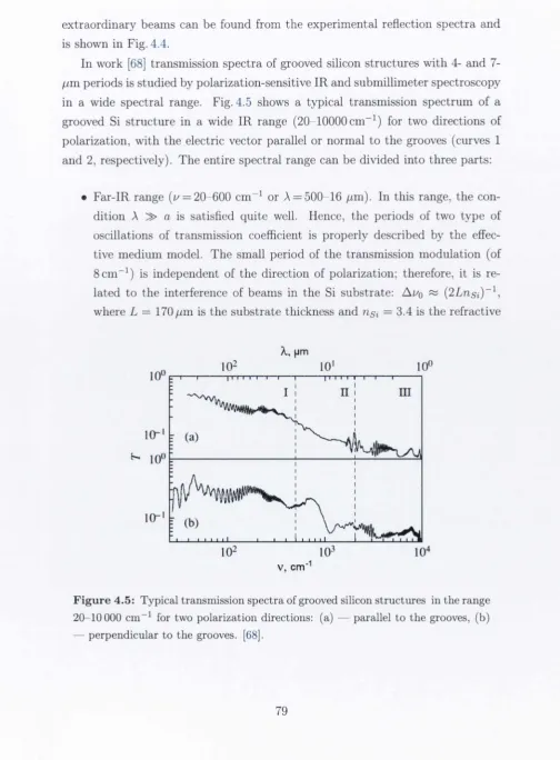
4.5 Typical transmission spectra of grooved silicon structures in the
range 20 10000 cm“^ for two polarization directions: (a) par
allel to the grooves, (b) perpendicular to the grooves. [68].
. .
4.6 Classification of methods of silicon microstructuring...
4.7
4.8
4.9
Schematic of the sample and the optical measurement: silicon sub
strate; iSii (5_
l) section parallel (perpendicular) to the grooves; the
dashed straight line is the normal to the silicon wall;
b
is the width
of the grooves in the bottom part of the structure;
w
and
wqare the
widths of solid silicon stripes between the grooves on the surface
of the sample and the groove depth, respectively. ...
78
79
81
83
85
Schematics of a grooved Si structure for calculations by the scat
tering matrix method: (a) ideal sample model; (b) real sample
model which takes into account the diffuse scattering... 84
Experimental (thick line) reflection spectrum of grooved silicon
sample s6 and reflection spectra calculated for ideal sample model
for the cases of a finite (Fig. 4.8(a), thin gray line) and semi-infinite
(thin black line) silicon substrates for the
E^\
polarization of light.
4.10 Experimental (solid lines) and calculated (dashed lines) reflection
spectra of grooved silicon samples .s5 and s6 for the Ey- and E_i_-
polarizations. Calculations assume the presence of a scattering
layer on the modulated layer-substrate interface for which the com
plex refractive index is set equal to 3.42 -|- 0.5i; the refractive index
of silicon in the modulated layer is set equal to 3.42 -|-
0.2i
and
that of air is 1 -I- 0.05f (see Fig. 4.8b)...
86
4.11 Experimental (top) and calculated (bottom) reflection spectra of
5.1 Oxide thickness along a sample as measured with spectral
ellipsom-etry. The silicon nanocrystals form near the Si02-to-air interface
as indicated schematically (inset, lower right). A representative
nanocrystal PL spectrum shows typical near-infrared emission (in
set, top left). [17]... 92
5.2 Variation of the 750 nm Kohlrausch 1/e decay rate with oxide
thickness under constant, high power pump conditions (symbols).
The periodicity in the data is explained by additional decay pro
portional to the local pump power (solid line). The grey drawn
lines show bounding quantum efficiencies of 40% and 60%. From
[17]... 93
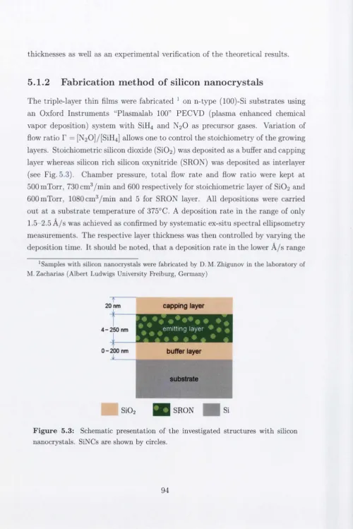
5.3 Schematic presentation of the investigated structures with silicon
nanocrystals. SiNCs are shown by circles... 94
5.4 TEM image of silicon nanocrystals in silicon dioxide matrix [100].
95
5.5 Calculated (lines) and experimental (circles) PL intensities of the
SiNCs samples as a function of the thickness of the buffer layer
(series A) and the thickness of interlayer (series B) for different ex
citation wavelengths... 98
5.6 Comparison of in-coupling (red dashed line) and out-coupling (green
dash-dotted line) efficiencies with calculated (blue solid line) and
experimental (dots) PL intensities of the SiNCs samples as func
tions of buffer layer thickness. Xexc = 325 nm... 99
5.7 In-coupling efficiency (a), out-coupling efficiency (b) and resulted
5.8 PL intensity as a function of interlayer and buffer layer thicknesses
calculated using a model of oscillating dipoles. The white dots
represent experimentally obtained data. The color scale on the
right shows the calculated PL intensity...103
5.9 The highest PL intensity of the samples with silicon nanocrystals
as a function of the total thickness of the sampele... 104
5.10 (a) In-coupling efficiency, (b) out-coupling efficiency and (c) re
sulted PL intensity in the approximation of homogeneous internal
PL spectrum (excitation efficiency)... 106
5.11 (a) Internal PL spectrum, (b) out-coupled PL intensity and (c)
normalized out-coupled PL intensity... 107
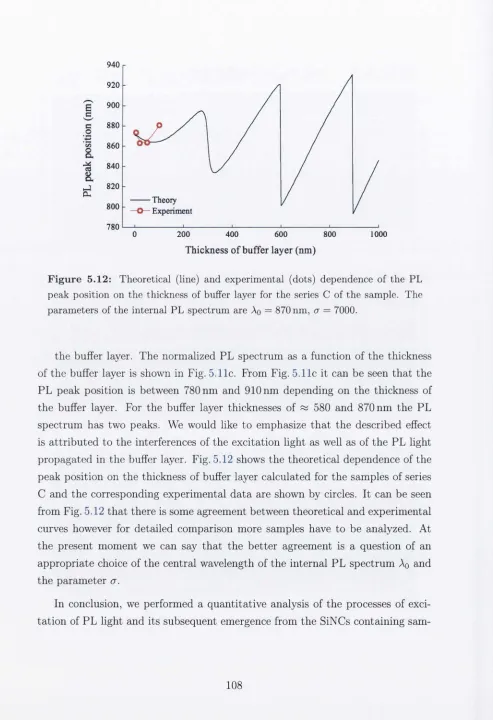
5.12 Theoretical (line) and experimental (dots) dependence of the PL
peak position on the thickness of buffer layer for the series C of
the sample. The parameters of the internal PL spectrum are Aq —
870nm, a = 7000... 108
5.13 Model structure of one-dimensional photonic crystal sample made
of porous silicon. Layers of por-Si, shown by blue and pink col
ors, are considered as homogeneous isotropic layers with refractive
indexes 1.91 and 2.36, respectively. ... Ill
5.14 Reflectance spectra of the investigated multilayered structures mea
sured at normal incidence of light. Vertical dashed and dotted lines
indicate the spectral positions of the employed laser radiation (r'r,),
Stokes
{us),and anti-Stokes
(ua)components of the Raman scat
tering... 113
5.16 Intensity of Stokes component of Raman scattering of the model
structure, shown in Fig. 1 (solid line), and of the homogeneous
layer of por-Si with the thickness of multilayered structure and the
refractive index of 2.36 (dashed line) as a function of the excita
tion wavenumber. The reflection spectrum of the model multilayer
structure is shown by dotted line... 116
5.17 Solid line: calculated average value of square of amplitude of elec
tric filed strength of excitation light (in-coupling efficiency). Dashed
line: calculated Raman intensity for the special case when ampli
tude of the oscillation of electric dipoles does not depend on the
electric field strength of excitation light (out-coupling efficiency).
Dotted line: reflection spectrum from the model multilayer structure. 117
5.18 Raman intensity of the multilayered structures of porous silicon as
a function of the excitation wavenumber and the angle of incidence
of excitation light. Vertical black solid lines denote values of the
parameter Uexc = 2{n\d\ -|- n
2d
2)/\exc which correspond to the
samples NPS-1 and NPS-2. The gray scale on the right shows the
correspondence between the gray shade and the natural logarithm
of Raman intensity... 118
5.19 Schematic of the graphene is an atomic-scale honeycomb lattice
made of carbon atoms...121
5.20 Schematic presentation of the investigated structures with graphene
layer exfoliated onto Si02/Si substrate... 124
5.21 (Color online) Intensity of the G-band of Raman scattering of the
samples with graphene layers as a two-dimensional function of the
a) Si02 and b) AI2O3 buffer layer thicknesses and the excitation
wavelength and as a plot of Iq and hdieiec for c) Si02 and b) AI2O3
at 457 and 633 nm excitations. The selected most common laser
wavelengths corresponding to the extreme values of thicknesses of
both type of buffer layers are shown by red crosses. The buffer
layer thicknesses providing the highest optical contrast for each
5.22 The dependence of the G-band intensity of Raman signal from the
number of graphene layers and the thickness of Si02 and AI2O3
layer calculated for the excitation wavelength of 457 nm...129
5.23 Raman spectra of graphene layers separated from the Si substrate
by different buffer layers. Excitation wavelength is 514 nm... 131
5.24 Raman spectra of graphene exfoliated onto Si02 buffer layer of var
ious thicknesses (90 nm black line, 165 nm red line and 300 nm
— blue line) for different excitation wavelengths: (a) 457 nm and
(b) 633nm... 132
5.25 Calculated (lines) and experimental (symbols) ratios of the inten
sities of Raman 2D-band and G-band as a function of Si02 and
AI2O3 buffer layer thicknesses for different excitation wavelengths. 133
5.26 Calculated (lines) and experimental (symbols) values of the ratio
Ic/lSi
as a function of Si02 buffer layer thickness for different
excitation wavelengths. The experimental data are normalized to
the corresponding theoretical data...134
5.27 Calculated (lines) and experimental (symbols) values of the ratio
Ic/ISi
as a function of AI2O3 buffer layer thickness for different
excitation wavelengths. The experimental data are normalized to
the corresponding theoretical data... 135
5.28 (Color online) Regions of the high Raman intensity (> 0.25/max)
and high total color difference
{AE
>2)... 136
5.29 (Color online) Optical images of the samples with graphene layers
(a), (b) in case of Si02 substrate and (c)-(e) AI2O3 substrate. . . 137
A.l Schematic of the microcavity structure... 160
A. 3 Spatial field distributions of the incident light in the microcav
ity structure, (a), (b), (c): Distributions of the
x-, y-
and z-
components of the electric field along z-direction. (d), (e), (f)
Distributions of the x-,
y-
and z-components of the electric field
along
X-and z-directions. The red (blue) color indicates positive
(negative) values of the electric field strength. The redder (bluer)
means the higher amplitude. A=312nm... 161
B. l Schematic representation of the layered structure with liquid crys
tal. Thick arrows show the orientation of the liquid crystal director,
in the xy-plane in the mirrors and in the cavity. ...165
B.2 Transmission spectra of the silicon one-dimensional photonic crys
List of Tables
4.1 Geometrical parameters of grooved silicon structures... 82
4.2 Effective refractive indexes of grooved silicon calculated from the
Author’s Publications
Peer Reviewed Publications
1. S. A. Dyakov, A. Baldycheva, T. S. Perova, G. V. Li, E. V. Astrova, N. A.
Gippius, and S. G. Tikhodeev, “Surface states in the optical spectra of
two-dimensional photonic crystals with various surface terminations,”
Phys.
Rev. B,
vol. 86, p. 115126, 2012.
2. S. A. Dyakov, D. M. Zhigunov, A. Hartel, M. Zacharias, T. S. Perova,
and V. Y. Timoshenko, “Enhancement of photoluminescence signal from
ultrathin layers with silicon nanocrystals,”
Appl. Phys. Lett.,
vol. 100,
no. 6, p. 061908, 2012.
3. D. M. Zhigunov, S. A. Dyakov, V. Y. Timoshenko, A. N. Yablonskiy,
D. Hiller, and M. Zacharias, “Photoluminescence properties of er-implanted
sio/sio2 multilayered structures with amorphous or crystalline si nanoclus
ters,”
Journal of Nanoelectronics and Optoelectronics,
vol. 6, no. 4, pp. 491-
494, 2011.
4. S. A. Dyakov, E. V. Astrova, T. S. Perova, S. G. Tikhodeev, N. A. Gippius,
and V. Y. Timoshenko, “Optical properties of grooved silicon microstruc
tures: theory and experiment,”
JETP,
vol. 113, no. 1, pp. 80-85, 2011.
5. S. A. Dyakov, E. V. Astrova, T. S. Perova, G. V. Fedulova, A. Baldycheva,
6. I. I. Shaganov, T. S. Perova, V. A. Melnikov, S. A. Dyakov, and K. Berwick,
“Size effect on the infrared spectra of condensed media under conditions of
ID, 2D, and 3D dielectric confinement,” J.
Phys. Chem.
C, vol. 114, no. 39,
pp. 16071-16081, 2010.
7. S. A. Dyakov, D. M. Zhigunov, and V. Y. Timoshenko, “Specific features
of erbium ion photoluminescence in structures with amorphous and crys
talline silicon nanoclusters in silica matrix,”
Semiconductors,
vol. 44, no. 4,
pp. 467 471, 2010.
8. D. M. Zhigunov, V. N. Seminogov, V. Y. Timoshenko, V. I. Sokolov, V. N.
Glebov, A. M. Malyutin, N. E. Maslova, O. A. Shalygina, S. A. Dyakov,
A. S. Akhmanov, V. Y. Panchenko, and P. K. Kashkarov, “Effect of ther
mal annealing on structure and photoluminescence properties of silicon-rich
silicon oxides,”
Physica E,
vol. 41, no. 6, pp. 1006 1009, 2009.
9. S. A. Dyakov, E. V. Astrova, S. G. Tikhodeev, V. Y. Timoshenko, and T. S.
Perova, “Numerical methods for calculation of optical properties of layered
structures,”
SPIE Proc.,
vol. 7521, p. 75210G, 2009.
Selected Talks
1. S. A. Dyakov, D. M. Zhigunov, A. Hartel, M. Zacharias, and T. S. Per
ova, “Interference enhancement of photoluminescence signal from thin lay
ers with silicon nanocrystals,” in
Proceedings of the Microscopical Society
of Ireland Symposium. Program and Abstracts,
(Gork, Ireland), p. 58, Uni
versity College Cork, 29-31 August 2012. Students Best Oral Presentation
Award.
3. S. A. Dyakov, D. M. Zhigunov, T. S. Perova, A. Hartel, D. Hiller, and
M. Zacharias, “Modeling of photoluminescence intensitiy of ultrathin layer
with silicon nanocrystals,” in SPIE Optics + Photonics. Technical Program,
(San Diego, California, USA), p. 61, Convention Center, 23 -27 August 2011.
4. S. A. Dyakov, A. Baldycheva, T. S. Perova, E. V. Astrova, and S. G.
Tikhodeev, “Optical properties of two-dimensional photonic crystal bars
obtained by photoelectrochemical etching of silicon,” in Proceedings of the
Microscopical Society of Ireland and the Northern Ireland Biomedical Engi
neering Society Joint Annual Symposium, (Jordanstown, Northern Ireland,
UK), pp. 11, 18, University of Ulster, 25 27 August 2010.
5. S. A. Dyakov, “Optical characterization of aluminium oxide nanolayers
deposited on si membrane,” in Queens University Belfast joint seminar,
(Belfast, Northern Ireland, UK), Queens University Belfast, 24 August
2010
.6. S. A. Dyakov and D. M. Zhigunov, “Spatial light localization in grooved
silicon matrix,” in Program of X International Conference La,ser and Laser
Information Technologies, (Smolyan, Bulgaria), p. 6, 18 22 October 2009.
Selected Posters
1. S. Dyakov, T. Perova, and Y.-H. Xie, “Interference enhancement of raman
signal from layer of graphene,” in Procedings of the International Conference
on Nanoscience -h Technology, (Paris, Prance), p. 154, Sorbonne, 23 27 July
2012
.3. A. Baldycheva, S. A. Dyakov, Y. A. Zharova, E. V. Astrova, G. Fedulova,
K. Berwick, and T. S. Perova, “Multi-component band-gap devices for inte
grated silicon microphotonics,” in
Conference programme of International
Conference Photonics Ireland,
(Malahide, Ireland), p. 2, 7-9 September
2011
.4. S. A. Dyakov, E. V. Astrova, T. S. Perova, G. V. Fedulova, A. Baldycheva,
T. V. Yu., S. G. Tikhodeev, and N. A. Gippius, “Optical spectra of two-
dimensional photonic crystal bars based on macroporous si,” in
Technical
Summaries of 20th International Congress on Photonics in Europe,
(Mu
nich, Germany), p. 15, International Conference Centre, 23 26 May 2011.
5. S. A. Dyakov, S. G. Tikhodeev, E. V. Astrova, T. S. Perova, and T. V.
Yu., “Investigation of optical properties of one and two-dimensional pho
tonic crystals by means of the scattering matrix method,” in
Technical Pro
gramme of SPIE Photonics Europe,
(Brussels, Belgium), p. 45, The Square
Conference Center, 12 16 April 2010.
6. S. A. Dyakov, E. V. Astrova, T. S. Perova, G. V. Fedulova, A. Baldycheva,
T. V. Yu., S. G. Tikhodeev, and N. A. Gippius, “Optical spectra of two-
dimensional photonic crystal bars based on macroporous si,” in
Technical
Programme of SPIE Photonics West,
(San Francisco, California, USA), The
Moscone Center, 22-27 January 2010.
7. A. Baldycheva, S. A. Dyakov, K. Berwick, and T. S. Perova, “Tuning of
the optical contrast in three-component one-dimensional photonic crystals,”
in
Conference programme of International Conference Photonics Ireland,
(Kinsale, Ireland), 14-16 September 2009.
Chapter 1
Introduction
This thesis is devoted to the investigation of optical properties of nano-and mi-
crostructured silicon materials. These structures attracted a great interest of
researches due to their potential in fabrication of photonic and optoelectronic
devices.
One of the main problems of up-to-date microelectronics is an increase of
the information transmission rate. This problem can be solved by creating of
the integrated circuits, which contain both electronic and optical elements where
the information is transferred by photons. A non-direct band gap as well as an
isotropy of the linear optical properties of the main material of microelectronis,
silicon, imposes a restriction on its use in fabrication of optical elements. The way
out of this situation is a construction of silicon-based nano-and microstructures,
which on the one hand possess a strong anisotropy of the optical properties while
on the other hand could be the basis of light-emitting devices. Thus by setting
a specific geometry of these structures, we can control the light propagation in
them. All of these lead to the need for a detailed study of interaction of light
with silicon nano and microstructures.
Chapter 2
Theoretical methods
The evaluation of propagation of the electromagnetic waves through a structure
can be performed by different calculation methods such as plane wave expan
sion method [1], transfer matrix method [4, 11, 12], scattering matrix method
[8, 9, 13], finite-difference time-domain method [10] etc. In the present work the
2x2 Transfer Matrix Method (TMM) and the Scattering Matrix Method (SMM)
are used. The TMM is applicable for calculation of optical characteristics of mul
tilayered structures whereas the SMM is the most useful method for investigation
of optical properties of structures with complex geometry.
2.1 Transfer matrix method
2.1.1
Calculation of passive optical response
2.1.1.1
Mathematical problem of TMM
Let us consider a system of the
N
parallel layers placed between two semi-infinite
media fioi and
ho
2(Fig. 2.1). All substances are considered to be linear homoge
neous and isotropic. We assume that the wave vector of incident light is
k,
the
polarization of incident light is linear and is characterized by the known direction,
thicknesses of layers
dj {j = 1, 2, ..., N),
their complex dielectric permittivities
ij
=
— e'-i
where
i
is the complex unit and complex magnetic permeabilities
jlj — fi'j — fiji.
We define a z-coordinate of the interface between
j
and j -I- 1
layers as
Zj.
The mathematical problem of the transfer matrix method is the
calculation of the reflection, transmission and absorption coefficients and electro
magnetic field distribution of a plane electromagnetic wave propagating through
the described layered structure.
2.1.1.2 Plane electromagnetic waves in media
In accordance with the approach described in [11], let us consider a linearly polar
ized plane electromagnetic wave traveling at an angle
of if (0 <
< n/2)
to the
positive^ direction of z-axis in a homogeneous isotropic medium (see Fig. 2.2a).
The wave vector has the coordinates
k
=
{kx,ky,kz} =
sin tp, 0, ^ coscp}.
^We assume that an electromagnetic wave propagates in the positive direction of z-axis if the angle between the positive direction of z-axis and the wave vector k is less than 7r/2 and in negative direction if this angle is higher than tt/2. We will characterize the propagation of light by the angle of ip < 7r/2.
In
n
Nn
02 z -.w-i.n
n
n
ni
J!
n2
(a)
V2:
(b)
(c)
Figure 2.2: (a) Plane electromagnetic wave traveling in isotropic homogeneous
medium, (b) Two parallel planes z' and z". (c) Interface between two media with
different dielectric permittivities i\ and
£2where the complex refractive index n = n — in = y/Ip,. Let us expand the
electric field vector of the wave into two components, E±_ and E\\, parallel and
perpendicular to the plane of incidence:
E{x,y,z,t) = E\\{x,y,z,t) + E_i_{x,y, z,t).
Components of the electric field vectors can be written as
E\i {x, y, z, t) = Eop sin 9 ■ e'
-ikzZ—ikxX ^^ 1
Ei_{x, y, z, t) = E
qscos 6 ■ e
—ikzZ—ikxX ^ iut(2.1)
(2.2)
(2.3)
where
9
is the angle between vectors
E
and
E_i_.
The unit vectors
5and p have
the coordinates
p = {cos (p, 0, — sincp} ,
(2.4)
s = {0,1,0}.
(2.5)
The vectors s and p are the directions of oscillation of parallel and perpendicular
wave oscillates along ^-direction then this wave is called s-polarized, along
p-
direction the wave is called p-polarized.
Expressions for the components of electric field (2.2) and (2.3) can be written
in the following form:
E\\{x,y,z,t)
=
E\\{z)p-
—ikxX-\-iujt (2
.6
)E±{x,y,z,t) = Ej_{z)s- e
-ikxX~\-iLjt(2.7)
where
E\\{z), E±{z)
are the amplitudes of the electric field at z-coordinate:
E’li(z) =
Eoe~''^^^ sin6
and
E±{z) =
cos0. The magnetic field vector
can be easily obtained from the known relation between the electric and mag
netic field vectors of in plane electromagnetic wave
H =
u = Re
//||(x, y, 2, t) = -\l~E_i{z)p- e-ikxX-hiojt
u X E
, where
(
2
.8
)H^{x,y,z,t) = +^l
^E\\{z)s-The time average energy densities of electric and magnetic fields are
'^E{x,y,z) = ^(^EE*y
(2.9)
(2.10)
WH{x,y,z) = ^
The time average vector of energy flux density is
(s
Ex H*
(
2
.11
)(
2
.12
)2.1.1.3 Plane electromagnetic waves in layered structure
The penetrated wave is partially reflected on the surface z = di and partially
continues traveling into the sample. The plane wave reflected from the surface
z = di is partially transmitted through the surface z = 0 and partially travels
back. As a result the electromagnetic held in each layer is a sum of forward-
and backward-traveling plane waves. Thus, the parallel and perpendicular com
ponents of the electrical held of the electromagnetic wave in
2coordinate of the
stratifled structure can be represented as;
E\i{x,y,z,t) = E^{x,y,z,t) + E^^ {x,y,z,t),
(2.13)
E±{x,y,z,t) = E'l{x,y,z,t) + Ej_{x,y, z,t),
(2.14)
where ;B||j^(a:, y, z, t) and E|j‘_L(x, y, z, t) denote the forward- and backward-traveling
plane waves. The wave vector of forward-traveling plane wave in j-th layer has
the following coordinates:
j^ii) ^ J 27rn,
27rn^ sinv7j,0,-y-cos(/3j !> =
,
while the wave vector of backward-traveling plane wave is:
The expressions for sin ifj and cos y>j can be found from the Snell’s law:
sm(/7j =
noi sin ip
__ ^
rid
(2.15)
(2.16)
(2.17)
cos
Pj= \ 1 —
Uqi sin p
Hi
(2.18)
If the remaining square root in formula (2.18) is negative then the cosine of the
angle of wave propagation can be found from the following formal expression:
cospj
=—i^
riQi sm p
rii
- 1.(2.19)
As
E.f (x, y, 2,
t) = E±
• e‘“^
E^{x, y, z, t)
= E± cos 0
■
E‘^\
where
p± = {±cosy:)j,0,-sinv?j},
s± =
{0,1,0},
then the electric held vectors at 2-coordinate are
E\\
(x, y, 2,
t) = E+ {z)p+
+ E|, (2)y.
~ikxX+iujt(
2
.20
)(
2
.21
)(
2
.22
)(2.23)
E_i{x,y,z,t) = E+{z)s+ + E_^{z)s.
where
E^{z) = E±
sin^e
-ikzZ(2.24)
(2.25)
£^(2) =
E± cos9e
-ikzZ(2.26)
We can obtain the expressions for the parallel and perpendicular components of
the magnetic held from the equations (2.8) and (2.9):
i^\\{.x,y,zj) =
K- El{z)p+ +E^{z)p
~ikxX-\-iujt(2.27)
H_i_{x,y,z,t) = - \ - E^{z)s+ + E. (z)s_
'' y L II II
• e
-ikxX+iuit
(2.28)
As can be seen from equations (2.20-2.24), the electrical held in each layer is
characterized by the amplitudes of forward- and backward-traveling plane waves
E^{z)
and
E^{z)^
and by the components of the wave vector,
kx k^,
in this layer.
Let us now introduce 2 x 1-column vectors of amplitudes
Ej.(z) =
Eliz)
E-{z)
(2.30)
We will skip symbols ” ||” and ”±” for simplicity later on. Thus, the vectors £(
2)
and
k
characterizes the propagation of plane electromagnetic waves in a layer.
2.1.1.4 Phase shift of amplitude vector
Let us consider two plane electromagnetic waves traveling through medium
i
(Fig. 2.2b) in forward- and backward directions:
E'^(x, y, z, t)
=
E~^{z)ae'
-ikxX(2.31)
E (x,y,z,t) = E (z)ae'
-ikxX ^* ci .
(2.32)
where
a
is either
s
or
p.
It is quite easy to obtain the following relation between
amplitudes
E^{z')
and
E^(z'')
from equations (2.25) and (2.26):
E^{z') =
£±(
2")
Equation (2.33) leads to the relation between vectors E(
2') and E(
2")
'e+{z') / ^ik,{z"-z') Q \ 'e+{z'')
E-{z')_
~
0
e-ik^{z"-z')j
E-{z")
More precisely, equation (2.34) can be written as
E(2') =PE(2"),
where
_ /e^k4z"-z') Q \ “ I 0 e.-ik.{z"-z') ) •
(2.33)
(2.34)
(2.35)
(2.36)
2.1.1.5 Interaction of plane wave with an interface
An electromagnetic field of a plane wave traveling in the positive direction in the
homogeneous isotropic medium is characterized by the vector of amplitudes
E{z) =
E^z)
0
(2.37)
Equation (2.37) implies that there is no backward-traveling plane waves, because
E~{z) =
0. In contrast, if a plane wave propagates in the negative direction, the
vector of amplitudes is
0
Eiz) =
(2.38)
E-{z)\
Les us now consider an interface at z'-coordinate between two media
ii
and
£
2- Let then two above described electromagnetic plane waves travel simultane
ously and their angles of incidence are
(fi
and
(p
2(Fig. 2.2c). It is essential that
nisin(/3i =
n
2sm(fi
2-
hi this case the electromagnetic field is characterized by
vectors
E-{z)
Ea{z) =
{z < z'),
(2.39)
E6(^) =
E^z)
(z > z').
(2.40)
_E-{z)_
We would like to find matrix I which makes relation between vectors E(z' — 0)
and E(z' + 0)
'e+{z'
- 0)' _
(
^11 'e+{z' + 0)E-(z'-O)
\hl
^22J
E-(z' + 0)
or briefly
E(z'-O) =IE(z' + 0).
(2.41)
(2.42)
^Strength of electric and magnetic fields as well as vector £(2) are not defined a.t z = Zk, because some of the components of electric and magnetic fields have discontinuity of the first kind at these z-coordinates. Hence in this work we introduce the following notation: z' ± 0 =
Let us consider the special case when only one plane wave is incident on the
z'-interface. The complex amplitudes of the transmitted and reflected plane waves
in media and ei are given, respectively, by
E+{z' + Q) = tE+{z' -Q),
(2.43)
E-(/-0) =rE+(2'-0),
(2.44)
and
E~{z'
+ 0) = 0, where
r
and
t
are the Fresnel reflection and transmission
coefficients of the z'-interface. Elements
In
and
I12
can be found from equations
(2.41), (2.43) and (2.44):
/ _ 1
r
■'ll — Ti ■'12 —r - <
Elements
/21and
I22
can be found by considering another special case when
backward-traveling plane wave interacts with the Zo-interface. Using symmetry
considerations [11] we find that
/21 -
I22-J
r
_1
and therefore
(2.46)
(2.47)
Formulas (2.37)-(2.47) are valid for both components of electric field vector,
however the Fresnel coefficients for parallel and perpendicular components are
different [11]:
i2hK
-t\\ =
2\/ei62/X2^2
r± =
t± =
fi2K - hK
ij,2K + hK
2fi2k'^
(2.48)
(2.49)
e2fiik'^
-f-£ijl2k”
fj'2k'^
+fiik”
where
k'^
and
k"
are the z-components of wave vectors of forward-traveling waves
in media
£1and £
2-Matrix
I
is called an
interface matrix.
It establishes relation between vectors
of amplitudes E(z' — 0) and E(z' -|- 0) at immediately opposite sides of the
zq-2.1.1.6 Transfer matrix
Let us now consider to the stratified structure shown in Fig. 2.1. It consists of two
semi-infinite media, interfaces and spaces between the interfaces. The incident
electromagnetic wave initiates forward- and backward-traveling plane waves in
each layer. The interface and propagation matrices enable us to relate the vector
of amplitudes
£(20—0) before the structure at
2: = 0 with the vector of amplitudes
at any other ^-coordinate.
A matrix T which establishes relation between vectors of amplitudes E(zo —0)
and E(
2iv + 0) is called a
total transfer matrix
of the structure.
Let us denote the propagation matrix between two interfaces
Zk
and Zj+fc
as ]P(zj,Zj+i). According to the equation (2.36), it is given by the following
expression
^ikzdj Q
Q g ihzdj
(2.50)
where is the z-projection of the forward-traveling plane wave in j-th layer. An
interface matrix of the z^-interface is given by
(2.51)
where
rjand
tjare the Fresnel coefficients for the Zj-interface and can be found
by equations (2.48) and (2.49)L
Therefore, the total transfer matrix for whole structure can be expressed as:
T = I(zo)P(zo,Zi)]I(zi)P(zi,Z
2)I(z
2).. .I(ziv-i)IP(z:w-i,
2iv)I(
2:w)-
(2.52)
2.1.1.7 Reflection, transmission and absorption coefficients
Let us consider an incident forward-traveling plane wave with amplitude
E°{z)
(z < 0). Interaction of this wave with the layered structure leads to appearance
of the reflected and transmitted plane waves with amplitudes
E~{zq—
0) (
z<
zq)
and
E'^{
zn+ 0) (z >
znWe define a
reflection coefficient
as a ratio of the ^-component of Pointing
vector of the reflected wave to that of the incident wave:
or
R = -^.
(2.53)
The
transmission coefficient
is a ratio of the z-component of Pointing vector of
the transmitted wave to that of the incident wave:
51
T =
-ST'
(2.54)
From equations (2.9) (2.12), (2.53), (2.54) we can obtain the reflection and trans
mission coefficients:
R =
\En\^
(2.55)
T =
fioi Re{kflzN + 0))|£'|f(2v + 0)1^-h |E]l(2iv-h 0)1"
M
o2
Re{kflzQ -0))
En
(2.56)
The
absorption coefficient
is defined is a portion of energy of the incident light
which is absorbed by the substances of the layered structure and can be found
from the expression
A = l- R-T.
(2.57)
It is assumed that the amplitude of incidence plane wave at z = lime_>.o(—£■) =
zq
— 0 is known and equals to
E
q,
whereas the amplitudes of reflected and trans
mitted plane waves are unknown. We can use the total transfer matrix and
calculate these amplitudes and, therefore, calculate the reflection, transmission
and absorption coefficients of the given layered structure.
In terms of transfer matrix the interaction of the incidence plane wave with a
layered structure can be written as
Eo
E-{zo -
0
)= T
E+{
zn+ 0)
0
(2.58)
where £o is the amplitude of the incident wave and is equal to 1. Zero compo
nent in the vector of amplitudes in equation (2.58) reflects the fact that there
created by incident wave from the upper semi-infinite medium. Equation (2.58)
leads to the following relation between the amplitudes of incident, reflected and
transmitted waves:
Eq — TiiE'^(zn + 0)
E (
zq~ 0) = T2
iE^{
zn+ 0).
(2.59)
(2.60)
Thus,
1 E''*"(Ziv + 0) =
■' 11
T
E-~{zo-0) =^Eo-J11
(2.61)
(2.62)
Using equations (2.53), (2.61) we obtain the following expression for reflection
coefficient:
T
2111
sim d +
21T-'-
11cos^ 6
(2.63)
where and are elements of the transfer matrix T^l for parallel component
of the fields, while and are for perpendicular component.
Comparison between equations (2.54) and (2.62) leads to expression for trans
mission coefficient:
^ ^ ^ Rejk^jzN +
0
))/202
Re{k^{zo -
0
))1
E
11
sin^ 6 +
11cos^ 6
(2.64)
Thus, the knowledge of the total transfer matrix of the layered structure enables
us to find the reflection, transmission and absorption coefficients.
2.1.1.8 Distribution of the electromagnetic field
Let us consider a linearly polarized plane electromagnetic wave with an amplitude
E
q, a wave vector k and angle of polarization B. This wave is incident on the
electrical and magnetic fields at coordinate
z = h, Zk < h < Zk+i-
The transfer
matrix between coordinates
Zo — 0
and
h
is
Tfc = T(2
o- 0,
h) =
I(2:
o)1P(2
o, 2
i)I(
zi)P(2
i,
22)
1(
22) • • • I(2fc)P(2fc,
h).
(2.65)
According to the definition of the transfer matrix T^,
£0
E~{zo -
0)
= T,
E^ih)
E-{h)
(2
.66
)where
£0=
E^{
zq—
0) is the known amplitude of the incident plane wave. Then
(2.67)
-T
E'^{zi^
+ 0)
0
£0E-(zo-0)_
where T is the total transfer matrix of the structure. Zero component in the
vector of amplitudes in the right side of the equation (2.67) means that there is
no wave incident on the sample from the bottom semi-infinite medium. Equation
(2.67) also means that
and, therefore,
£0 — T\\E^{zn + 0)
E
(20— 0) =
T2iE'^{zf^ +
0),
T
E~{zo
-0
) =-f
11(
2
.68
)(2.69)
(2.70)
From equations (2.66), (2.70) it follows that
’
1
'T21
>(h)'
E-ih)
L'fiJ
(2.71)
and thus.
E*(h)
E-(h)
-1= £oTr • ^
T,
11Tu
T
21(2.72)
Formulas (2.65)-(2.72) are valid for both parallel and perpendicular components
We calculated amplitudes of the electric field at /i-coordinate for forward-
and backward traveling plane waves by means of the transfer matrix. Using
equations (2.23) and (2.24) we can determine the total amplitudes of the parallel
and perpendicular components of the electric field. Then using equations (2.10)
and (2.12) we can obtain the time average electric and magnetic energy densities
and the time average Pointing vector at any (x,
2)-coordinate.
2.1.2 Calculation of active optical response
In addition to calculation of the reflection, transmission and absorption coeffi
cients, the evaluation of other optical characteristics of the stratified structure
such as the intensity of photoluminescence (PL) and Raman scattering is of in
terest too.
Irrespective to the origin of the photoluminescence and the Raman scattering,
the PL or Raman light can be out-coupled from the sample or loosen by different
loss mechanisms [15, 16, 16, 17, 18, 19]. Among the loss mechanisms there are
an absorption by the substrate or other layers, a coupling to the wave-guided
or leaky modes [20, 21, 22], a Rayleigh scattering on the local inhomogenieties
of the spatial distribution of the refractive index [23]. Despite the fact that
the photoluminescence and the Raman scattering are the quantum mechanical
processes, the contribution of all of these mechanisms can be described in terms
of the classical electromagnetism.
In the oscillating dipole approach, the intensity of PL or Raman scattering is
approximated by the intensity of the system of oscillating electrical dipoles placed
in the active layer.
2.1.2.1 System oscillating electrical dipoles
expression:
diy 3.2,
=
71“ sin th
dCl
J 2:
Stt(2.73)
Due to the axial symmetry, the radiation of the vertical dipole is purely p-
polarized. The angular radiation pattern for vertical dipole is shown in Fig. 2.3.
The radiation of the system of horizontal chaotically oriented dipoles has both
s- and p-components. The angular radiation pattern is defined by the following
expressions:
yLY
3
dfl) XY l^TT
COS^Ip
(2.74)
dO.) XY
IGtt(2.75)
Electromagnetic field of an oscillating dipole is a wave with a complex wave
front profile. For the calculation of the intensity of light, emitted by dipoles and
emerged from the sample, one have to approximate the radiation of dipoles by
the plane waves, which amplitude depends on the direction of their propagation.
As follows from the equations (2.75), (2.74) and (2.73), the amplitudes of the
plane waves corresponding for the vertical dipoles are
As = 0,
Ap = Ao\ —sin Ip,
V
OTTand for the horizontal chaotically oriented dipoles
(2.76)
As — Ar
‘s — 77r~i Tip —A
q167r’ IGtt
cos-ip.
(2.77)
The propagation of the plane waves with given amplitudes both inside and outside
the layered structure is fully described by the transfer matrix method.
2.1.2.2 Change of the vector of amplitude at the radiating plane
It can be shown [15] that the boundary conditions for the electric and magnetic
fields in case of the plane of electric currents leads to the following expression for
the change of the vector of amplitudes at the radiating plane at ^'-coordinate
E{z’
- 0) =
E{z'
+ 0) + A,
(2.78)
where for vertical dipoles
A = A.
1
(2.79)
and for horizontal chaotically oriented dipoles
A = As
1
A = A.
(2.80)
Note that the amplitude parameters A^ and Ap are related to each other by equa
tions (2.76) and (2.77). The parameter A
qfrom these equations is proportional
to the absolute value of the amplitude of electric field strength of excitation light
at z'-coordinate:
Ao = a|^exc(0,0,2',0)|.
(2.81)
2.1.2.3 Out-coupling of the emitted light from the sample
In calculating the intensity of out-coupled dipole radiation, we assume that the
only source of the electromagnetic waves in the layered structure is the plane
of oscillating dipoles. Thus, the amplitudes of the plane waves, incident on the
sample from top and bottom semi-infinite media, are zero. Therefore, the vectors
of amplitudes at z = 0 — 0 and
z = h + Q [h = Z
n)
have the following forms:
E(0 - 0)
0
E-(O-O)
E(zw -l- 0) —
E+{h + 0)
0
(2.82)
For calculation the amplitudes of forward- and backward-traveling plane waves
E'^{h +
0) and
E~{0 —
0), emitted by oscillating dipoles and emerged from the
sample, we have to solve the following system of linear algebraic equations:
E(0 - 0) = AE(z' - 0)
E(z' - 0) =
E{z'
+ 0) + A
E(z' + 0) = BE(/i + 0).
(2.83)
In the set of equations (2.83) the first equation is the relation between vectors
of amplitudes at z = 0 — 0 and z = z' — 0. This relation is established by the
use of the transfer matrix A. The second equation describes the change of the
vector of amplitudes at the plane of oscillating dipoles with coordinate z'. The
last equation is the relation between the vectors of amplitudes at z = z' -f 0 and
z = h.
From the set (2.83) it follows that the amplitude of the plane wave emitted
by the z'-plane of oscillating dipoles and out-coupled from the sample towards
the negative z-direction is defined as
E-{0-0) =
(AA)2 - (AA)i
21(2.84)
11
where the symbol
Xij
denotes the
ij-th
element of a matrix
X.
The expression (2.84) determines the amplitude of the out-coupled plane wave
emitted by one plane of oscillating dipoles at the specified angle of observation
ipobs
which is related to the angle of emission in the active layer,
'ip,
by the Snell’s
law:
Note that the angle of emission ip is needed for calculation of the transfer
matrices A and Bh
2.1.2.4 Total intensity of out-coupled light
We define the angular density of intensity of out-coupled light emitted by a
plane(s) of oscillating dipoles as a power of out-coupled light, dP, per unit solid
angle, dO, and unit sample surface da. In calculating the total intensity of out-
coupled light, we have to account for the change in unit solid angle that is due to
refraction of plane waves or its analog for evanescent waves (see Fig. 2.4a). It can
be shown [15], that the defined angular density of intensity Hi from Ath plane
of oscillating dipoles, located in the j-th layer, can be found from the following
expression:
|2 ^01^z,01
n, =
dP
= |£;-(o-o)|^
(2
.86
)dflda ' * ^
’
where and k^j are
2-components of the wave vector of emitted light in the
top semi-infinite medium and in the j-th layer, respectively. The first term in
equation (2.86) is the square of amplitude of electric field of the plane wave
emitted by Ath plane of the oscillating dipoles and out-coupled from the sample.
This can be found from expression (2.84). The second term in equation (2.86) is
the refraction refinement.
Integration of the angular density of intensity of out-coupled light over the
entire range of angles of observation yields the total power emitted by the unit
square surface to the top semi-infinite medium:
f7r/2
U.{ipobs)sinipobsdipobs-
(2.87)
= 27T [
Jo
Integration of the angular density of intensity of out-coupled light over the range
of angles of observation [0;
ipi]gives the power collected by the lens (see Fig. 2.4b).
The maximum angle ipi is determined by the diameter of the lens and the distance
between sample and the lens.
^In general, the direction of observation is characterized by two angles. For the structure under consideration, all layers are assumed to be homogeneous along x- and y-axis. It enables us to characterize the direction of observation only by the angle ipobs between the direction of
(a)
n
d^obs
n
Figure 2.4: (a): Differential solid angle transfer from one layer to another [15].
(b) Collection of the outside power by the lens.
In order to simulate the total power of PL or Raman scattering from one or
several active layers we have to place
M
equidistant planes of oscillating dipoles
to the active layer (s), calculate the amplitudes of the out-coupled waves emitted
by these planes,
E~{Q
— 0)
{i
= 1,2,...,
M)
at all angles of observation in the
desired range, integrate the angular density of intensity, and, finally, sum the
squares of the obtained powers
M
(2.88) i=l
The number of the emitting planes, M, depends on the thickness of active layer,
the refractive index of active layer and the wavelength of dipole emission, A.
The number M must be chosen in such a way that the distance between two
nearest planes
Az
satisfies the following relation:
UkAz
A.
Equation (2.88) describes the outside power emitted by either vertically or